EP0445036B1 - Polykristalliner Silicium-Stab für das Zonenziehen und Verfahren zu seiner Herstellung - Google Patents
Polykristalliner Silicium-Stab für das Zonenziehen und Verfahren zu seiner Herstellung Download PDFInfo
- Publication number
- EP0445036B1 EP0445036B1 EP91400544A EP91400544A EP0445036B1 EP 0445036 B1 EP0445036 B1 EP 0445036B1 EP 91400544 A EP91400544 A EP 91400544A EP 91400544 A EP91400544 A EP 91400544A EP 0445036 B1 EP0445036 B1 EP 0445036B1
- Authority
- EP
- European Patent Office
- Prior art keywords
- silicon rod
- polycrystalline silicon
- monocrystalline
- monocrystalline silicon
- rod
- Prior art date
- Legal status (The legal status is an assumption and is not a legal conclusion. Google has not performed a legal analysis and makes no representation as to the accuracy of the status listed.)
- Expired - Lifetime
Links
- 229910021420 polycrystalline silicon Inorganic materials 0.000 title claims description 64
- 238000000034 method Methods 0.000 title claims description 38
- 229910021421 monocrystalline silicon Inorganic materials 0.000 claims description 63
- XUIMIQQOPSSXEZ-UHFFFAOYSA-N Silicon Chemical group [Si] XUIMIQQOPSSXEZ-UHFFFAOYSA-N 0.000 claims description 31
- 229910052710 silicon Inorganic materials 0.000 claims description 15
- 239000010703 silicon Substances 0.000 claims description 15
- UFHFLCQGNIYNRP-UHFFFAOYSA-N Hydrogen Chemical compound [H][H] UFHFLCQGNIYNRP-UHFFFAOYSA-N 0.000 claims description 11
- 238000010438 heat treatment Methods 0.000 claims description 11
- 238000005530 etching Methods 0.000 claims description 8
- 239000000126 substance Substances 0.000 claims description 6
- 239000007789 gas Substances 0.000 claims description 5
- 239000011247 coating layer Substances 0.000 claims description 4
- 238000000151 deposition Methods 0.000 claims description 4
- 239000004065 semiconductor Substances 0.000 claims description 3
- 239000003039 volatile agent Substances 0.000 claims description 3
- 239000013078 crystal Substances 0.000 description 12
- 239000001257 hydrogen Substances 0.000 description 9
- 229910052739 hydrogen Inorganic materials 0.000 description 9
- 239000011162 core material Substances 0.000 description 6
- 238000002425 crystallisation Methods 0.000 description 6
- 230000008025 crystallization Effects 0.000 description 6
- ZDHXKXAHOVTTAH-UHFFFAOYSA-N trichlorosilane Chemical compound Cl[SiH](Cl)Cl ZDHXKXAHOVTTAH-UHFFFAOYSA-N 0.000 description 6
- 239000005052 trichlorosilane Substances 0.000 description 6
- 238000004857 zone melting Methods 0.000 description 6
- 230000008018 melting Effects 0.000 description 5
- 238000002844 melting Methods 0.000 description 5
- 239000010410 layer Substances 0.000 description 4
- 230000007547 defect Effects 0.000 description 3
- VEXZGXHMUGYJMC-UHFFFAOYSA-N Hydrochloric acid Chemical compound Cl VEXZGXHMUGYJMC-UHFFFAOYSA-N 0.000 description 2
- 238000003486 chemical etching Methods 0.000 description 2
- 229910021419 crystalline silicon Inorganic materials 0.000 description 2
- 230000008021 deposition Effects 0.000 description 2
- 229910000041 hydrogen chloride Inorganic materials 0.000 description 2
- IXCSERBJSXMMFS-UHFFFAOYSA-N hydrogen chloride Substances Cl.Cl IXCSERBJSXMMFS-UHFFFAOYSA-N 0.000 description 2
- 239000000155 melt Substances 0.000 description 2
- 239000002245 particle Substances 0.000 description 2
- 229920001296 polysiloxane Polymers 0.000 description 2
- 230000005855 radiation Effects 0.000 description 2
- VYPSYNLAJGMNEJ-UHFFFAOYSA-N Silicium dioxide Chemical compound O=[Si]=O VYPSYNLAJGMNEJ-UHFFFAOYSA-N 0.000 description 1
- 238000005520 cutting process Methods 0.000 description 1
- 230000001419 dependent effect Effects 0.000 description 1
- 230000000694 effects Effects 0.000 description 1
- 238000010894 electron beam technology Methods 0.000 description 1
- 230000005484 gravity Effects 0.000 description 1
- 239000012535 impurity Substances 0.000 description 1
- 230000006698 induction Effects 0.000 description 1
- 239000011261 inert gas Substances 0.000 description 1
- 230000001788 irregular Effects 0.000 description 1
- 239000000463 material Substances 0.000 description 1
- 239000013081 microcrystal Substances 0.000 description 1
- 239000000203 mixture Substances 0.000 description 1
- 238000002360 preparation method Methods 0.000 description 1
- 239000008213 purified water Substances 0.000 description 1
- 238000000197 pyrolysis Methods 0.000 description 1
- 229910052814 silicon oxide Inorganic materials 0.000 description 1
- 239000011856 silicon-based particle Substances 0.000 description 1
- 239000002344 surface layer Substances 0.000 description 1
- 238000005979 thermal decomposition reaction Methods 0.000 description 1
- XLYOFNOQVPJJNP-UHFFFAOYSA-N water Chemical compound O XLYOFNOQVPJJNP-UHFFFAOYSA-N 0.000 description 1
Images

Classifications
-
- C—CHEMISTRY; METALLURGY
- C30—CRYSTAL GROWTH
- C30B—SINGLE-CRYSTAL GROWTH; UNIDIRECTIONAL SOLIDIFICATION OF EUTECTIC MATERIAL OR UNIDIRECTIONAL DEMIXING OF EUTECTOID MATERIAL; REFINING BY ZONE-MELTING OF MATERIAL; PRODUCTION OF A HOMOGENEOUS POLYCRYSTALLINE MATERIAL WITH DEFINED STRUCTURE; SINGLE CRYSTALS OR HOMOGENEOUS POLYCRYSTALLINE MATERIAL WITH DEFINED STRUCTURE; AFTER-TREATMENT OF SINGLE CRYSTALS OR A HOMOGENEOUS POLYCRYSTALLINE MATERIAL WITH DEFINED STRUCTURE; APPARATUS THEREFOR
- C30B29/00—Single crystals or homogeneous polycrystalline material with defined structure characterised by the material or by their shape
- C30B29/02—Elements
- C30B29/06—Silicon
-
- C—CHEMISTRY; METALLURGY
- C30—CRYSTAL GROWTH
- C30B—SINGLE-CRYSTAL GROWTH; UNIDIRECTIONAL SOLIDIFICATION OF EUTECTIC MATERIAL OR UNIDIRECTIONAL DEMIXING OF EUTECTOID MATERIAL; REFINING BY ZONE-MELTING OF MATERIAL; PRODUCTION OF A HOMOGENEOUS POLYCRYSTALLINE MATERIAL WITH DEFINED STRUCTURE; SINGLE CRYSTALS OR HOMOGENEOUS POLYCRYSTALLINE MATERIAL WITH DEFINED STRUCTURE; AFTER-TREATMENT OF SINGLE CRYSTALS OR A HOMOGENEOUS POLYCRYSTALLINE MATERIAL WITH DEFINED STRUCTURE; APPARATUS THEREFOR
- C30B13/00—Single-crystal growth by zone-melting; Refining by zone-melting
Definitions
- This invention relates to a polycrystalline silicon rod for preparing a monocrystalline silicon rod (or a single crystalline silicon rod) by a floating zone melting method (or a floating zone method) and a process for making the polycrystalline silicon rod, and particularly to the same for preparing the monocrystalline silicon rod for a semiconductor by the single floating zone method and the process for making the same.
- the floating zone method has been developed by paying attention to properties of silicon that its density is relatively low and its surface tension is high, wherein a molten portion of silicon is lain between an unmelted portion of the polycrystalline silicon rod and a solidified portion thereof, a part of the molten portion is kept in a floating state (such molten portion is hereinafter referred to as a floating molten zone) and monocrystalline silicon is grown from a melt which is obtained by melting the polycrystalline silicon rod, without being brought into contact with a container to support the melt and any other materials.
- Japanese Patent Publication No. 56-39048 describes that, with respect to a polycrystalline silicon rod with a seed crystal of monocrystalline silicon being attached to the lower end and which is vertically held, a boundary surface between the seed crystal and the polycrystal line rod is heated and molten by high frequency induction heating, electron beam heating, radiation heating or the like to form the floating molten zone and the thus molten portion is crystallized and the single crystal is grown, while gradually moving the above seed crystal portion downward with rotating and enlarging the size of said floating molten zone.
- the crystallization according to single passage of the floating molten zone does not result in satisfactory monocrystallization, and therefore the monocrystalline silicon rod is prepared through crystallization of the polycrystalline silicon rod in which at least two passages of the floating molten zone are carried out, in said first passage the polycrystalline silicon bar being in part monocrystallized.
- This invention aims at solving the above problem raised in the case that the single crystal is prepared by carrying out twice the passage of the floating molten zone.
- a polycrystalline silicon rod for preparing a monocrystalline silicon rod for a semiconductor by a vertical floating zone method wherein the monocrystalline silicon rod is prepared by a single passage of the floating molten zone through said polycrystalline silicon rod, said polycrystalline silicon rod being characterized in that it comprises:
- the above object is obtained by a method for making a polycrystalline silicon rod according to claim 1, said polycrystalline silicon rod being such that polycrystalline silicon rod is formed around a monocrystalline silicon rod by a chemical vapor growth method to result in the central portion of its section being composed of essentially a monocrystalline silicon structure, said method comprising chemically etching the surface of the monocrystalline silicon rod, heating the monocrystalline silicon rod to a temperature of about 1150°C in a hydrogen gas stream after etching to remove oxide formed on the surface of the monocrystalline silicon rod and thereafter depositing monocrystalline silicon on the polycrystalline silicon rod by the chemical vapor growth method at temperature of about 1100°C and then increasing flow rate of the diluted gas and the concentration of a volatile compound of silicon in gas to form a coating layer of the polycrystalline silicon comprising unit monocrystal grains.
- the monocrystalline silicon structure portion in the polycrystalline silicon rod is comprised of coarsened monocrystal qrains, and said portion is formed over an area around the centre of the radial section the polycrystalline silicon rod, said area being equal to or larger than that of the minimum section of the molten zone during embodiment of the floating zone method.
- a mono-crystalline silicon rod having no defect or less defect can be prepared from the polycrystalline silicon rod of this invention with much higher yield and as well by an single passage of the floating molten zone in the floating zone method. This is extremely economical as compared with the prior art.
- the polycrystalline silicon rod is formed in such a manner that the section of the coarsened region having the coarsened silicon monocrystal grains which is provided with the central portion of the section becomes larger than the minimum section in the molten zone in the zone melting method.
- the size of the section of the coarsened region is determined in such a manner that monocrystalline silicon is easily obtained by a single passage of the floating molten zone.
- the section of the region of the coarsened monocrystal grains in the polycrystalline silicon rod is approximately circular and is 30 mm to 50 mm in diameter, since the monocrystalline silicone is prepared with a high yield.
- the unit monocrystal grain is coasened so that disorder of crystallization does not occur in the monocrystalline silicon rod which is prepared by the floating zone method. Therefore, in order to prepare the polycrystalline silicon rod of this invention, for example, a thin rod of monocrystalline silicon in the form of a square pillar which is cut out from a monocrystalline silicon rod is heated, for example, for 1 to 10 hours in a hydrogen atmosphere and further is subjected to a vapor chemical etching to cleanse the surface thereof and simultaneously to eliminate the surficial crystal defect.
- This heating and vapor etching of the thin rod composed of monocrystalline silicon can be carried out, for example, at a temperature range of 900 to 1200 °C under a hydrogen atmosphere and an atmosphere of hydrogen chloride or the like. It may be satisfactory to carry out the heating only under the hydrogen atmosphere.
- decomposed or reduced silicon atoms are deposited on the surface of the thin rod of monocrystalline silicon under such condition that a monocrystalline layer epitaxially grows thereon at least at an early stage.
- This epitaxial growth can be carried out by the prior method, for example, by way of thermal decomposition or hydrogen reduction of trichlorosilane. Though the qrowth fails in general to go on as it physically means, this epitaxial growth is carried out at 1100 °C. It is preferred to form at least larger crystal grains of crystalline silicon, because it is absolutely need to prepare a monocrystalline silicon rod with higher yields by the zone melting method.
- the region having a satisfactory size wherein it is a polycrystalline structure on the whole but the unit monocrystal grain is coarsened, is formed in the central portion of the section of the polycrystalline silicon rod for preparing the monocrystalline silicon rod by the floating zone method, for example, along an overall length thereof.
- unmelted polycrystal micrograins run down the surface of the molten zone from the polycrystalline portion during embodiment of the zone melting method at the upper part of a portion having the minimum diameter which is in the neighborhood of approximately the center in the longitudinal direction of the molten zone and attain to an exposed end of a solidified portion in the lower part of the molten zone, whereby the crystallization of the solidified portion is effected without being disordered or disarranged.
- the central portion of the polycrystalline silicon rod is composed of micro monocrystal grains
- these micro monocrystal grains are molten
- the melting in the grain boundary therebetween progresses
- the monocrystal grains are isolated in unmelted state, and the isolated grains are exposed on the surface of the molten zone according to difference in the specific gravity and cooled.
- the disordered crystal structure is presented.
- these monocrystal grains are coarsened as in this invention, the monocrystal grains cannot be easily isolated. Therefore, the monocrystallization in this invention becomes remarkably easy, particularly as compared with the case of extremely micro monocrystal grains around the centre of the polycrystalline rod.
- the thin rod of monocrystalline silicon for example, in the form of a square pillar or a column is provided as a core material for preparing the polycrystalline silicon rod and then the surface of the thin rod is heated at a high temperature under hydrogen and hydrogen chloride atmosphere, whereby oxides and other impurities of the surface are volatilized and removed and the resulting surface is free from disorder.
- This thin monocrystalline silicon rod is heated to a temperature of not less than 1000 °C by applying directly an electric current therethrough or an external radiation heating and is brought into contact with a mixture of a volatile compound of silicon such as trichlorosilane and hydrogen to allow silicon atoms to deposit thereon.
- a volatile compound of silicon such as trichlorosilane and hydrogen
- the surface of the thin monocrystal rod has approximately complete monocrystalline structure and thus silicon atoms to be deposited can epitaxially grow. Therefore, these deposited silicon atoms are not only built up as an aggregate of the coarsened monocrystal grains, but often is formed as a large monocrystalline region which is sufficiently recognizable by the naked eye, in the form of a square pillar with each side of about 5 mm.
- the monocrystalline region with a width of 1-4 mm is formed in the four directions ⁇ 110> perpendicular to each other from the side surface of the thin monocrystal rod with the axis derection of ⁇ 100> and toward the outer periphery in straight lines.
- the unit monocrystal grain is coarsened preferably along the overall length at the central portion but it is recommendable that the outer periphery is formed by the polycrystalline layer composed of the minute or fine monocrystal grains.
- the mechanical or thermal properties thereof lose any direction dependent property and, during the progress in the floating zone method, undesirable cracks do not occur in the unmelted portion of the polycrystalline silicon rod and also ununiform melting does not occur.
- this micro unit monocrystal grain in the outer layer causes no problem unlike that in the central portion.
- a monocrystalline silicon rod in the form of a square pillar having one side of the end of about 5 mm and a length of 90 mm (which corresponds to the aforementioned core material) was cut out with selected crystal plane wherein the longitudinal direction is in an axis ⁇ 100> direction and its sides are in a plane ⁇ 100 ⁇ , and an etching was carried out in order to remove fine crystal particles attached when cutting out and residual stress in the surface layer portion.
- the etching allowance was 30 ⁇ m.
- the above square pillar monocrystalline silicon was washed with purified water and dried in an inert gas. The thus dried and cleansed square pillar monocrystalline silicon was heated for 10 hours at 1150 °C under a hydrogen atmosphere. By this heating, oxides which were formed on the surface of the square pillar monocrystalline silicon and the other surface attachments were removed.
- the polycrystalline silicon rod of this example was prepared in such manner as mentioned above, it was possible to prepare monocrystalline silicon with yield of not less than 90 % by a single passage of the floating molten zone in the floating zone method.
- a monocrystalline silicon rod was prepared by using such polycrystalline silicon rod that all the deposition part except the core material portion having the same outer diameter was composed of the fine monocrystal grains and by a single passage of the floating molten zone the yield of the monocrystalline silicone was as low as not more than 10 %.
- the monocrystalline silicon rod in the form of the square pillar was cut out from a larger monocrystalline silicon rod to make the polycrystalline silicon rod for use in the floating zone method.
- a monocrystalline silicon rod may be cut out in the form of a cylindrical column having a diameter of about 5 mm therefrom to make a polycrystalline silicon rod.
- the above column-shaped core material was prepared directly from the polycrystalline rod by melting and solidifying it so as to attain a longitudinal crystal direction of ⁇ 100>.
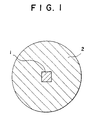
- Fig. 1 shows a schematic sectional view of one embodiment of the polycrystalline silicon rod according to the prior art.
- a central portion (1) of the polycrystalline silicon rod was formed with a thin monocrystalline rod (which corresponds to the core material) in the form of a cylindrical column or square pillar and polycrystals (2) were deposited around the thin rod.
- the polycrystalline silicon rod was formed in such manner that fine monocrystal grains became intricate in the disarranged or irregular direction and were grown as polycrystalline on the whole, and the outer most periphery thereof was in an approximately complete circle.
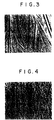
- a monocrystal (3) could be formed in the four radial directions with sizes which was sufficiently observable by the naked eye, as shown in Fig. 2. And, a region (4) surrouded with a line (5) was not clearly observed by the naked eye but it could be confirmed by a microscope that the monocrystalline grains were coarsened. When the microscope magnified this portion about 200 times, it could be observed that the needle-like unit monocrystal grains having a length of 2 to 3 mm were coarsened as shown in Fig. 3.
- the unit monocrystal fine in the outer periphery (the outer layer portion of the line 5) 2 as shown in Fig. 2 was extremely small.
- the microscope magnified the grain portion about 200 times it could be observed that the shape of the grain was not clear and the size thereof was not more than one tenth as long as the unit monocrystal grain in the central polycrystalline portion (Fig. 4).
Landscapes
- Chemical & Material Sciences (AREA)
- Engineering & Computer Science (AREA)
- Crystallography & Structural Chemistry (AREA)
- Materials Engineering (AREA)
- Metallurgy (AREA)
- Organic Chemistry (AREA)
- Crystals, And After-Treatments Of Crystals (AREA)
- Silicon Compounds (AREA)
Claims (5)
- Polykristalliner Siliziumstab zur Herstellung eines monokristallinen Siliziumstabes für einen Halbleiter mittels eines vertikalen Schwebezonenverfahrens, wobei der monokristalline Siliziumstab mittels eines einzigen Durchlaufs der Schwebeschmelzzone durch den polykristallinen Siliziumstab hindurch hergestellt wird,
dadurch gekennzeichnet, daß
der polykristalline Siliziumstab folgende Merkmale aufweist:(a) einen Kernbereich (1) aus monokristallinem Silizium mit einer in die <100>-Richtung weisenden Längsachse im Mittelpunkt des Radialquerschnitts des polykristallinen Siliziumstabes und einem mittels eines chemischen Dampfphasenwachstumsverfahrens um den Kernbereich (1) herum epitaktisch aufgewachsenen Bereich (3) aus monokristallinem Silizium und(b) einen ersten Bereich (4) der Querschnittsfläche des polykristallinen Siziliumbereichs, der aus vergröberten monokristallinen Siliziumkörnern gebildet ist und die monokristallinen Bereiche (1, 3) umgibt, und einen zweiten Bereich (2) der Querschnittsfläche, der von feinen mikro-monokristallinen Siliziumkörnern gebildet ist und den ersten Bereich (4) umgibt, wobei der erste Bereich (4) eine Querschnittsflächengröße größer als die minimale Querschnittsflächengröße der Schwebeschmelzzone besitzt und der erste Bereich (4) der Querschnittsfläche aus Aggregaten vergröberter, nadelförmiger monokristalliner Siliziumkörner mit einer Länge zwischen 2mm und 3mm besteht. - Polykristalliner Siliziumstab nach Anspruch 1, wobei der Kernbereich (1) aus monokristallinem Silizium der Mitte des polykristallienen Siliziumstabes eine Dicke von ungefähr 5mm besitzt.
- Polykristalliner Siliziumstab nach Anspruch 2, wobei der erste Bereich (4) der Querschnittsfläche einen Außendurchmesser von ungefähr 30mm bis ungefähr 50mm aufweist.
- Polykristalliner Siliziumstab nach Anspruch 1, wobei der rohe Kernbereich (1) aus monokristallinem Silizium die Gestalt einer rechteckigen Säule besitzt, deren vier Seiten alle in {110}-Ebenen liegen.
- Verfahren zur Herstellung eines polykristallinen Siliziumstabes nach Anspruch 1, wobei der polykristalline Siliziumstab ein solcher ist, der unter Verwendung eines chemischen Gasphasenwachstumsverfahrens um einen monokristallinen Siliziumkern herum gebildet ist, so daß er als Resultat in einem mittigen Bereich seines Querschnitts im wesentlichen aus einer monokristallinen Siliziumstruktur besteht, wobei das Verfahren ein chemisches Ätzen der Oberfläche des monokristallinen Siliziumkerns, ein Erwärmen des monokristallinen Siliziumstabes nach dem Ätzen auf eine Temperatur von ungefähr 1150°C in einem Wasserstoffgasstrom zur Entfernung von an der Oberfläche des monokristallinen Siliziumkerns gebildetem Cxid und danach ein Aufbringen von monokristallinem Silizium auf den monokristallinen Siliziumstab durch das chemische Gasenphasenwachstumsverfahren bei einer Temperatur von etwa 1100°C, um vergröberte monokristalline Körner zu erhalten, und dann ein Erhöhen der Flußrate des verdünnten Gases und der Konzentration einer flüchtigen Siliziumverbindung im Gas beinhaltet, um eine Überzugsschicht aus dem polykristallinen Silizium zu bilden, das mikro-monokristalline Einheitskörner enthält.
Applications Claiming Priority (2)
| Application Number | Priority Date | Filing Date | Title |
|---|---|---|---|
| JP48954/90 | 1990-02-28 | ||
| JP2048954A JP2516823B2 (ja) | 1990-02-28 | 1990-02-28 | 浮遊帯域融解法による単結晶シリコン製造用の棒状多結晶シリコン及びその製造方法 |
Publications (2)
| Publication Number | Publication Date |
|---|---|
| EP0445036A1 EP0445036A1 (de) | 1991-09-04 |
| EP0445036B1 true EP0445036B1 (de) | 1998-07-08 |
Family
ID=12817671
Family Applications (1)
| Application Number | Title | Priority Date | Filing Date |
|---|---|---|---|
| EP91400544A Expired - Lifetime EP0445036B1 (de) | 1990-02-28 | 1991-02-28 | Polykristalliner Silicium-Stab für das Zonenziehen und Verfahren zu seiner Herstellung |
Country Status (4)
| Country | Link |
|---|---|
| US (1) | US5310531A (de) |
| EP (1) | EP0445036B1 (de) |
| JP (1) | JP2516823B2 (de) |
| DE (1) | DE69129709T2 (de) |
Cited By (1)
| Publication number | Priority date | Publication date | Assignee | Title |
|---|---|---|---|---|
| US7939173B2 (en) | 2007-05-16 | 2011-05-10 | Wacker Chemie Ag | Polycrystalline silicon rod for zone reflecting and a process for the production thereof |
Families Citing this family (17)
| Publication number | Priority date | Publication date | Assignee | Title |
|---|---|---|---|---|
| JP2874722B2 (ja) * | 1993-06-18 | 1999-03-24 | 信越半導体株式会社 | シリコン単結晶の成長方法及び装置 |
| JP3357675B2 (ja) * | 1996-05-21 | 2002-12-16 | 株式会社 トクヤマ | 多結晶シリコンロッドおよびその製造方法 |
| KR100499958B1 (ko) * | 1999-01-22 | 2005-07-11 | 에스케이씨 주식회사 | 이미지 수용층용 조성물 및 이로부터 형성된 이미지수용층을 구비한 고분자 필름 |
| US6623801B2 (en) * | 2001-07-30 | 2003-09-23 | Komatsu Ltd. | Method of producing high-purity polycrystalline silicon |
| EP2021279A2 (de) * | 2006-04-13 | 2009-02-11 | Cabot Corporation | Verfahren zur herstellung von silicium durch ein verfahren mit geschlossenem kreislauf |
| JP5137670B2 (ja) * | 2008-04-23 | 2013-02-06 | 信越化学工業株式会社 | 多結晶シリコンロッドの製造方法 |
| CN101717990A (zh) * | 2008-10-10 | 2010-06-02 | 江西赛维Ldk太阳能高科技有限公司 | 高纯多晶硅棒作为供料棒在单晶硅区域熔炼法中的应用以及制备方法 |
| MY153052A (en) * | 2009-02-04 | 2014-12-31 | Tokuyama Corp | Process for producing polycrystalline silicon |
| CN102471868B (zh) * | 2009-07-02 | 2014-08-27 | 松下电器产业株式会社 | 薄膜制造方法及能够用于其方法的硅材料 |
| KR101382657B1 (ko) * | 2009-11-06 | 2014-04-07 | 제이엑스 닛코 닛세키 킨조쿠 가부시키가이샤 | 하이브리드 실리콘 웨이퍼 |
| JP5309224B2 (ja) * | 2009-11-06 | 2013-10-09 | Jx日鉱日石金属株式会社 | ハイブリッドシリコンウエハ |
| CN103160912B (zh) * | 2011-12-08 | 2015-11-11 | 有研半导体材料有限公司 | 一种掺杂区熔单晶的制备工艺 |
| DE102011089449A1 (de) * | 2011-12-21 | 2013-06-27 | Wacker Chemie Ag | Polykristalliner Siliciumstab und Verfahren zur Herstellung von Polysilicium |
| JP6135666B2 (ja) * | 2012-05-31 | 2017-05-31 | 富士電機株式会社 | 半導体装置の製造方法 |
| CN103510156A (zh) * | 2012-06-29 | 2014-01-15 | 三菱综合材料株式会社 | 多晶硅棒 |
| JP7128124B2 (ja) | 2019-01-18 | 2022-08-30 | 信越化学工業株式会社 | 多結晶シリコン棒、多結晶シリコンロッドおよびその製造方法 |
| JP7718999B2 (ja) | 2022-01-25 | 2025-08-05 | 信越化学工業株式会社 | 品質評価方法、評価用シリコンの製造システム及び評価用シリコンの製造方法 |
Citations (1)
| Publication number | Priority date | Publication date | Assignee | Title |
|---|---|---|---|---|
| DE2727305A1 (de) * | 1977-06-16 | 1979-01-04 | Siemens Ag | Verfahren zum abscheiden von feinkristallinem silicium aus der gasphase an der oberflaeche eines erhitzten traegerkoerpers |
Family Cites Families (8)
| Publication number | Priority date | Publication date | Assignee | Title |
|---|---|---|---|---|
| US3773499A (en) * | 1968-04-03 | 1973-11-20 | M Melnikov | Method of zonal melting of materials |
| US4196041A (en) * | 1976-02-09 | 1980-04-01 | Motorola, Inc. | Self-seeding conversion of polycrystalline silicon sheets to macrocrystalline by zone melting |
| DE2925679A1 (de) * | 1979-06-26 | 1981-01-22 | Heliotronic Gmbh | Verfahren zur herstellung von siliciumstaeben |
| DE3333960A1 (de) * | 1983-09-20 | 1985-04-04 | Wacker-Chemitronic Gesellschaft für Elektronik-Grundstoffe mbH, 8263 Burghausen | Verfahren zur herstellung von versetzungsfreien einkristallstaeben aus silicium |
| JPS6230698A (ja) * | 1985-07-31 | 1987-02-09 | Fujitsu Ltd | 単結晶成長法 |
| JPH07104578B2 (ja) * | 1987-06-30 | 1995-11-13 | 富士写真フイルム株式会社 | 画像形成方法 |
| DE3804083A1 (de) * | 1988-02-10 | 1989-08-24 | Dow Corning | Verfahren zur herstellung eines polykristallinen halbleitermaterials, polykristalliner stab und einkristall aus einem solchen material |
| US4921026A (en) * | 1988-06-01 | 1990-05-01 | Union Carbide Chemicals And Plastics Company Inc. | Polycrystalline silicon capable of yielding long lifetime single crystalline silicon |
-
1990
- 1990-02-28 JP JP2048954A patent/JP2516823B2/ja not_active Expired - Lifetime
-
1991
- 1991-02-28 DE DE69129709T patent/DE69129709T2/de not_active Expired - Fee Related
- 1991-02-28 EP EP91400544A patent/EP0445036B1/de not_active Expired - Lifetime
-
1992
- 1992-11-30 US US07/983,784 patent/US5310531A/en not_active Expired - Fee Related
Patent Citations (1)
| Publication number | Priority date | Publication date | Assignee | Title |
|---|---|---|---|---|
| DE2727305A1 (de) * | 1977-06-16 | 1979-01-04 | Siemens Ag | Verfahren zum abscheiden von feinkristallinem silicium aus der gasphase an der oberflaeche eines erhitzten traegerkoerpers |
Cited By (1)
| Publication number | Priority date | Publication date | Assignee | Title |
|---|---|---|---|---|
| US7939173B2 (en) | 2007-05-16 | 2011-05-10 | Wacker Chemie Ag | Polycrystalline silicon rod for zone reflecting and a process for the production thereof |
Also Published As
| Publication number | Publication date |
|---|---|
| JP2516823B2 (ja) | 1996-07-24 |
| EP0445036A1 (de) | 1991-09-04 |
| US5310531A (en) | 1994-05-10 |
| JPH03252397A (ja) | 1991-11-11 |
| DE69129709T2 (de) | 1999-02-18 |
| DE69129709D1 (de) | 1998-08-13 |
Similar Documents
| Publication | Publication Date | Title |
|---|---|---|
| EP0445036B1 (de) | Polykristalliner Silicium-Stab für das Zonenziehen und Verfahren zu seiner Herstellung | |
| US7939173B2 (en) | Polycrystalline silicon rod for zone reflecting and a process for the production thereof | |
| JP4147599B2 (ja) | シリコン単結晶及びその製造方法 | |
| KR100994320B1 (ko) | 단결정 실리콘의 제조 방법, 단결정 실리콘 웨이퍼의 제조방법, 단결정 실리콘 제조용 종결정, 단결정 실리콘 잉곳및 단결정 실리콘 웨이퍼 | |
| US4944925A (en) | Apparatus for producing single crystals | |
| JP2833478B2 (ja) | シリコン単結晶成長方法 | |
| JP2022159501A (ja) | 多結晶シリコン棒、多結晶シリコンロッドおよびその製造方法 | |
| JP4060106B2 (ja) | 一方向凝固シリコンインゴット及びこの製造方法並びにシリコン板及び太陽電池用基板及びスパッタリング用ターゲット素材 | |
| US20020020339A1 (en) | Process for preparing a silicon melt | |
| JP4407188B2 (ja) | シリコンウェーハの製造方法およびシリコンウェーハ | |
| US5089082A (en) | Process and apparatus for producing silicon ingots having high oxygen content by crucible-free zone pulling, silicon ingots obtainable thereby and silicon wafers produced therefrom | |
| JPH09235186A (ja) | 単結晶引き上げ用種結晶及び該種結晶を用いた単結晶の引き上げ方法 | |
| JP3069656B1 (ja) | 球状の金属チタン及びチタン化合物の製造方法 | |
| JPH089520B2 (ja) | 薄膜単結晶の製造方法 | |
| JP2574618B2 (ja) | 結晶成長方法と結晶成長用るつぼ | |
| JP2734820B2 (ja) | 化合物半導体単結晶の製造方法 | |
| US5968260A (en) | Method for fabricating a single-crystal semiconductor | |
| JPH07330482A (ja) | 単結晶成長方法及び単結晶成長装置 | |
| JPS61242983A (ja) | 半導体単結晶棒の製造方法 | |
| KR920007340B1 (ko) | Ⅲ-ⅴ화합물 반도체 단결정의 제조방법 | |
| JP2783624B2 (ja) | 単結晶の製造方法 | |
| JPS5950628B2 (ja) | 単結晶シリコン引上げ用窒化珪素製治具 | |
| CS264935B1 (cs) | Způsob úpravy růstových podmínek a pěstování safíru modifikovanou Kyropoulovou metodou | |
| JP3986108B2 (ja) | 石英ガラスルツボ及びその製造方法 | |
| JPH07277891A (ja) | 結晶成長方法 |
Legal Events
| Date | Code | Title | Description |
|---|---|---|---|
| PUAI | Public reference made under article 153(3) epc to a published international application that has entered the european phase |
Free format text: ORIGINAL CODE: 0009012 |
|
| AK | Designated contracting states |
Kind code of ref document: A1 Designated state(s): DE FR GB |
|
| 17P | Request for examination filed |
Effective date: 19920810 |
|
| 17Q | First examination report despatched |
Effective date: 19950807 |
|
| GRAG | Despatch of communication of intention to grant |
Free format text: ORIGINAL CODE: EPIDOS AGRA |
|
| GRAG | Despatch of communication of intention to grant |
Free format text: ORIGINAL CODE: EPIDOS AGRA |
|
| GRAH | Despatch of communication of intention to grant a patent |
Free format text: ORIGINAL CODE: EPIDOS IGRA |
|
| GRAH | Despatch of communication of intention to grant a patent |
Free format text: ORIGINAL CODE: EPIDOS IGRA |
|
| GRAA | (expected) grant |
Free format text: ORIGINAL CODE: 0009210 |
|
| AK | Designated contracting states |
Kind code of ref document: B1 Designated state(s): DE FR GB |
|
| REF | Corresponds to: |
Ref document number: 69129709 Country of ref document: DE Date of ref document: 19980813 |
|
| ET | Fr: translation filed | ||
| PGFP | Annual fee paid to national office [announced via postgrant information from national office to epo] |
Ref country code: FR Payment date: 19990209 Year of fee payment: 9 |
|
| PGFP | Annual fee paid to national office [announced via postgrant information from national office to epo] |
Ref country code: GB Payment date: 19990304 Year of fee payment: 9 |
|
| PGFP | Annual fee paid to national office [announced via postgrant information from national office to epo] |
Ref country code: DE Payment date: 19990305 Year of fee payment: 9 |
|
| PLBE | No opposition filed within time limit |
Free format text: ORIGINAL CODE: 0009261 |
|
| STAA | Information on the status of an ep patent application or granted ep patent |
Free format text: STATUS: NO OPPOSITION FILED WITHIN TIME LIMIT |
|
| 26N | No opposition filed | ||
| PG25 | Lapsed in a contracting state [announced via postgrant information from national office to epo] |
Ref country code: GB Free format text: LAPSE BECAUSE OF NON-PAYMENT OF DUE FEES Effective date: 20000228 |
|
| GBPC | Gb: european patent ceased through non-payment of renewal fee |
Effective date: 20000228 |
|
| PG25 | Lapsed in a contracting state [announced via postgrant information from national office to epo] |
Ref country code: FR Free format text: LAPSE BECAUSE OF NON-PAYMENT OF DUE FEES Effective date: 20001031 |
|
| PG25 | Lapsed in a contracting state [announced via postgrant information from national office to epo] |
Ref country code: DE Free format text: LAPSE BECAUSE OF NON-PAYMENT OF DUE FEES Effective date: 20001201 |
|
| REG | Reference to a national code |
Ref country code: FR Ref legal event code: ST |