EP0445336A1 - Méthode et dispositif de réduction du scintillement du bord d'une image de télévision - Google Patents
Méthode et dispositif de réduction du scintillement du bord d'une image de télévision Download PDFInfo
- Publication number
- EP0445336A1 EP0445336A1 EP90104483A EP90104483A EP0445336A1 EP 0445336 A1 EP0445336 A1 EP 0445336A1 EP 90104483 A EP90104483 A EP 90104483A EP 90104483 A EP90104483 A EP 90104483A EP 0445336 A1 EP0445336 A1 EP 0445336A1
- Authority
- EP
- European Patent Office
- Prior art keywords
- field
- signal
- line
- correction
- fields
- Prior art date
- Legal status (The legal status is an assumption and is not a legal conclusion. Google has not performed a legal analysis and makes no representation as to the accuracy of the status listed.)
- Granted
Links
- 238000000034 method Methods 0.000 title claims abstract description 53
- 238000012937 correction Methods 0.000 claims abstract description 88
- 230000001133 acceleration Effects 0.000 claims abstract description 18
- 230000003111 delayed effect Effects 0.000 claims description 14
- 238000001514 detection method Methods 0.000 claims description 7
- 238000011156 evaluation Methods 0.000 claims description 7
- 230000006870 function Effects 0.000 claims description 3
- 238000005070 sampling Methods 0.000 claims 1
- 230000007704 transition Effects 0.000 description 10
- 230000033001 locomotion Effects 0.000 description 8
- 230000008569 process Effects 0.000 description 6
- 238000012545 processing Methods 0.000 description 5
- 230000001771 impaired effect Effects 0.000 description 3
- 230000009467 reduction Effects 0.000 description 3
- 230000008901 benefit Effects 0.000 description 2
- 230000000694 effects Effects 0.000 description 2
- 230000002123 temporal effect Effects 0.000 description 2
- 108010076504 Protein Sorting Signals Proteins 0.000 description 1
- 230000009471 action Effects 0.000 description 1
- 230000006978 adaptation Effects 0.000 description 1
- 230000003044 adaptive effect Effects 0.000 description 1
- 230000008859 change Effects 0.000 description 1
- 230000000052 comparative effect Effects 0.000 description 1
- 230000000295 complement effect Effects 0.000 description 1
- 238000000354 decomposition reaction Methods 0.000 description 1
- 230000001419 dependent effect Effects 0.000 description 1
- 238000013461 design Methods 0.000 description 1
- 230000006866 deterioration Effects 0.000 description 1
- 238000011161 development Methods 0.000 description 1
- 230000018109 developmental process Effects 0.000 description 1
- 238000010586 diagram Methods 0.000 description 1
- 230000006872 improvement Effects 0.000 description 1
- 230000010354 integration Effects 0.000 description 1
- 238000004519 manufacturing process Methods 0.000 description 1
- 230000002441 reversible effect Effects 0.000 description 1
Images




Classifications
-
- H—ELECTRICITY
- H04—ELECTRIC COMMUNICATION TECHNIQUE
- H04N—PICTORIAL COMMUNICATION, e.g. TELEVISION
- H04N5/00—Details of television systems
- H04N5/14—Picture signal circuitry for video frequency region
- H04N5/21—Circuitry for suppressing or minimising disturbance, e.g. moiré or halo
-
- H—ELECTRICITY
- H04—ELECTRIC COMMUNICATION TECHNIQUE
- H04N—PICTORIAL COMMUNICATION, e.g. TELEVISION
- H04N7/00—Television systems
- H04N7/01—Conversion of standards, e.g. involving analogue television standards or digital television standards processed at pixel level
- H04N7/0127—Conversion of standards, e.g. involving analogue television standards or digital television standards processed at pixel level by changing the field or frame frequency of the incoming video signal, e.g. frame rate converter
- H04N7/0132—Conversion of standards, e.g. involving analogue television standards or digital television standards processed at pixel level by changing the field or frame frequency of the incoming video signal, e.g. frame rate converter the field or frame frequency of the incoming video signal being multiplied by a positive integer, e.g. for flicker reduction
-
- Y—GENERAL TAGGING OF NEW TECHNOLOGICAL DEVELOPMENTS; GENERAL TAGGING OF CROSS-SECTIONAL TECHNOLOGIES SPANNING OVER SEVERAL SECTIONS OF THE IPC; TECHNICAL SUBJECTS COVERED BY FORMER USPC CROSS-REFERENCE ART COLLECTIONS [XRACs] AND DIGESTS
- Y10—TECHNICAL SUBJECTS COVERED BY FORMER USPC
- Y10S—TECHNICAL SUBJECTS COVERED BY FORMER USPC CROSS-REFERENCE ART COLLECTIONS [XRACs] AND DIGESTS
- Y10S348/00—Television
- Y10S348/91—Flicker reduction
Definitions
- the invention relates to a method for reducing the edge flicker of a television picture, in which a first field containing all odd-numbered lines of a frame and a second field containing all even-numbered lines of a frame with a raster frequency that is twice as high as the vertical frequency of the individual fields in a vertical-temporal Scanning grid of the field sequence primary first field, secondary first field, secondary second field and primary second field are displayed on a screen of the television receiver, and an apparatus for performing the method.
- the reproduction of the individual fields provided with the known method with a raster frequency of 100 Hz leads to the fact that the large-area flicker is reduced.
- the increase in the raster frequency from 50 Hz to 100 Hz provided in the known method does not, however, eliminate or reduce the edge flickering that occurs unchanged - as in the standard reproduction of a television picture according to the CCIR standard - with a flickering frequency of 25 Hz that is very irritating to the human eye .
- this known method has the disadvantage that such a repetition of the two fields of a frame leads to an incorrect assignment of the movement phases, as a result of which movement disturbances occur which drastically impair the resolution of the television picture.
- the known method works reasonably satisfactorily only when displaying still images, in particular when displaying characters. However, it is not suitable for displaying moving details in current television pictures.
- a motion-adaptive method is also known (cf. "C.Hentschel: Flicker reduction method for Improvement of television picture reproduction ", ntz-Archiv 7, (1985), pp. 219-229), in which a first and a second field of a frame are temporarily stored in a memory of the television receiver.
- a motion detector is provided which either or Interpolation coefficients are calculated from the temporal and / or vertical change in the image signals occurring in the assigned partial areas, by means of which a weighted superposition of lines of the first and second fields assigned to one another takes place
- This method has the disadvantage that the vertical resolution of the television picture is reduced due to the weighted mixing of corresponding lines of the first and second fields.
- the object is achieved in that for the detection of the edge flicker the luminance signal of one line of a field is compared with the luminance signal of the vertically following line of the temporally following field, and that correction values are derived from the luminance signals of these corresponding lines of the two temporally successive fields, and that a signal-adaptive delay or a signal-adaptive acceleration of corresponding lines of a field is carried out to correct the edge flickering.
- the measures according to the invention have the advantage that the line-by-line comparison of two vertically successive lines of two used for the detection of edge flickering Time-sequential fields are particularly easy to determine, with high resolution, horizontally oriented transitions with high image contrast. In addition, no complicated and complex motion detector is required to detect the luminance differences associated sub-areas of two successive fields.
- the correction of the edge flickering according to the invention by means of the signal-adaptive delay or signal-adaptive acceleration of corresponding lines (or their content) within only a single field means that no motion blur can occur.
- the vertical resolution of the television picture is not impaired by the corrective measures.
- FIGS. 1a to 1f show the reproduction on the receiver side of a frame consisting of a first field A and a second field B, the field sequence A, A ', B', B being selected to reduce the flicker interference.
- FIGS. 1a and 1b show the known intermediate image method (interlace or interlace method) for reducing flicker.
- FIGS. 1c to 1f illustrate the method according to the invention which is improved in comparison.
- the lines 1, 3, ..., 101, 103, 105, ..., 625 defining a first line grid are shown and in the second field B the lines 2, 4, 6, ..., 102, 104, 106, ..., 624 of the full screen contained in the second line grid are transmitted.
- Lines 101 to 107 are shown in the vertical direction and the chronological sequence of the individual fields A and B is shown in the horizontal direction.
- the vertical-temporal scanning grid shown in these figures results from the known AA'B'B cycle of the intermediate image method.
- the first field A which is temporarily stored in a video memory of the television receiver, is first written in the so-called "double-scan mode" as the primary first field A in the first line grid. This is followed by the reproduction of the first field as a secondary field A 'in the second line grid of the field B.
- the second field B following the first field A of a frame is first as a secondary second field B' in the first line grid of the field A and then as the primary second Field B written in the second line grid.
- the reproduction of each primary or secondary field takes 10 ms - corresponding to the raster frequency of 100 Hz.
- a complete field sequence for the reproduction of a frame therefore takes up a period of 40 ms.
- two different constellations are possible, such as a jump in the luminance signal between two lines that follow one another vertically and temporally (i.e. in one field) and thus a contrast difference at horizontally oriented transitions of the television picture that leads to edge flickering can occur.
- the contrast jump can occur first in field A or first in field B.
- the first alternative is that the amplitude of the luminance signal increases from one line of the second field B (here: line 102) to the vertically following line of the temporally following first field A (here: line 103) (signal jump first in the first field A; see FIG. 1a for this , 1c and 1e).
- the amplitude of the luminance signal increases from one line of the first field A (here: line 103) to the vertically following line of the second field B (here: line 104) (signal jump first in the second field B ; see Fig. 1b, 1d and 1f).
- Fig. 1a (signal jump first in the first field A) and in Fig. 1b (signal jump first in the second field B), the frequency and the amplitude of the edge flicker can be seen, as is the case with the above-mentioned, belonging to the prior art Procedure results.
- the period of the edge flickering is 40 ms, i.e. the time span of a complete field sequence A, A ', B', B of a frame.
- the amplitude of the edge flickering and the associated line wandering amount to two lines, whereby the vertical resolution of the television picture is impaired.
- the line 20 shows the vertical-temporal course of the edge flickering, as it results from the application of the method according to the invention described below. It can be seen that the frequency of the edge flickering has increased by a factor of 2 compared to the prior art to a frequency value of 50 Hz. The amplitude of the edge flickering is now one line. However, due to the geometrical-temporal integration effect of the human eye, such a slight image disturbance lies below the viewer's reception threshold!
- the inventive concept of the method is as follows: by comparing the luminance signal of one line of the first field A or the second field B (here: lines 103 or 104) with the corresponding vertically following line of the second field B or the first one preceding the time Field A (here: lines 102 and 103) is determined in which field A or B the above-mentioned signal jump occurs first.
- a difference signal is formed from the luminance signals of the compared lines, the magnitude and phase of which is directly proportional to the step amplitude. From the phase of the jump amplitude it can be immediately determined whether the signal jump in the first field A (cf. Fig. 1a) or in the second field B (see Fig. 1b) takes place.
- the magnitude of the jump amplitude represents a measure of the image contrast difference between adjacent lines.
- This comparison is carried out for all lines of two fields which are consecutive in time.
- the difference signals obtained from this are converted into corresponding correction values, which are stored in a suitable form.
- phase is particularly important when the contrast transition extends over several characters and thus there is a continuous transition instead of a jump (as in FIGS. 1). Specifying the phase can indicate that the transition (50% limit) is between two lines.
- the essential step of the method is that in the event of a signal jump in field A (B), the primary first (second) field A (B) is written on the screen with a delay of up to one line in the vertical direction (FIGS. 1c and 1d ) or the temporally subsequent secondary field B '(A') to "accelerate" up to one line (FIGS. 1e and 1f), ie to reproduce this secondary field by up to one line earlier than in a normal reproduction cycle the field sequence AA'B'B would happen.
- the deceleration or the "acceleration" of the corresponding field is selected depending on the amount of the jump amplitude (signal-adaptive deceleration or signal-adaptive acceleration).
- edge flickering is detected by comparing two vertically consecutive lines of two successive fields, whereas the edge flickering is corrected by the signal-adaptive delay or the signal-adaptive acceleration of corresponding lines within only one field is carried out.
- FIGS. 1a and 1c signal jump in field A
- FIGS. 1b and 1d signal jump in field B
- FIGS. 1a and 1e signal jump in field A
- FIGS. 1b and 1f signal jump in field B
- the signal-adaptively accelerated reproduction of the second field B as a secondary second field B 'of the field sequence of the vertical-temporal scanning grid eliminates edge flickering caused by a signal jump in the first field A.
- an edge flicker induced by a signal jump in the second field B is eliminated by the signal-adaptively accelerated reproduction of the first field A as a secondary first field A 'of the vertical-temporal scanning grid.
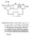
- a video signal v received by a tuner of the television receiver and containing the first and the second fields A and B of each frame in time division is transmitted after passing through an analog-digital converter and the known image processing devices of the television receiver fed to a video memory 100.
- the data buses provided for the signal line are represented by double arrows in FIG. 2a and in the following figures. Their function is known and is therefore not explicitly mentioned.
- the first field A is stored in the video memory (video RAM) 100. While the first field A is being written into the video memory 100, it is read out at a raster frequency of 100 Hz and the primary first field A is displayed on the screen.
- the second field B of the first frame following the first field A of the first frame is simultaneously led to the video memory 100 and to a first input of a detector 110.
- the first field A of the first frame which is delayed by one field from the memory 100, is present at a second input of the detector 110.
- the detector 110 described in more detail below determine, by line-by-line comparison of the luminance signals of one line of the first field A and the corresponding vertical-temporally following line of the second field B, the step amplitude by forming the difference between the individual luminance values.
- the difference signals detected by the detector 110 are converted into corresponding correction values. These are stored in a RAM correction value memory 120.
- the RAM correction value memory 120 is physically separate from the video memory 100. However, it is also possible to dimension the video memory 100 such that both a field and the correction values supplied by the detector 110 can be stored in it.
- the correction values temporarily stored in the correction value memory 120 are sent to a correction device 130 (cf. FIG. 7), at the output of which the corrected video signal v 'with suppressed surface flickering and edge flicker can be tapped.
- the described signal-adaptive deceleration or acceleration of fields or of lines or of line contents is merely a way of expression which is based on the appearance of the disturbing edge flickering of horizontal contrast transitions leans on.
- Any intermediate values can be formed by means of the correction device 130, which is fed with the associated correction value from the detector 110.
- the correction values stored in the correction value memory 120 are thus directly related to the individual pixels and not to lines or even fields.
- the time sequence of the correction of the first and second fields A and B of each frame carried out in the correction device 130 is shown schematically in FIG. 2b.
- the first line schematically shows the chronological sequence of the first and second fields 1A and 1B of the first frame and of the first and second fields 2A, 2B, 3A, 3B of the second and third frames, with a vertical frequency of 50 Hz at the input of the device. Accordingly, the length of a section of the first three lines corresponds to a time span of 20 ms.
- the individual sections of the last two lines of FIG. 2b represent a time span of 10 ms.
- the line in FIG. 2b shows the chronological sequence of the fields present at the second input of the detector 110.
- the third line in FIG. 2a schematically shows the sequence of the correction values K1B, K2A, K2B, K3A and K3B found in the detector 110.
- the fourth line shows the time sequence for the correction of the individual fields by a signal-adaptive delay.
- the further course of the correction of the television pictures to eliminate the edge flickering by a signal-adaptive delay of the The corresponding primary field can be seen in FIG. 2b and is therefore no longer explicitly listed here.
- the double arrow or the single arrow in FIG. 2b indicates the primary first and second fields A, B to be delayed.
- the correction of the edge flickering by the above-described signal-adaptive acceleration of the temporally following secondary field is shown in the fifth line of FIG. 2b. If a signal jump is first detected in the first field 1A with respect to the second field 1B, the secondary second field 1B 'is signal-adaptively accelerated. The further course of the corrections for reducing the edge flickering due to the signal-adaptive acceleration of a corresponding field can also be seen in FIG. 2b and is therefore no longer explained explicitly.
- the single arrow in FIG. 2b points to the secondary first and second fields A ', B' to be accelerated: At this point it should be stated that an "acceleration" of a field cannot be achieved from a technical point of view.
- These measures result in an acceleration of the relevant field.
- additional devices (not shown here) are to be provided for this.
- the delay time is controlled by the correction device. For example, in the "normal case” the video signal is delayed exactly by one line, with “acceleration” the delay is canceled and with “delay” the delay time is increased by the duration of another line.
- FIG. 3a A second exemplary embodiment of a device is shown in FIG. 3a.
- the detector 110 and the correction device 130 this also has a further video memory 100 '.
- the storage capacity of the further video memory 100 ' is selected such that a half field can be stored in it.
- the first field A stored in the video memory 100 is supplied to the detector 110 and the correction device 130 at the same time, delayed by one field.
- the line-by-line determination of the phase and the amount of the jump amplitude by comparing the first field A delayed by one field and the second field B applied to the first input of the detector 110.
- the correction values provided by the detector 110 are stored in the correction device 130 processed.
- the essential difference between the second exemplary embodiment described here and the first exemplary embodiment explained above is that the correction values are not stored in a correction value memory 120. Rather, it is provided that the correction device 130 links the correction values directly to the first field A read from the video memory 100 and fed to the correction device 130 and corrects it accordingly. The corrected first field A is then temporarily stored in the further video memory 100 '. The image information contained in the video memory 100 and in the further video memory 100 ′ is read out alternately by means of a multiplexer 140.
- the time sequence of the method steps is again shown in Fig. 3b.
- the first line shows the chronological order of those received by the television receiver Fields 1A and 1B of the first frame and the corresponding first and second fields 2A, 2B, 3A, 3B, etc. of the second and subsequent frames.
- the second line shows the signal sequence of the first and second fields applied to the detector 110 and delayed by one field from the video memory 100.
- the third line of FIG. 2b shows the image information contained in the further video memory 100 '.
- Lines 4 and 5 show the alternating readout of the signal-adaptively delayed or signal-adaptively accelerated fields from the video memory 100 (line 4) and from the further video memory 100 '(line 5).
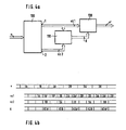
- FIG. 4a shows a preferred third exemplary embodiment of the device.
- This has a video memory 100 which is dimensioned in this way. that two full fields can be stored in it.
- the fields A and B recorded in the video memory 100 are read out simultaneously at a raster frequency of 100 Hz via the outputs 1, 2 and fed to the detector 110.
- the corresponding field vz1 originating from the first output 1 is corrected.
- This device has the advantage that the correction values K or the corrected field v 'no longer have to be buffered. Rather, the signal vz1 read out from the video memory 100 is written on the screen in the correction device 130 immediately after the signal-adaptive correction.
- the fourth line K indicates which of the fields originating from the first output 1 is corrected.
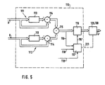
- FIG. 5 shows a first embodiment of the detector 110.
- the current field present at the first input of the detector for example A, is passed to a first differentiator 111.
- the field, for example B, read from the video memory 100 and directed to the second input of the detector 110 is connected to a second differentiator 112 comparative fields A, B.
- Each differentiating element 111 or 112 consists of a delay line 113 and a subtractor 114.
- the field present at the input of each differentiating element is passed directly to the subtractor 114 once and once via the delay line 113, which causes a delay by one line.
- the luminance signal of a line is differentiated in a known manner.
- the output signals of the two differentiators 111 and 112 are passed to a further subtractor 115.
- the further subtractor 115 the difference signal essential for the detection of a signal jump is formed.
- the difference signal is passed to a computing device 116, which is controlled by a control device 117 of the detector 110. It is provided here that a control signal, for example the sign position, is decoupled from the difference signal of two corresponding lines formed in the further subtractor 115, the signal information of which contains the phase of the difference signal. This is about the Signal line 119 passed to control device 117.
- signals are supplied to the control device 117 via further signal lines 118 and 118 'from a central control device (not shown) of the television receiver, which contains information about the fields present on the differentiators 111 and 112 (first or second or primary or secondary field).
- the control device 117 controls the computing device 116 via the additional signal line 116 ′ in accordance with the method sequence described at the beginning, in which the correction values already described, for example as two's complement binary numbers, are calculated.
- a signal line 121 connects the control device 117 to the RAM correction value memory 120, in which the correction values supplied by the computing device 116 are stored.
- the control device 117 - as described in the second exemplary embodiment - may be connected directly to the correction device 130 via the signal line 121.
- the value of the output signals of further subtraction 115 may be inverted by means of the computing device 116, the inversion being dependent on the respective field phase A, A ', B', B.
- FIG. 6 shows a second embodiment of the detector 110 shown, which is predestined in a particularly advantageous manner for use in a device corresponding to the third embodiment.
- the components already known from FIG. 5 are provided with the same reference symbols, which is why they are no longer described here.
- the essential difference of this second embodiment of the detector 110 from the previously described first embodiment is that the detector 110 simultaneously via the data buses D1, D2, D3 the current field, a further field delayed by 313 lines - i.e. by one field - and one third field delayed by 625 lines - that is, one frame. It is essential here that the information just given about the delay times relates to the fields read out at a raster frequency of 100 Hz and not to the fields present at the input of video memory 100 with a vertical frequency of 50 Hz.
- the mode of operation of this detector can be seen from the time sequence of the signal processing of the third exemplary embodiment shown in FIG. 4b.
- the detector 110 receives this from the video memory 100 via the data bus D1 read out field currently to be written on the screen - for example the primary second field 2A - supplied. Accordingly, the primary second field 1B is present over the data bus D2 and the secondary second field 1B 'is present over the data bus D3.
- the control device 117 of the detector 110 determines on the basis of the information supplied by the central control device of the television receiver via the signal lines 118 and 118 'which of the three fields applied to the detector 110 are to be compared.
- the edge flicker is detected by comparing the fields 2A and 1B led to the detector 110 via the data buses D1 and D2. Accordingly, the difference signal formed in the first further subtractor 115 from the luminance signals is passed to the computing device 116 via an electronic data switch contained in the control device 117. The inverted or non-inverted correction values calculated therein are fed to a correction value memory 120 or directly to the correction device 130.
- the secondary first field 2A ', the primary first field 2A and the secondary second field 1B are fed to the detector 110 via the data buses D1, D2 and D3. Because the primary and the secondary first Fields 2A and 2A 'have identical image information, in this case the detection of the edge flicker must be carried out by comparing the fields 2A' and 1B applied to the data buses D1 and D3. In this case, the control device 117 only forwards the difference signal of the secondary first field 2A ′ and the primary second field 1B obtained in the second further subtractor 115 ′ to the computing device 116.
- the further process steps in the detection of edge flickering of the following fields can be seen from the explanations just made.
- FIG. 1 An exemplary embodiment of the correction device 130 is shown schematically as a block diagram in FIG. This is a circuit for linear interpolation in the vertical direction.
- the field to be corrected is passed via a data bus D4 to a delay line 131, to a subtractor 132 and to a summer 134.
- the delay line 131 the field is delayed by one line and then passed to the minuend input 132 ′′ of the subtractor 132.
- the undelayed field is present at the subtrahend input 132 'of the subtractor 132.
- Luminance signals form a difference signal which is fed to a multiplier 133.
- the difference signal is multiplied pixel by pixel by a correction factor kf, which is formed from the corresponding correction values k obtained by the detector 110.
- the correction values stored in the correction value memory 120 are weighted by means of an evaluation circuit 135 with, in particular, a non-linear evaluation characteristic, cf.
- a non-linear evaluation characteristic cf.
- the dash-dotted line applies when the evaluation circuit 135 operates in strictly proportional fashion, so that the correction values k are passed through unchanged to the multiplier 133.
- the difference signal multiplied by the corresponding correction factors kf is passed to a first input of a summer 134, at whose second input the undelayed field is present.
Landscapes
- Engineering & Computer Science (AREA)
- Multimedia (AREA)
- Signal Processing (AREA)
- Television Systems (AREA)
- Picture Signal Circuits (AREA)
Priority Applications (5)
| Application Number | Priority Date | Filing Date | Title |
|---|---|---|---|
| DE59008311T DE59008311D1 (de) | 1990-03-09 | 1990-03-09 | Verfahren und Vorrichtung zur Reduktion des Kantenflackerns eines Fernsehbildes. |
| EP90104483A EP0445336B1 (fr) | 1990-03-09 | 1990-03-09 | Méthode et dispositif de réduction du scintillement du bord d'une image de télévision |
| US07/662,647 US5146329A (en) | 1990-03-09 | 1991-03-01 | Apparatus and method for reducing line flicker in a television picture |
| JP3067888A JPH04220089A (ja) | 1990-03-09 | 1991-03-07 | テレビ画像におけるエッジフリッカーを減少するための方法及び装置 |
| KR1019910003709A KR910017838A (ko) | 1990-03-09 | 1991-03-08 | 텔레비전 화상의 에지 플리커를 감소시키는 방법 및 장치 |
Applications Claiming Priority (1)
| Application Number | Priority Date | Filing Date | Title |
|---|---|---|---|
| EP90104483A EP0445336B1 (fr) | 1990-03-09 | 1990-03-09 | Méthode et dispositif de réduction du scintillement du bord d'une image de télévision |
Publications (2)
| Publication Number | Publication Date |
|---|---|
| EP0445336A1 true EP0445336A1 (fr) | 1991-09-11 |
| EP0445336B1 EP0445336B1 (fr) | 1995-01-18 |
Family
ID=8203733
Family Applications (1)
| Application Number | Title | Priority Date | Filing Date |
|---|---|---|---|
| EP90104483A Expired - Lifetime EP0445336B1 (fr) | 1990-03-09 | 1990-03-09 | Méthode et dispositif de réduction du scintillement du bord d'une image de télévision |
Country Status (5)
| Country | Link |
|---|---|
| US (1) | US5146329A (fr) |
| EP (1) | EP0445336B1 (fr) |
| JP (1) | JPH04220089A (fr) |
| KR (1) | KR910017838A (fr) |
| DE (1) | DE59008311D1 (fr) |
Cited By (1)
| Publication number | Priority date | Publication date | Assignee | Title |
|---|---|---|---|---|
| CN108111767A (zh) * | 2018-01-24 | 2018-06-01 | 努比亚技术有限公司 | 一种拍摄方法、终端及计算机可读存储介质 |
Families Citing this family (21)
| Publication number | Priority date | Publication date | Assignee | Title |
|---|---|---|---|---|
| JP2585957B2 (ja) | 1992-08-18 | 1997-02-26 | 富士通株式会社 | ビデオデータ変換処理装置とビデオデータ変換装置を有する情報処理装置 |
| US5510843A (en) * | 1994-09-30 | 1996-04-23 | Cirrus Logic, Inc. | Flicker reduction and size adjustment for video controller with interlaced video output |
| US5611041A (en) * | 1994-12-19 | 1997-03-11 | Cirrus Logic, Inc. | Memory bandwidth optimization |
| WO1997005598A1 (fr) * | 1995-07-27 | 1997-02-13 | Magix | Systeme pour diminuer le scintillement dans l'affichage entrelace d'un ordinateur graphique |
| JP3717590B2 (ja) * | 1996-03-08 | 2005-11-16 | フジノン株式会社 | プロンプターの映像信号処理装置 |
| US5929935A (en) * | 1996-12-02 | 1999-07-27 | Motorola, Inc. | Method for reducing flicker and circuit therefor |
| US5963262A (en) * | 1997-06-30 | 1999-10-05 | Cirrus Logic, Inc. | System and method for scaling images and reducing flicker in interlaced television images converted from non-interlaced computer graphics data |
| US6108041A (en) * | 1997-10-10 | 2000-08-22 | Faroudja Laboratories, Inc. | High-definition television signal processing for transmitting and receiving a television signal in a manner compatible with the present system |
| US6014182A (en) * | 1997-10-10 | 2000-01-11 | Faroudja Laboratories, Inc. | Film source video detection |
| US6130723A (en) * | 1998-01-15 | 2000-10-10 | Innovision Corporation | Method and system for improving image quality on an interlaced video display |
| US6421097B1 (en) | 1998-07-31 | 2002-07-16 | Intel Corporation | Method and apparatus for reducing flicker in a video image sequence |
| US7119853B1 (en) | 1999-07-15 | 2006-10-10 | Sharp Laboratories Of America, Inc. | Method of eliminating flicker on an interlaced monitor |
| US6650372B2 (en) * | 2001-01-22 | 2003-11-18 | Sony Corporation | Dynamic change of flicker filter |
| TW561783B (en) * | 2002-03-12 | 2003-11-11 | Via Tech Inc | Image processing method and device |
| TW527824B (en) * | 2002-03-12 | 2003-04-11 | Via Tech Inc | Adative-deflicker processing method and adaptive deflicker filter |
| TW563353B (en) * | 2002-03-12 | 2003-11-21 | Via Tech Inc | Clock signal synthesizer with multiple frequency outputs and method for synthesizing clock signal |
| US6816535B2 (en) * | 2002-09-17 | 2004-11-09 | Northrop Grumman Corporation | Co-alignment of time-multiplexed pulsed laser beams to a single reference point |
| DE102007015320B4 (de) * | 2006-11-03 | 2008-10-23 | Basler Ag | Kamera zur Analyse von Objekten |
| JP5219609B2 (ja) * | 2008-05-01 | 2013-06-26 | キヤノン株式会社 | フレームレート変換装置、方法及びプログラム |
| JP5596943B2 (ja) * | 2009-07-09 | 2014-09-24 | キヤノン株式会社 | 画像表示装置及びその制御方法 |
| CN110445952B (zh) * | 2019-07-15 | 2021-12-21 | 浙江大华技术股份有限公司 | 摄像头的画面闪烁处理方法、装置、设备和存储介质 |
Citations (2)
| Publication number | Priority date | Publication date | Assignee | Title |
|---|---|---|---|---|
| EP0305017A2 (fr) * | 1987-08-26 | 1989-03-01 | Bang & Olufsen A/S | Récepteur de télévision comportant un dispositif de suppression de scintillement des lignes |
| EP0318760A2 (fr) * | 1987-12-02 | 1989-06-07 | Blaupunkt-Werke GmbH | Récepteur de télévision avec un dispositif de suppression des perturbations de scintillement |
Family Cites Families (4)
| Publication number | Priority date | Publication date | Assignee | Title |
|---|---|---|---|---|
| NL7900324A (nl) * | 1979-01-16 | 1980-07-18 | Philips Nv | Rasterinterpolatieschakeling. |
| NL8501582A (nl) * | 1985-02-12 | 1986-09-01 | Philips Nv | Videosignaalverwerkingsschakeling voor de verwerking van een geinterlinieerd videosignaal. |
| US4680632A (en) * | 1985-07-31 | 1987-07-14 | Rca Corporation | Television display system with flicker reduction processor having burst locked clock and skew correction |
| DE3740826A1 (de) * | 1987-12-02 | 1989-06-15 | Blaupunkt Werke Gmbh | Fernsehempfaenger mit einer einrichtung zur unterdrueckung von flimmerstoerungen |
-
1990
- 1990-03-09 EP EP90104483A patent/EP0445336B1/fr not_active Expired - Lifetime
- 1990-03-09 DE DE59008311T patent/DE59008311D1/de not_active Expired - Fee Related
-
1991
- 1991-03-01 US US07/662,647 patent/US5146329A/en not_active Expired - Fee Related
- 1991-03-07 JP JP3067888A patent/JPH04220089A/ja active Pending
- 1991-03-08 KR KR1019910003709A patent/KR910017838A/ko not_active Withdrawn
Patent Citations (2)
| Publication number | Priority date | Publication date | Assignee | Title |
|---|---|---|---|---|
| EP0305017A2 (fr) * | 1987-08-26 | 1989-03-01 | Bang & Olufsen A/S | Récepteur de télévision comportant un dispositif de suppression de scintillement des lignes |
| EP0318760A2 (fr) * | 1987-12-02 | 1989-06-07 | Blaupunkt-Werke GmbH | Récepteur de télévision avec un dispositif de suppression des perturbations de scintillement |
Cited By (2)
| Publication number | Priority date | Publication date | Assignee | Title |
|---|---|---|---|---|
| CN108111767A (zh) * | 2018-01-24 | 2018-06-01 | 努比亚技术有限公司 | 一种拍摄方法、终端及计算机可读存储介质 |
| CN108111767B (zh) * | 2018-01-24 | 2020-07-28 | 努比亚技术有限公司 | 一种拍摄方法、终端及计算机可读存储介质 |
Also Published As
| Publication number | Publication date |
|---|---|
| EP0445336B1 (fr) | 1995-01-18 |
| DE59008311D1 (de) | 1995-03-02 |
| KR910017838A (ko) | 1991-11-05 |
| JPH04220089A (ja) | 1992-08-11 |
| US5146329A (en) | 1992-09-08 |
Similar Documents
| Publication | Publication Date | Title |
|---|---|---|
| EP0445336B1 (fr) | Méthode et dispositif de réduction du scintillement du bord d'une image de télévision | |
| DE69513370T2 (de) | Unterdrückung von sägezahnstörungen bei der anzeige eines fernsehsignals mit progressiver zeilenstruktur | |
| DE69637276T2 (de) | Bildanzeigegerät | |
| DE68915912T2 (de) | Videosignalerzeugung als Zeitlupenaufnahme. | |
| DE69506076T2 (de) | Umsetzung einer zeilensprung-abtastung in eine sequentielle abtastung | |
| DE69422255T2 (de) | Verfahren und Vorrichtung zum bewegungsausgeglichenen Interpolieren von zwischenliegenden Halbbildern oder Bildern | |
| DE69608785T2 (de) | Verfahren zur verbesserung der vertikalen auflosung eines fernsehsignals mit verminderten vertikalen chominanzubergangen | |
| DE3134703C2 (fr) | ||
| DE3244808A1 (de) | Fernsehempfaenger, bei dem das fernsehbild nicht nach dem zwischenzeilenverfahren wiedergegeben wird | |
| EP0318757A2 (fr) | Récepteur de télévision avec un dispositif de suppression des perturbations de scintillement | |
| EP0564957A2 (fr) | Méthode et dispositif de conversion entrelacé-progressif | |
| DE3330570A1 (de) | Doppelabtastender zeilensprungfreier fernsehempfaenger | |
| DE69830471T2 (de) | Interpolator mit einem gewichteten Medianfilter | |
| DE69120770T2 (de) | Fortlaufendes Fernsehen für Mehrfarbnormen | |
| DE69420085T2 (de) | Fernsehempfänger | |
| EP1125428B1 (fr) | Circuit permettant de transformer un debit binaire | |
| EP0318760A2 (fr) | Récepteur de télévision avec un dispositif de suppression des perturbations de scintillement | |
| EP0370500B1 (fr) | Dispositif de circuit de sélection entre différentes méthodes de réduction du papillotement dans un récepteur de télévision | |
| EP0596561B1 (fr) | Dispositif de doublement de la fréquence de trame d'un signal d'image | |
| EP0739130B1 (fr) | Procédé et circuit d'insertion d'image dans l'image | |
| EP0431116B1 (fr) | Circuit pour reduire le sautillement au niveau des lignes et des contours dans des images de television, et circuit d'interpolation | |
| EP0705031B1 (fr) | Procédé et circuit pour réduire le scintillement pour un dispositif de traitement signal vidéo | |
| DE69519097T2 (de) | Bewegungsdetektor für Videosignale mit Zeilensprung | |
| EP0753972A2 (fr) | Procédé d'interpolation intertrame de signaux de différence de couleur et circuit pour la réalisation du procédé | |
| DE4414173C1 (de) | Verfahren zur Umsetzung einer Bildfolge von Halbbildern mit Zeilensprung auf eine Bildfolge von zeilensprungfreien Bildern und Schaltungsanordnung zur Durchführung des Verfahrens |
Legal Events
| Date | Code | Title | Description |
|---|---|---|---|
| PUAI | Public reference made under article 153(3) epc to a published international application that has entered the european phase |
Free format text: ORIGINAL CODE: 0009012 |
|
| 17P | Request for examination filed |
Effective date: 19910104 |
|
| AK | Designated contracting states |
Kind code of ref document: A1 Designated state(s): DE FR GB IT NL |
|
| 17Q | First examination report despatched |
Effective date: 19930629 |
|
| GRAA | (expected) grant |
Free format text: ORIGINAL CODE: 0009210 |
|
| AK | Designated contracting states |
Kind code of ref document: B1 Designated state(s): DE FR GB IT NL |
|
| REF | Corresponds to: |
Ref document number: 59008311 Country of ref document: DE Date of ref document: 19950302 |
|
| ET | Fr: translation filed | ||
| GBT | Gb: translation of ep patent filed (gb section 77(6)(a)/1977) |
Effective date: 19950208 |
|
| ITF | It: translation for a ep patent filed | ||
| PLBE | No opposition filed within time limit |
Free format text: ORIGINAL CODE: 0009261 |
|
| STAA | Information on the status of an ep patent application or granted ep patent |
Free format text: STATUS: NO OPPOSITION FILED WITHIN TIME LIMIT |
|
| 26N | No opposition filed | ||
| PGFP | Annual fee paid to national office [announced via postgrant information from national office to epo] |
Ref country code: FR Payment date: 19990218 Year of fee payment: 10 |
|
| PGFP | Annual fee paid to national office [announced via postgrant information from national office to epo] |
Ref country code: GB Payment date: 19990219 Year of fee payment: 10 |
|
| PGFP | Annual fee paid to national office [announced via postgrant information from national office to epo] |
Ref country code: NL Payment date: 19990222 Year of fee payment: 10 |
|
| PG25 | Lapsed in a contracting state [announced via postgrant information from national office to epo] |
Ref country code: GB Free format text: LAPSE BECAUSE OF NON-PAYMENT OF DUE FEES Effective date: 20000309 |
|
| PG25 | Lapsed in a contracting state [announced via postgrant information from national office to epo] |
Ref country code: NL Free format text: LAPSE BECAUSE OF NON-PAYMENT OF DUE FEES Effective date: 20001001 |
|
| GBPC | Gb: european patent ceased through non-payment of renewal fee |
Effective date: 20000309 |
|
| PG25 | Lapsed in a contracting state [announced via postgrant information from national office to epo] |
Ref country code: FR Free format text: LAPSE BECAUSE OF NON-PAYMENT OF DUE FEES Effective date: 20001130 |
|
| NLV4 | Nl: lapsed or anulled due to non-payment of the annual fee |
Effective date: 20001001 |
|
| REG | Reference to a national code |
Ref country code: FR Ref legal event code: ST |
|
| PG25 | Lapsed in a contracting state [announced via postgrant information from national office to epo] |
Ref country code: IT Free format text: LAPSE BECAUSE OF NON-PAYMENT OF DUE FEES;WARNING: LAPSES OF ITALIAN PATENTS WITH EFFECTIVE DATE BEFORE 2007 MAY HAVE OCCURRED AT ANY TIME BEFORE 2007. THE CORRECT EFFECTIVE DATE MAY BE DIFFERENT FROM THE ONE RECORDED. Effective date: 20050309 |
|
| PGFP | Annual fee paid to national office [announced via postgrant information from national office to epo] |
Ref country code: DE Payment date: 20050502 Year of fee payment: 16 |
|
| PG25 | Lapsed in a contracting state [announced via postgrant information from national office to epo] |
Ref country code: DE Free format text: LAPSE BECAUSE OF NON-PAYMENT OF DUE FEES Effective date: 20061003 |