EP0445384A2 - Procédé et circuit pour le réglage d'un seuil - Google Patents
Procédé et circuit pour le réglage d'un seuil Download PDFInfo
- Publication number
- EP0445384A2 EP0445384A2 EP90123240A EP90123240A EP0445384A2 EP 0445384 A2 EP0445384 A2 EP 0445384A2 EP 90123240 A EP90123240 A EP 90123240A EP 90123240 A EP90123240 A EP 90123240A EP 0445384 A2 EP0445384 A2 EP 0445384A2
- Authority
- EP
- European Patent Office
- Prior art keywords
- reference value
- data signal
- signal
- output
- value
- Prior art date
- Legal status (The legal status is an assumption and is not a legal conclusion. Google has not performed a legal analysis and makes no representation as to the accuracy of the status listed.)
- Granted
Links
Images
Classifications
-
- H—ELECTRICITY
- H04—ELECTRIC COMMUNICATION TECHNIQUE
- H04L—TRANSMISSION OF DIGITAL INFORMATION, e.g. TELEGRAPHIC COMMUNICATION
- H04L1/00—Arrangements for detecting or preventing errors in the information received
- H04L1/20—Arrangements for detecting or preventing errors in the information received using signal quality detector
-
- H—ELECTRICITY
- H04—ELECTRIC COMMUNICATION TECHNIQUE
- H04L—TRANSMISSION OF DIGITAL INFORMATION, e.g. TELEGRAPHIC COMMUNICATION
- H04L25/00—Baseband systems
- H04L25/02—Details ; arrangements for supplying electrical power along data transmission lines
- H04L25/06—DC level restoring means; Bias distortion correction ; Decision circuits providing symbol by symbol detection
- H04L25/061—DC level restoring means; Bias distortion correction ; Decision circuits providing symbol by symbol detection providing hard decisions only; arrangements for tracking or suppressing unwanted low frequency components, e.g. removal of DC offset
Definitions
- the invention relates to a method for level monitoring according to the preamble of claim 1. Circuit arrangements for carrying out this method are specified in the independent claims.
- the object of the invention is to provide a method for level monitoring for a large level range. Suitable arrangements for implementing the method must also be specified.
- the method has the advantage that a reference signal is first derived from the received signal.
- a received Signal is particularly easy to recognize if it is preceded by a special distant signal. This can be, for example, a signal with a predetermined frequency, a so-called alarm tone. But even without a special distant signal, a data signal can be reliably recognized by comparing its main spectrum with the entire received signal.
- a special distant signal can be, for example, a signal with a predetermined frequency, a so-called alarm tone.
- a data signal can be reliably recognized by comparing its main spectrum with the entire received signal.
- the level detection is equipped with a hysteresis. This ensures a high level of reliability for the response of the level monitoring in the case of a large level range.
- An arrangement for carrying out the method can be implemented with conventional circuits such as adders, subtractors, counters, comparators and flip-flops, as well as with a digital computer, for example a microprocessor.
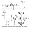
- the basic circuit diagram of the level monitoring shown in FIG. 1 contains a sample and hold circuit 2, the input of which 1 a band-limited data signal s is supplied.
- An analog-to-digital converter 3 connects to the sample and hold circuit, and 4 digital samples x i are output at its output.
- the output 4 is connected to an absolute value formation circuit 5, the output of which is connected directly to a first input of a comparator 11 designed as a subtractor and via a reference value circuit 7 to the subtraction input of the subtractor.
- Only the sign bit sgn is fed from the output of the subtractor to the control input 12 of an up-down counter 14, the output 16 of which is led to two comparators 17 and 18.
- the outputs of the comparators control a flip-flop 19, which outputs a control signal SS at its output 20.
- a sine wave SIN of 10 kHz is transmitted as a distant signal - a so-called alarm tone.
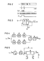
- the distant signal is filtered out in a signal detection circuit (FIG. 4) and, after its reliable detection, the reference value circuit 7 is activated from a time T1 to a time T2.
- the distant signal - like the data DA received later - is sampled and digitized, for example, with a clock frequency of 80 kHz. Then the amounts
- the reference value circuit should form the arithmetic mean here, for example. This is easy to do.
- the reference value circuit consists of an adder AD with a downstream register RE. The samples
- the arithmetic mean multiplied by a normalization factor gives the reference value XR. If the normalization factor is 0.5, for example, only the arithmetic mean is shifted by another binary digit. The reference value remains stored until another warning signal occurs or until the connection is broken.
- the digital sampling values x i must be multiplied with one another, which of course eliminates the need for previous amounts.
- RMS value root mean square
- the up-down counter must have overflow logic, ie it must not count beyond its extreme values, but must block itself. An extreme value can match the comparison value MAX.
- the reference value can be deleted by a reset clock TR1 when a connection is established or a connection is cleared via a reset input 10.
- the up-down counter After the end of the received data block, the samples
- the up-down counter then has five flip-flops.
- the comparators 17 and 18 can be integrated in the counter, for example by means of a gate logic for the extreme values, the carry outputs then directly controlling the RS flip-flop 19 and blocking the operating cycle CLC.
- the counter will quickly return from its minimum value to its maximum value and signal the renewed receipt of a data signal. If, as in the exemplary embodiment according to FIG. 1, only the criteria "greater (or greater and equal and) or less than the reference value" are evaluated, it does not matter for the function whether a conventional comparator or a subtractor 11 is used.
- FIG. 1 An example of a signal detection circuit is given in FIG. This is not part of the invention and is constructed differently in accordance with the different received signals.
- the received signal is applied to a first rectifier circuit 22 via a filter 21, which can be a bandpass filter or an oscillating circuit, for example, and is passed to a first input of a comparator 27 via an average circuit 23.
- the received signal is also passed to a second input of the comparator 27 without special filtering via a second rectifier 24, a second mean value circuit 25 and a voltage divider 26.
- a filter acting as a bandstop can also be used in this circuit branch.
- a timer 28 is switched on at the output of the comparator.
- the timer 28 is activated and supplies a time window signal CS (FIG. 2) between T1 and T2, which activates the reference value circuit, for example by applying a reference clock CLR during the Duration of the time window. If the time window is to include an exact number of work cycles, then a counter controlled by the work cycle CLC is also used as the timing element.
- the average value circuits and the voltage divider can be implemented by the rectifiers charging or discharging a capacitor via different ohmic resistors.
- the signal detection circuit can of course also be carried out digitally.
- a distant signal with constant frequency can be recognized by measuring the period. If several consecutive periods or a predetermined number of measured periods correspond to the period of the warning signal (alarm tone), the time window signal is emitted to determine the reference value.
- the function of the processor PR constructed with hardware in FIG. 1 can also be implemented as a program part in a digital processor.
- the corresponding arrangement is shown in FIG. 5.
- the digital samples x i are fed to a digital processor (microprocessor) 30 via its data input 31.
- a work cycle TA which is fed to its clock input 33, it also requires the time window signal CS to control the formation of the reference value (if it does not also generate this itself).
- the processor can carry out the tasks, such as absolute value formation, determination of the reference value from the arithmetic mean, difference formation or comparison of sample value and reference value, and addition of the comparison result without problems.
- a data output of the processor can be used directly as output 20 of the level monitoring.
- the control signal SS can also be output via a status memory.
Landscapes
- Engineering & Computer Science (AREA)
- Computer Networks & Wireless Communication (AREA)
- Signal Processing (AREA)
- Power Engineering (AREA)
- Quality & Reliability (AREA)
- Dc Digital Transmission (AREA)
- Analogue/Digital Conversion (AREA)
- Monitoring And Testing Of Transmission In General (AREA)
Applications Claiming Priority (2)
| Application Number | Priority Date | Filing Date | Title |
|---|---|---|---|
| DE4007013 | 1990-03-06 | ||
| DE4007013 | 1990-03-06 |
Publications (3)
| Publication Number | Publication Date |
|---|---|
| EP0445384A2 true EP0445384A2 (fr) | 1991-09-11 |
| EP0445384A3 EP0445384A3 (en) | 1992-12-23 |
| EP0445384B1 EP0445384B1 (fr) | 1995-07-26 |
Family
ID=6401528
Family Applications (1)
| Application Number | Title | Priority Date | Filing Date |
|---|---|---|---|
| EP90123240A Expired - Lifetime EP0445384B1 (fr) | 1990-03-06 | 1990-12-04 | Procédé et circuit pour le réglage d'un seuil |
Country Status (5)
| Country | Link |
|---|---|
| US (1) | US5323331A (fr) |
| EP (1) | EP0445384B1 (fr) |
| CA (1) | CA2037484C (fr) |
| DE (1) | DE59009441D1 (fr) |
| IL (1) | IL97338A (fr) |
Families Citing this family (4)
| Publication number | Priority date | Publication date | Assignee | Title |
|---|---|---|---|---|
| DE4421083C2 (de) * | 1994-06-16 | 1996-04-11 | Volkswagen Ag | Verfahren zur Überwachung einer seriellen Übertragung von digitalen Daten auf einer Ein-Draht-Multiplexverbindung zwischen untereinander kommunizierenden Signalverarbeitungsgeräten |
| US6683530B1 (en) * | 1999-09-08 | 2004-01-27 | Sun Microsystems, Inc. | Method and apparatus for performing a floating point compare operation |
| EP1176750A1 (fr) * | 2000-07-25 | 2002-01-30 | Telefonaktiebolaget L M Ericsson (Publ) | Détermination de la qualité de liaison d'un canal de transmission dans un système de transmission de OFDM |
| US9035636B2 (en) * | 2013-09-17 | 2015-05-19 | Power Integrations, Inc. | Digital peak detector with follower mode |
Family Cites Families (16)
| Publication number | Priority date | Publication date | Assignee | Title |
|---|---|---|---|---|
| NL124462C (fr) * | 1960-06-09 | 1968-07-15 | ||
| DE1292181C2 (de) * | 1963-12-28 | 1974-09-19 | Fujitsu Ltd Comm And Electroni | Verfahren und Schaltungsanordnung zum UEberwachen, Pruefen und/oder Erkennen elektrischer Impulse binaercodierter Informationen |
| DE1189119B (de) * | 1964-02-22 | 1965-03-18 | Telefunken Patent | Verfahren und Anordnung zur Pruefung von Datenuebertragungen auf Stoerungsfreiheit |
| DE1202313B (de) * | 1964-02-28 | 1965-10-07 | Telefunken Patent | Verfahren zur Pruefung von Datenuebertragungen auf Stoerungsfreiheit |
| SE220523C1 (fr) * | 1964-05-28 | 1968-05-14 | ||
| DE1227501B (de) * | 1965-01-20 | 1966-10-27 | Telefunken Patent | Verfahren zur Pruefung von Datenuebertragungen auf Stoerungsfreiheit |
| US3683367A (en) * | 1970-02-12 | 1972-08-08 | Datamax Corp | Digital automatic gain control |
| US3858199A (en) * | 1973-01-03 | 1974-12-31 | Westinghouse Electric Corp | Tracking level detector |
| JPS56136050A (en) * | 1980-03-28 | 1981-10-23 | Nec Corp | Individual selective call reception system |
| JPS5767322A (en) * | 1980-10-15 | 1982-04-23 | Fujitsu Ltd | Analogue-digital converting circuit provided with agc function |
| US4564804A (en) * | 1981-06-08 | 1986-01-14 | Tektronix, Inc. | Method and apparatus for automatically detecting signal levels |
| US4458206A (en) * | 1981-12-21 | 1984-07-03 | Motorola, Inc. | Circuit for synchronizing the demodulation of phase modulated transmission bursts |
| US4558232A (en) * | 1982-02-22 | 1985-12-10 | Simpson Richard D | Level detector circuit for microcomputer devices |
| DE3214574C2 (de) * | 1982-04-20 | 1986-08-21 | Siemens AG, 1000 Berlin und 8000 München | Schaltungsanordnung zum Ermitteln der in der Gesamtdauer eine vorgegebene Dauer überschreitenden Abgabe von Datensignalen |
| JP2533062Y2 (ja) * | 1987-07-03 | 1997-04-16 | ヤマハ株式会社 | アナログディジタル変換回路 |
| JPH0754335B2 (ja) * | 1989-01-31 | 1995-06-07 | 富士通株式会社 | ピーク値検出回路 |
-
1990
- 1990-12-04 EP EP90123240A patent/EP0445384B1/fr not_active Expired - Lifetime
- 1990-12-04 DE DE59009441T patent/DE59009441D1/de not_active Expired - Lifetime
-
1991
- 1991-02-22 IL IL9733891A patent/IL97338A/en not_active IP Right Cessation
- 1991-03-04 CA CA002037484A patent/CA2037484C/fr not_active Expired - Fee Related
-
1993
- 1993-11-04 US US08/145,671 patent/US5323331A/en not_active Expired - Lifetime
Also Published As
| Publication number | Publication date |
|---|---|
| IL97338A (en) | 1994-01-25 |
| US5323331A (en) | 1994-06-21 |
| IL97338A0 (en) | 1992-05-25 |
| CA2037484C (fr) | 2000-09-19 |
| DE59009441D1 (de) | 1995-08-31 |
| EP0445384A3 (en) | 1992-12-23 |
| EP0445384B1 (fr) | 1995-07-26 |
| CA2037484A1 (fr) | 1991-09-07 |
Similar Documents
| Publication | Publication Date | Title |
|---|---|---|
| DE4403910C2 (de) | Verfahren und Vorrichtung zur Generierung von Schwellwertpegeln in einer Funkkommunikationsvorrichtung zum Empfang von Signalen mit vier Pegeln | |
| DE2648977B2 (de) | Demodulator für differentiell phasencodierte Digitaldaten | |
| DE546339T1 (de) | Verteiltes Steuersystem. | |
| DE2323959C3 (de) | Anordnung zur Fernablesung mehrerer Zähler | |
| EP0231786B1 (fr) | Procédé pour éliminer des perturbations dans un signal de mesure | |
| DE3329242A1 (de) | Schaltungsanordnung zum ueberpruefen des zeitlichen abstands von rechtecksignalen | |
| DE69008038T2 (de) | Schaltungsanordnung zur Detektion des Verlustes eines digitalen, empfangenen Signals für digitale Signalempfänger. | |
| DE69012446T2 (de) | Detektor für Niederfrequenz-Wechselstromsignale für eine Telefonverbindungsleitung. | |
| EP0308650A2 (fr) | Méthode et dispositif pour réduire l'horloge de mot des signaux modulés par la disposition des impulsions | |
| EP0445384A2 (fr) | Procédé et circuit pour le réglage d'un seuil | |
| DE3533467C2 (de) | Verfahren und Anordnung zum störsicheren Erkennen von in Datensignalen enthaltenen Daten | |
| DE2628472C3 (de) | Digitale Knackgeräuschunterdrückungsund Rauschsperrensteuerschaltung | |
| DE69028326T2 (de) | Signal-Pegel-Erkennungsschaltkreise | |
| DE2657915C3 (de) | Verfahren und Vorrichtung zur digitalen Messung analoger Größen | |
| DE2824565A1 (de) | Schaltungsanordnung zum erkennen einer frequenz in einem pcm-signal | |
| DE3007294C2 (de) | Schaltungsanordnung zur Demodulation von freqenzumgetasteten Signalen | |
| DE3021485C2 (de) | Verfahren und Schaltungsanordnung zur Trägerfrequenzüberwachung in einem Nachrichtenübertragungssystem | |
| DE68920953T2 (de) | Anordnung mit einer verbesserten Gleichstrompegelauswertungsvorrichtung. | |
| DE2703570A1 (de) | Digital-analog-umsetzer | |
| DE3617949C2 (fr) | ||
| EP0159650B2 (fr) | Dispositif d'évaluation des signaux reçus dans un récepteur de télécommande centralisée à audio-fréquence | |
| DE4328971A1 (de) | Verfahren zur empfangsseitigen Detektierung einer über eine Verbindungsleitung übertragenen Signalwechselspannung | |
| DE3041954A1 (de) | Analog-digital-umsetzer | |
| EP0629048A2 (fr) | Agencement de conversion analogique-numérique de signaux de niveaux différents | |
| DE2811009C2 (de) | Schaltanordnung zum Ermitteln von Über-und Unterschreitungen von Meßwertbereichen eines Analogdigitalwandlers |
Legal Events
| Date | Code | Title | Description |
|---|---|---|---|
| PUAI | Public reference made under article 153(3) epc to a published international application that has entered the european phase |
Free format text: ORIGINAL CODE: 0009012 |
|
| 17P | Request for examination filed |
Effective date: 19901220 |
|
| AK | Designated contracting states |
Kind code of ref document: A2 Designated state(s): BE DE FR GB IT NL SE |
|
| PUAL | Search report despatched |
Free format text: ORIGINAL CODE: 0009013 |
|
| AK | Designated contracting states |
Kind code of ref document: A3 Designated state(s): BE DE FR GB IT NL SE |
|
| 17Q | First examination report despatched |
Effective date: 19940914 |
|
| GRAA | (expected) grant |
Free format text: ORIGINAL CODE: 0009210 |
|
| AK | Designated contracting states |
Kind code of ref document: B1 Designated state(s): BE DE FR GB IT NL SE |
|
| PG25 | Lapsed in a contracting state [announced via postgrant information from national office to epo] |
Ref country code: BE Effective date: 19950726 Ref country code: NL Free format text: LAPSE BECAUSE OF NON-PAYMENT OF DUE FEES Effective date: 19950726 |
|
| REF | Corresponds to: |
Ref document number: 59009441 Country of ref document: DE Date of ref document: 19950831 |
|
| ITF | It: translation for a ep patent filed | ||
| GBT | Gb: translation of ep patent filed (gb section 77(6)(a)/1977) |
Effective date: 19951010 |
|
| ET | Fr: translation filed | ||
| NLV1 | Nl: lapsed or annulled due to failure to fulfill the requirements of art. 29p and 29m of the patents act | ||
| PLBE | No opposition filed within time limit |
Free format text: ORIGINAL CODE: 0009261 |
|
| STAA | Information on the status of an ep patent application or granted ep patent |
Free format text: STATUS: NO OPPOSITION FILED WITHIN TIME LIMIT |
|
| 26N | No opposition filed | ||
| PGFP | Annual fee paid to national office [announced via postgrant information from national office to epo] |
Ref country code: SE Payment date: 20011219 Year of fee payment: 12 |
|
| REG | Reference to a national code |
Ref country code: GB Ref legal event code: IF02 |
|
| PG25 | Lapsed in a contracting state [announced via postgrant information from national office to epo] |
Ref country code: SE Free format text: LAPSE BECAUSE OF NON-PAYMENT OF DUE FEES Effective date: 20021205 |
|
| EUG | Se: european patent has lapsed | ||
| PGFP | Annual fee paid to national office [announced via postgrant information from national office to epo] |
Ref country code: GB Payment date: 20031126 Year of fee payment: 14 |
|
| PGFP | Annual fee paid to national office [announced via postgrant information from national office to epo] |
Ref country code: FR Payment date: 20031209 Year of fee payment: 14 |
|
| PG25 | Lapsed in a contracting state [announced via postgrant information from national office to epo] |
Ref country code: GB Free format text: LAPSE BECAUSE OF NON-PAYMENT OF DUE FEES Effective date: 20041204 |
|
| GBPC | Gb: european patent ceased through non-payment of renewal fee |
Effective date: 20041204 |
|
| PG25 | Lapsed in a contracting state [announced via postgrant information from national office to epo] |
Ref country code: FR Free format text: LAPSE BECAUSE OF NON-PAYMENT OF DUE FEES Effective date: 20050831 |
|
| REG | Reference to a national code |
Ref country code: FR Ref legal event code: ST |
|
| PG25 | Lapsed in a contracting state [announced via postgrant information from national office to epo] |
Ref country code: IT Free format text: LAPSE BECAUSE OF NON-PAYMENT OF DUE FEES;WARNING: LAPSES OF ITALIAN PATENTS WITH EFFECTIVE DATE BEFORE 2007 MAY HAVE OCCURRED AT ANY TIME BEFORE 2007. THE CORRECT EFFECTIVE DATE MAY BE DIFFERENT FROM THE ONE RECORDED. Effective date: 20051204 |
|
| PGFP | Annual fee paid to national office [announced via postgrant information from national office to epo] |
Ref country code: DE Payment date: 20100216 Year of fee payment: 20 |
|
| PG25 | Lapsed in a contracting state [announced via postgrant information from national office to epo] |
Ref country code: DE Free format text: LAPSE BECAUSE OF EXPIRATION OF PROTECTION Effective date: 20101204 |