EP0445883B1 - Method of producing a thin-film magnetic head as well as a thin-film magnetic head producible by means of the method - Google Patents
Method of producing a thin-film magnetic head as well as a thin-film magnetic head producible by means of the method Download PDFInfo
- Publication number
- EP0445883B1 EP0445883B1 EP91200453A EP91200453A EP0445883B1 EP 0445883 B1 EP0445883 B1 EP 0445883B1 EP 91200453 A EP91200453 A EP 91200453A EP 91200453 A EP91200453 A EP 91200453A EP 0445883 B1 EP0445883 B1 EP 0445883B1
- Authority
- EP
- European Patent Office
- Prior art keywords
- layer
- magnetic
- flux conductors
- photolacquer
- magnetic layer
- Prior art date
- Legal status (The legal status is an assumption and is not a legal conclusion. Google has not performed a legal analysis and makes no representation as to the accuracy of the status listed.)
- Expired - Lifetime
Links
- 230000005291 magnetic effect Effects 0.000 title claims description 99
- 238000000034 method Methods 0.000 title claims description 52
- 239000010409 thin film Substances 0.000 title claims description 19
- 239000004020 conductor Substances 0.000 claims description 56
- 230000004907 flux Effects 0.000 claims description 54
- 238000000151 deposition Methods 0.000 claims description 24
- 238000009713 electroplating Methods 0.000 claims description 22
- 238000007747 plating Methods 0.000 claims description 10
- 230000008021 deposition Effects 0.000 claims description 4
- 230000015572 biosynthetic process Effects 0.000 claims description 3
- 239000013067 intermediate product Substances 0.000 description 7
- ZOKXTWBITQBERF-UHFFFAOYSA-N Molybdenum Chemical compound [Mo] ZOKXTWBITQBERF-UHFFFAOYSA-N 0.000 description 5
- 229910052750 molybdenum Inorganic materials 0.000 description 5
- 239000011733 molybdenum Substances 0.000 description 5
- VYPSYNLAJGMNEJ-UHFFFAOYSA-N silicon dioxide Inorganic materials O=[Si]=O VYPSYNLAJGMNEJ-UHFFFAOYSA-N 0.000 description 5
- 239000000758 substrate Substances 0.000 description 5
- 238000005229 chemical vapour deposition Methods 0.000 description 4
- 238000005530 etching Methods 0.000 description 4
- 239000000463 material Substances 0.000 description 4
- 238000004544 sputter deposition Methods 0.000 description 4
- 229910001030 Iron–nickel alloy Inorganic materials 0.000 description 3
- OKTJSMMVPCPJKN-UHFFFAOYSA-N Carbon Chemical compound [C] OKTJSMMVPCPJKN-UHFFFAOYSA-N 0.000 description 2
- 229910052799 carbon Inorganic materials 0.000 description 2
- 229910052681 coesite Inorganic materials 0.000 description 2
- 229910052906 cristobalite Inorganic materials 0.000 description 2
- 239000000945 filler Substances 0.000 description 2
- 239000010408 film Substances 0.000 description 2
- 238000000227 grinding Methods 0.000 description 2
- 239000000696 magnetic material Substances 0.000 description 2
- 238000004519 manufacturing process Methods 0.000 description 2
- 229910000889 permalloy Inorganic materials 0.000 description 2
- 229920002120 photoresistant polymer Polymers 0.000 description 2
- 239000000377 silicon dioxide Substances 0.000 description 2
- 238000000992 sputter etching Methods 0.000 description 2
- 229910052682 stishovite Inorganic materials 0.000 description 2
- 230000002463 transducing effect Effects 0.000 description 2
- 229910052905 tridymite Inorganic materials 0.000 description 2
- 238000004804 winding Methods 0.000 description 2
- XUIMIQQOPSSXEZ-UHFFFAOYSA-N Silicon Chemical compound [Si] XUIMIQQOPSSXEZ-UHFFFAOYSA-N 0.000 description 1
- 230000004888 barrier function Effects 0.000 description 1
- 239000002131 composite material Substances 0.000 description 1
- 238000009826 distribution Methods 0.000 description 1
- 238000010292 electrical insulation Methods 0.000 description 1
- 238000001704 evaporation Methods 0.000 description 1
- 229910021385 hard carbon Inorganic materials 0.000 description 1
- 239000011810 insulating material Substances 0.000 description 1
- 239000000203 mixture Substances 0.000 description 1
- 238000001020 plasma etching Methods 0.000 description 1
- 239000010453 quartz Substances 0.000 description 1
- 229910052710 silicon Inorganic materials 0.000 description 1
- 239000010703 silicon Substances 0.000 description 1
- 238000004528 spin coating Methods 0.000 description 1
- 230000003068 static effect Effects 0.000 description 1
- 238000009827 uniform distribution Methods 0.000 description 1
- 238000003631 wet chemical etching Methods 0.000 description 1
- 229910000859 α-Fe Inorganic materials 0.000 description 1
Images
Classifications
-
- G—PHYSICS
- G11—INFORMATION STORAGE
- G11B—INFORMATION STORAGE BASED ON RELATIVE MOVEMENT BETWEEN RECORD CARRIER AND TRANSDUCER
- G11B5/00—Recording by magnetisation or demagnetisation of a record carrier; Reproducing by magnetic means; Record carriers therefor
- G11B5/127—Structure or manufacture of heads, e.g. inductive
- G11B5/31—Structure or manufacture of heads, e.g. inductive using thin films
-
- G—PHYSICS
- G11—INFORMATION STORAGE
- G11B—INFORMATION STORAGE BASED ON RELATIVE MOVEMENT BETWEEN RECORD CARRIER AND TRANSDUCER
- G11B5/00—Recording by magnetisation or demagnetisation of a record carrier; Reproducing by magnetic means; Record carriers therefor
- G11B5/127—Structure or manufacture of heads, e.g. inductive
- G11B5/33—Structure or manufacture of flux-sensitive heads, i.e. for reproduction only; Combination of such heads with means for recording or erasing only
- G11B5/39—Structure or manufacture of flux-sensitive heads, i.e. for reproduction only; Combination of such heads with means for recording or erasing only using magneto-resistive devices or effects
- G11B5/3903—Structure or manufacture of flux-sensitive heads, i.e. for reproduction only; Combination of such heads with means for recording or erasing only using magneto-resistive devices or effects using magnetic thin film layers or their effects, the films being part of integrated structures
- G11B5/3906—Details related to the use of magnetic thin film layers or to their effects
- G11B5/3916—Arrangements in which the active read-out elements are coupled to the magnetic flux of the track by at least one magnetic thin film flux guide
- G11B5/3919—Arrangements in which the active read-out elements are coupled to the magnetic flux of the track by at least one magnetic thin film flux guide the guide being interposed in the flux path
- G11B5/3922—Arrangements in which the active read-out elements are coupled to the magnetic flux of the track by at least one magnetic thin film flux guide the guide being interposed in the flux path the read-out elements being disposed in magnetic shunt relative to at least two parts of the flux guide structure
- G11B5/3925—Arrangements in which the active read-out elements are coupled to the magnetic flux of the track by at least one magnetic thin film flux guide the guide being interposed in the flux path the read-out elements being disposed in magnetic shunt relative to at least two parts of the flux guide structure the two parts being thin films
-
- G—PHYSICS
- G11—INFORMATION STORAGE
- G11B—INFORMATION STORAGE BASED ON RELATIVE MOVEMENT BETWEEN RECORD CARRIER AND TRANSDUCER
- G11B5/00—Recording by magnetisation or demagnetisation of a record carrier; Reproducing by magnetic means; Record carriers therefor
- G11B5/127—Structure or manufacture of heads, e.g. inductive
- G11B5/31—Structure or manufacture of heads, e.g. inductive using thin films
- G11B5/3163—Fabrication methods or processes specially adapted for a particular head structure, e.g. using base layers for electroplating, using functional layers for masking, using energy or particle beams for shaping the structure or modifying the properties of the basic layers
Definitions
- the invention relates to a method of producing a thin-film magnetic head having a magneto-resistance element, starting from a carrier, on which a first magnetically insulating layer is deposited, on which flux conductors and at least between the flux conductors a second magnetically insulating layer are deposited, whereafter on the flux conductors and the second magnetically insulating layer an electrically insulating layer is deposited on which a magneto-resistance element is applied.
- a method and a thin-film magnetic head as described in the opening paragraph are disclosed in the JP-A 62-146115A.
- the magneto-resistance element bridges a leading and a trailing flux conductor and the magneto-resistance element is located outside the magnetic yoke constituted by the flux conductors and a carrier. This significantly improves the efficiency of the thin-film magnetic head compared with a magnetic head in which the magneto-resistance element is located inside the yoke between the carrier and the flux conductors.
- the flux conductors are deposited by means of sputtering and are structured by an ion etching procedure.
- a magnetic layer is first deposited, which is coated by a shielding layer, for example a photoresist.
- This shielding layer is thereafter structured, for example by exposing the layer locally to light. By doing so the photoresist is developed, whereafter the exposed portion is removed. Thereafter the magnetic layer can be structured by means of the ion etching procedure.
- the prior-art method has the disadvantage that a relatively large number of manufacturing steps must be carried out for the formation of the flux conductors, causing the method to be time-consuming and consequently rather expensive.
- An object of the invention is to provide a method of producing a thin-film magnetic head by means of which a thin-film magnetic head having good magnetic properties and a very simple head structure may be obtained in a simple and fast manner.
- the method according to the invention includes the steps of depositing an electrically conductive non-magnetic plating base on a magnetic carrier, depositing photolacquer resist walls on the plating base, depositing magnetic layer portions between the photolacquer resist walls on the plating base by electroplating for forming flux conductors, removing the photolacquer resist walls, depositing a non-magnetic layer between the flux conductors on the plating-base to isolate the flux conductors one from another, depositing an electrically insulating layer on the non-magnetic layer and the flux conductors, and depositing a magnetic resistance layer on the electrically insulating layer for forming the magneto-resistance element.
- This method renders the possibility to apply the flux conductors by electroplating, for which less process steps are required than in the prior-art method.
- the plating-base also constitutes the gap layer, it may be relatively thick, which is advantageous for the electroplating process and there are no limitations to the choice of the gap length.
- the method according to the invention differs from prior-art electroplating processes in which the gap length is enlarged because of the fact that an electrically conducting and a magnetically non-conducting layer, serving as the basis for the electroplating process, is deposited on the first magnetically insulating layer. It is also known to deposit an electrically as well as a magnetically conducting layer on the first magnetically insulating layer. This does not put any limitations to the choice of the gap lengths, but such a layer may disadvantageously influence the magnetic properties of the flux conductors.
- the space between the leading and the trailing flux conductors it is necessary for the space between the leading and the trailing flux conductors to be planarized. This may, for example, be achieved by depositing an excess of insulating material by means of sputtering, evaporating or CVD (chemical vapour deposition), whereafter the superfluous material is removed by etching.
- CVD chemical vapour deposition
- a further method, which is used in the prior-art method is filling up the space between the flux conductors by means of a spin-coating procedure and depositing the electrically insulating layer on the flux conductor by means of this same procedure.
- An embodiment of the method according to the invention, in which the said disadvantages do not occur, is characterized, in that the non-magnetic layer is formed by depositing by electroplating an electrically conducting non-magnetic layer on the plating-base at least between the flux conductors.
- the non-magnetic layer is formed by depositing by electroplating an electrically conducting non-magnetic layer on the plating-base at least between the flux conductors.
- a practical embodiment of the method according to the invention suitable for growing a second magnetically insulating layer via electroplating, is characterized, in that before the photolacquer resist walls are removed an electrically insulating shielding layer is deposited at least on the flux conductors, whereafter the assembly of magnetic layer portions, shielding layer and photolacquer resist walls are structured in such a manner that only the flux conductors having a portion of the shielding layer thereon remain, whereafter further photolacquer resist walls are deposited on the plating-base, after which at least between the flux conductors and the further photolacquer resist walls the electrically conducting non-magnetic layer for the formation of the non-magnetic layer is deposited by electroplating whereafter the said portion of the shielding layer and the further photolacquer resist walls are removed.
- An embodiment of the method according to the invention is characterized in that, during the deposition of the magnetic layer portions on the plating-base further magnetic layers are grown by electroplating in addition to the flux conductors, whereafter on the magnetic layer portions and the photolacquer resist walls the shielding layer is deposited on which, at least in the region of the flux conductors, photolacquer resist walls are deposited, whereafter on structuring also the photolacquer resist walls are removed.
- This practical method has for its advantage that the magnetic layer portions are grown by electroplating over a larger surface area than in the embodiments described in the foregoing. Consequently, the electric current will be distributed more uniformly over the surface during the procedure, causing the growth to be achieved more uniformly and with an increased degree of controllability.
- the thin-film magnetic head according to the invention is characterized, in that the first non-magnetic layer is an electrically conducting plating-base.
- the transducing gap is formed by only one layer, a well-defined gap length is obtained.
- a suitable electrically conducting plating-base is, for example, an Au layer.
- An embodiment of the thin-film magnetic head according to the invention is characterized, in that the second non-magnetic layer is made of an electrically conducting material.
- the second non-magnetic layer is made of an electrically conducting material.
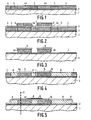
- the magnetic layer portions include also magnetic auxiliary layers 4 for obtaining a large surface area, so that during the growing operation an improved distribution of the electric current in the plating-base 2 is obtained and the growth is achieved with greater control.
- a shielding layer 5, for example a quartz layer or a photolacquer resist layer is applied on this intermediate product, portions of these layers functioning as an electrical insulation of the flux conductors 4a and 4b in a later stage of the method.
- Photolacquer resist layers 6 which function as a barrier during structuring of the composite layer are applied on the assembly of magnetic layer portions 4, 4a and 4b, photolacquer resist walls 3 and the shielding layer 5.
- Fig. 2 shows an intermediate product previous to structuring
- Fig. 3 shows the result after structuring. This structuring may for example be carried out by means of a wet chemical etching process.
- the photolacquer resist walls 3, the magnetic auxiliary layers 4 and the shielding layer 5 are partly removed.
- the shielding layer 5 must remain on the flux conductors 4a and 4b, to prevent unwanted layers from being formed during a subsequent electroplating operation on the flux conductors in the further course of the method.
- a planarized structure remains, as is shown in Fig. 5.
- An electrically insulating layer 9 and a magneto-resistance element 10 are deposited on this structure one after the other.
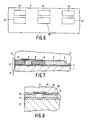
- the broken line 11 in the drawing indicates the location of the head face to be formed.
- This head face 14, see Fig. 7, is obtained after grinding of the intermediate product shown in Fig. 5.
- a filler layer 12 for example of SiO 2 , is deposited on the magnetic head structure.
- Fig. 7 shows the magnetic head obtained by means of the method described in the foregoing, the head face 14 cooperating with a schematically shown magnetic information carrier 13 which is movable in the directions indicated by the double arrow A.
- Fig. 8 shows another embodiment of a magnetic head according to a second method, which slightly deviates from the method described in the foregoing.
- this second method only the flux conductors 20 and 21 are grown by electroplating.
- a plating layer 23 is deposited on a magnetic carrier 22.
- the second magnetically insulating layer and the electrically insulating layer are formed together by an insulating layer 24 which is both mechanically and electrically insulating and is made of, for example, SiO 2 .
- This planarized insulating layer 24 is deposited for example by sputtering or CVD (chemical vapour deposition), whereafter the superfluous material is removed by etching.
- a magneto-resistance element 25, a further insulating layer 26 and a filler layer 27 are arranged one after the other on this insulating layer 24.
Landscapes
- Engineering & Computer Science (AREA)
- Manufacturing & Machinery (AREA)
- Magnetic Heads (AREA)
Applications Claiming Priority (2)
| Application Number | Priority Date | Filing Date | Title |
|---|---|---|---|
| NL9000546 | 1990-03-09 | ||
| NL9000546A NL9000546A (nl) | 1990-03-09 | 1990-03-09 | Werkwijze voor het vervaardigen van een dunnefilm magneetkop alsmede een dunnefilm magneetkop vervaardigbaar volgens de werkwijze. |
Publications (2)
| Publication Number | Publication Date |
|---|---|
| EP0445883A1 EP0445883A1 (en) | 1991-09-11 |
| EP0445883B1 true EP0445883B1 (en) | 1996-08-28 |
Family
ID=19856721
Family Applications (1)
| Application Number | Title | Priority Date | Filing Date |
|---|---|---|---|
| EP91200453A Expired - Lifetime EP0445883B1 (en) | 1990-03-09 | 1991-03-04 | Method of producing a thin-film magnetic head as well as a thin-film magnetic head producible by means of the method |
Country Status (6)
| Country | Link |
|---|---|
| US (2) | US5284572A (ko) |
| EP (1) | EP0445883B1 (ko) |
| JP (1) | JPH04216310A (ko) |
| KR (1) | KR100247877B1 (ko) |
| DE (1) | DE69121604T2 (ko) |
| NL (1) | NL9000546A (ko) |
Families Citing this family (7)
| Publication number | Priority date | Publication date | Assignee | Title |
|---|---|---|---|---|
| SG44041A1 (en) * | 1993-03-22 | 1997-11-14 | Koninkl Philips Electronics Nv | Method of manufacturing a thin-film magnetic head and magnetic head obtainable by means of said method |
| BE1007992A3 (nl) * | 1993-12-17 | 1995-12-05 | Philips Electronics Nv | Werkwijze voor het vervaardigen van een dunnefilmmagneetkop en magneetkop vervaardigd volgens de werkwijze. |
| EP0760999A1 (en) * | 1995-03-24 | 1997-03-12 | Koninklijke Philips Electronics N.V. | System comprising a magnetic head, a measuring device and a current device |
| US5982177A (en) * | 1997-08-08 | 1999-11-09 | Florida State University | Magnetoresistive sensor magnetically biased in a region spaced from a sensing region |
| WO2000017863A1 (en) * | 1998-09-24 | 2000-03-30 | Materials Innovation, Inc. | Magnetoresistive devices, giant magnetoresistive devices and methods for making same |
| US6329687B1 (en) * | 2000-01-27 | 2001-12-11 | Advanced Micro Devices, Inc. | Two bit flash cell with two floating gate regions |
| US7704614B2 (en) * | 2006-10-20 | 2010-04-27 | Seagate Technology Llc | Process for fabricating patterned magnetic recording media |
Family Cites Families (8)
| Publication number | Priority date | Publication date | Assignee | Title |
|---|---|---|---|---|
| US3921217A (en) * | 1971-12-27 | 1975-11-18 | Ibm | Three-legged magnetic recording head using a magnetorestive element |
| NL7709481A (nl) * | 1977-08-29 | 1979-03-02 | Philips Nv | Werkwijze voor het vervaardigen van een dunne film magneetkop en dunne film magneetkop ver- vaardigd met behulp van de werkwijze. |
| US4436593A (en) * | 1981-07-13 | 1984-03-13 | Memorex Corporation | Self-aligned pole tips |
| JPS5823316A (ja) * | 1981-08-04 | 1983-02-12 | Matsushita Electric Ind Co Ltd | 薄膜磁気ヘツドの製造方法 |
| JPH07105006B2 (ja) * | 1985-11-05 | 1995-11-13 | ソニー株式会社 | 磁気抵抗効果型磁気ヘツド |
| DE3644388A1 (de) * | 1985-12-27 | 1987-07-02 | Sharp Kk | Duennfilm-joch-magnetkopf |
| NL8701663A (nl) * | 1987-07-15 | 1989-02-01 | Philips Nv | Dunne film magneetkop met een magnetoweerstandselement. |
| KR940004989B1 (ko) * | 1989-08-04 | 1994-06-09 | 마쯔시다덴기산교 가부시기가이샤 | 박막자기헤드 |
-
1990
- 1990-03-09 NL NL9000546A patent/NL9000546A/nl not_active Application Discontinuation
-
1991
- 1991-03-04 DE DE69121604T patent/DE69121604T2/de not_active Expired - Fee Related
- 1991-03-04 US US07/664,164 patent/US5284572A/en not_active Expired - Fee Related
- 1991-03-04 EP EP91200453A patent/EP0445883B1/en not_active Expired - Lifetime
- 1991-03-06 KR KR1019910003579A patent/KR100247877B1/ko not_active Expired - Fee Related
- 1991-03-07 JP JP3065295A patent/JPH04216310A/ja active Pending
-
1995
- 1995-03-22 US US08/408,451 patent/US5473490A/en not_active Expired - Fee Related
Non-Patent Citations (1)
| Title |
|---|
| PATENT ABSTRACTS OF JAPAN, vol. 12, no. 123 (P-690) [2970], April 16, 1988 from JP-A-62-246115 * |
Also Published As
| Publication number | Publication date |
|---|---|
| JPH04216310A (ja) | 1992-08-06 |
| EP0445883A1 (en) | 1991-09-11 |
| DE69121604D1 (de) | 1996-10-02 |
| NL9000546A (nl) | 1991-10-01 |
| KR910017367A (ko) | 1991-11-05 |
| US5284572A (en) | 1994-02-08 |
| US5473490A (en) | 1995-12-05 |
| KR100247877B1 (ko) | 2000-03-15 |
| DE69121604T2 (de) | 1997-03-06 |
Similar Documents
| Publication | Publication Date | Title |
|---|---|---|
| US4684438A (en) | Process for producing a coil for a magnetic recording head | |
| US5189580A (en) | Ultra small track width thin film magnetic transducer | |
| US5016342A (en) | Method of manufacturing ultra small track width thin film transducers | |
| JPH0644332B2 (ja) | 垂直記録用の録再磁気ヘッドの製造方法 | |
| US5901431A (en) | Method of fabricating a thin film inductive head having a second pole piece having a mushroom yoke portion | |
| US7086138B2 (en) | Method of forming a feature having a high aspect ratio | |
| US4614563A (en) | Process for producing multilayer conductor structure | |
| GB2083230A (en) | Method of manufacturing a thin film magnetic field sensor | |
| US5123156A (en) | Method for the production of a read-write magnetic head | |
| JPH11259812A (ja) | 薄膜磁気ヘッドおよびその製造方法 | |
| EP0445883B1 (en) | Method of producing a thin-film magnetic head as well as a thin-film magnetic head producible by means of the method | |
| KR100420590B1 (ko) | 집적된코일을갖는수직자기헤드및그제조방법 | |
| US5815909A (en) | Method of making a thin film magnetic head including protected via connections through an electrically insulative substrate | |
| KR100666020B1 (ko) | 자기헤드에 대한 시드층 제거를 위한 방법 | |
| KR100249975B1 (ko) | 자기 기록 재생 헤드 및 그 제조 방법 | |
| US6167611B1 (en) | Process for producing a vertical magnetic head | |
| US5034089A (en) | Method of manufacturing a multi-turn multi-track composite recording head | |
| US4829659A (en) | Process for the production of a magnetic hea making it possible to simplify the production of electrical connections | |
| JPS58108017A (ja) | 薄膜磁気ヘツド | |
| US4729050A (en) | Thin-film vertical magnetization transducer head | |
| JP2535819B2 (ja) | 薄膜磁気ヘッドの製造方法 | |
| JPH087222A (ja) | 薄膜磁気ヘッド及びその製造方法 | |
| KR0171141B1 (ko) | 박막 자기 헤드 제작 방법 | |
| JP2565188B2 (ja) | 薄膜磁気ヘツドの製法 | |
| JPH06124416A (ja) | 薄膜磁気ヘッドの製造方法 |
Legal Events
| Date | Code | Title | Description |
|---|---|---|---|
| PUAI | Public reference made under article 153(3) epc to a published international application that has entered the european phase |
Free format text: ORIGINAL CODE: 0009012 |
|
| AK | Designated contracting states |
Kind code of ref document: A1 Designated state(s): DE FR GB IT |
|
| 17P | Request for examination filed |
Effective date: 19920311 |
|
| 17Q | First examination report despatched |
Effective date: 19940907 |
|
| GRAH | Despatch of communication of intention to grant a patent |
Free format text: ORIGINAL CODE: EPIDOS IGRA |
|
| GRAH | Despatch of communication of intention to grant a patent |
Free format text: ORIGINAL CODE: EPIDOS IGRA |
|
| GRAA | (expected) grant |
Free format text: ORIGINAL CODE: 0009210 |
|
| AK | Designated contracting states |
Kind code of ref document: B1 Designated state(s): DE FR GB IT |
|
| REF | Corresponds to: |
Ref document number: 69121604 Country of ref document: DE Date of ref document: 19961002 |
|
| ITF | It: translation for a ep patent filed | ||
| ET | Fr: translation filed | ||
| PLBE | No opposition filed within time limit |
Free format text: ORIGINAL CODE: 0009261 |
|
| STAA | Information on the status of an ep patent application or granted ep patent |
Free format text: STATUS: NO OPPOSITION FILED WITHIN TIME LIMIT |
|
| 26N | No opposition filed | ||
| REG | Reference to a national code |
Ref country code: FR Ref legal event code: CD |
|
| PGFP | Annual fee paid to national office [announced via postgrant information from national office to epo] |
Ref country code: FR Payment date: 20010326 Year of fee payment: 11 |
|
| PGFP | Annual fee paid to national office [announced via postgrant information from national office to epo] |
Ref country code: GB Payment date: 20010330 Year of fee payment: 11 |
|
| PGFP | Annual fee paid to national office [announced via postgrant information from national office to epo] |
Ref country code: DE Payment date: 20010516 Year of fee payment: 11 |
|
| REG | Reference to a national code |
Ref country code: GB Ref legal event code: IF02 |
|
| PG25 | Lapsed in a contracting state [announced via postgrant information from national office to epo] |
Ref country code: GB Free format text: LAPSE BECAUSE OF NON-PAYMENT OF DUE FEES Effective date: 20020304 |
|
| PG25 | Lapsed in a contracting state [announced via postgrant information from national office to epo] |
Ref country code: DE Free format text: LAPSE BECAUSE OF NON-PAYMENT OF DUE FEES Effective date: 20021001 |
|
| GBPC | Gb: european patent ceased through non-payment of renewal fee |
Effective date: 20020304 |
|
| PG25 | Lapsed in a contracting state [announced via postgrant information from national office to epo] |
Ref country code: FR Free format text: LAPSE BECAUSE OF NON-PAYMENT OF DUE FEES Effective date: 20021129 |
|
| REG | Reference to a national code |
Ref country code: FR Ref legal event code: ST |
|
| PG25 | Lapsed in a contracting state [announced via postgrant information from national office to epo] |
Ref country code: IT Free format text: LAPSE BECAUSE OF NON-PAYMENT OF DUE FEES Effective date: 20050304 |