EP0446050B1 - Dispositif de commutation de signaux d'émission/réception - Google Patents
Dispositif de commutation de signaux d'émission/réception Download PDFInfo
- Publication number
- EP0446050B1 EP0446050B1 EP91301903A EP91301903A EP0446050B1 EP 0446050 B1 EP0446050 B1 EP 0446050B1 EP 91301903 A EP91301903 A EP 91301903A EP 91301903 A EP91301903 A EP 91301903A EP 0446050 B1 EP0446050 B1 EP 0446050B1
- Authority
- EP
- European Patent Office
- Prior art keywords
- transmission
- signal
- switching
- reception
- line
- Prior art date
- Legal status (The legal status is an assumption and is not a legal conclusion. Google has not performed a legal analysis and makes no representation as to the accuracy of the status listed.)
- Expired - Lifetime
Links
Images


Classifications
-
- H—ELECTRICITY
- H01—ELECTRIC ELEMENTS
- H01Q—ANTENNAS, i.e. RADIO AERIALS
- H01Q1/00—Details of, or arrangements associated with, antennas
- H01Q1/52—Means for reducing coupling between antennas; Means for reducing coupling between an antenna and another structure
- H01Q1/521—Means for reducing coupling between antennas; Means for reducing coupling between an antenna and another structure reducing the coupling between adjacent antennas
- H01Q1/525—Means for reducing coupling between antennas; Means for reducing coupling between an antenna and another structure reducing the coupling between adjacent antennas between emitting and receiving antennas
-
- H—ELECTRICITY
- H04—ELECTRIC COMMUNICATION TECHNIQUE
- H04B—TRANSMISSION
- H04B1/00—Details of transmission systems, not covered by a single one of groups H04B3/00 - H04B13/00; Details of transmission systems not characterised by the medium used for transmission
- H04B1/38—Transceivers, i.e. devices in which transmitter and receiver form a structural unit and in which at least one part is used for functions of transmitting and receiving
- H04B1/40—Circuits
- H04B1/44—Transmit/receive switching
- H04B1/48—Transmit/receive switching in circuits for connecting transmitter and receiver to a common transmission path, e.g. by energy of transmitter
Definitions
- the present invention generally relates to switching apparatus and, more particularly, is directed to a signal transmission/reception switching apparatus.
- a telephone communication is carried out in a so-called bidirectional fashion so that the transmission of its own audio signal and the reception of an audio signal from the other party are constantly performed simultaneously.
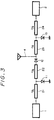
- a transmitting circuit 1 and a receiving circuit 2 are connected to an antenna 4 through a separating circuit 3 which is what might be called a duplexer.
- the duplexer 3 is generally composed of a bandpass filter whose pass band is the frequency of a transmitting signal and a bandpass filter whose pass band is the frequency of a receiving signal. This method utilizing the duplexer 3 is effective when the transmitting frequency and the receiving frequency are considerably distant from each other.
- the transmitting frequency and the receiving frequency are 800 to 900 MHz, respectively, and a difference between the transmitting frequency and the receiving frequency is 45 MHz at any one of the channels. Accordingly, if the transmitting circuit 1 and the receiving circuit 2 are connected through the duplexer 3 to the antenna 4, cut-off frequency characteristics of the bandpass filters of the duplexer 3 must be made steep because the transmitting frequency and the receiving frequency are both high and they are close to each other. However, the bandpass filters having such steep cut-off frequency characteristics cannot be produced without difficulty from a technological standpoint, which increases the loss of signals and the increase of size, weight and cost of the digital mobile telephone.
- the transmitting circuit 1 and the receiving circuit 2 are switched by a change-over circuit (switching circuit) 5 and then can be connected to the antenna 4.
- the switching circuit 5 is generally constructed as, for example, shown in Fig. 3.
- reference numerals 11, 12 and 13 denote PIN (positive-intrinsic-negative) diodes, and 21, 22, 23 and 24 1/4 wavelength coaxial lines, respectively.
- the diode 11 Upon transmission, the diode 11 is turned OFF and the diodes 12, 13 are turned ON, whereas upon reception, the diode 11 is turned ON and the diodes 12, 13 are turned OFF.
- the diodes 11, 12 and 13 have a relatively large resistance value so that Q is lowered, thus making it impossible to obtain a high isolation.
- the transmission signal is passed through the diode 12 having the large resistance value, a transmission loss occurs in the transmission signal, thereby an antenna output is lowered. Furthermore, since isolation is low, the transmission signal also leaks to the receiving circuit 2 side, thereby further increasing transmission loss.
- the transmitting circuit 1 in order to obtain a proper antenna output, the transmitting circuit 1 must transmit a larger transmission output, which is disadvantageous for a power supply source battery. Furthermore, since the transmission loss in the diode 12 is large, the diode 12 must have large withstand voltage, which increases a manufacturing cost of the switching circuit 5.
- JP-A-60-174,534 discloses an apparatus in accordance with the preamble of claim 1 but in which variable reactances are used as the switching elements.
- a signal transmission/reception switching apparatus in which a transmission signal and a reception signal are selectively switched to access an antenna, comprising:
- a signal transmission/reception switching apparatus can have higher isolation and transmission loss can be prevented from being produced in a transmission signal. Also reception sensitivity can be prevented from being lowered and the signal transmission reception switching apparatus can be made inexpensive.
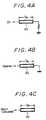
- a length (effective length) of a coaxial line 30 is selected to be 1/4 of a wavelength ⁇ of a signal, and if an impedance Zo equal to a characteristic impedance of this coaxial line 30 is connected to an output end of the coaxial line 30 as shown in Fig. 4A, an impedance becomes value Zo when seen from the input end of the coaxial line 30.
- impedance becomes zero (short) when seen from the input end of the coaxial line 30.
- the transmitting frequency and the receiving frequency are high and a difference therebetween is as sufficiently small as about 5 % as compared with the transmitting frequency and the receiving frequency.
- the present invention is intended to provide the signal transmission reception switching apparatus in which the coaxial line itself is utilized as a switch for switching the connection to an antenna.
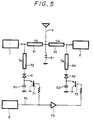
- an output terminal of a transmitting circuit 1 is connected to an antenna 4 through a coaxial line 31, and a coaxial line 32, a switching diode 41 and a bypass capacitor 51 are connected in series between the output terminal of the transmitting circuit 1 and the ground.
- a coaxial line 33 is connected between the antenna 4 and the input terminal of a receiving circuit 2, and a coaxial line 34, a switching diode 42 and a bypass capacitor 52 are connected in series between the input terminal of the receiving circuit 2 and the ground.
- a high frequency choke coil 61 for a DC line is connected between the antenna 4 and the ground, and also an emitter-collector path of a switching transistor 71 is connected between a junction P1 of the switching diode 41 to the bypass capacitor 51 and a power supply source line. Further, an emitter-collector path of a switching transistor 72 is connected between a junction P2 of the switching diode 42 to the bypass capacitor 52 and the power supply source line.
- Characteristic impedances of the respective coaxial lines 31 to 34 are made equal to an output impedance of the transmitting circuit 1, an impedance of the antenna 4 and an input impedance of the receiving circuit 2, and also a length (effective length) of each of the coaxial lines 31 to 34 is selected to be 1/4 of an average wavelength ⁇ of transmission and reception wavelengths.
- the switching diodes 41 and 42 are formed of PIN diodes, respectively.
- a control circuit 6 derives a switching pulse Ps which goes high level “1" during a transmission period of the TDMA system and which goes low level "0" during a reception period thereof.
- This switching pulse Ps is supplied to the base of the transistor 71 and is also supplied through an inverter 73 to the base of the transistor 72.
- the equivalent circuit of Fig. 6A can be rewritten as an equivalent circuit shown in Fig. 6B on the basis of the fundamental principle as earlier noted with reference to Figs. 4A to 4C, and further, the equivalent circuit of Fig. 6A can be rewritten as an equivalent circuit shown in Fig. 6C.
- the output terminal of the transmitting circuit 1 is connected to the antenna 4 and the input terminal of the receiving circuit 2 is grounded, whereby the transmission is performed.
- the output terminal of the transmitting circuit 1 is grounded and the antenna 4 is connected to the input terminal of the receiving circuit 2.
- the transmitting circuit 1 and the receiving circuit 2 are selectively connected to the antenna 4.
- the coaxial lines 31 to 34 are given switching functions to thereby switch the signal transmission and reception so that Q can be prevented from being lowered. Therefore, the closer the transmitting and receiving frequencies become, which provides a disadvantage in the general switching apparatus, the higher the isolation can be made.
- the transmission signal does not pass through the switching diodes 41 to 42 having large resistance values, a transmission loss can be prevented from being produced in the transmission signal and hence the antenna output can be prevented from being lowered. Furthermore, since the isolation is high, the transmission signal can be prevented from being leaked to the receiving circuit 2 side and a transmission loss can be avoided also.
- the transmission output of the transmitting circuit 1 need not be increased excessively in order to obtain a proper antenna output, which is advantageous for the power supply source battery. Further, since the transmission signal and the reception signal are prevented from passing through the switching diodes 41 and 42, the switching diodes 41 and 42 might be such ones having small power withstand property, which can reduce the manufacturing cost.
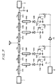
- Fig. 7 shows a second embodiment of the signal transmission reception switching apparatus according to the present invention, in which the switching circuits are constructed in a multiplestage fashion.
- coaxial lines 31A to 34B, switching diodes 41A to 42B, bypass capacitors 51A to 52B and switching transistors 71A to 72B are connected in a multiple-stage fashion similarly to the coaxial lines 31 to 34, the switching diodes 41 and 42, the bypass capacitors 51 and 52 and the switching transistors 71 and 72.
- the length of each of the coaxial lines 31A, 31C, 33A and 33C is selected to be 1/4 of the average wavelength ⁇ of the transmission and reception wavelengths
- the length of each of the coaxial lines 31B and 33B is selected to be 1/2 of the average wavelength ⁇ of the transmission and reception wavelengths.
- the length of each of the coaxial lines 32A, 32B, 34A and 34B is also selected to be ⁇ /4.
- each of the coaxial lines 31B and 33B is selected to be 1/2 of the average wavelength ⁇ of the transmission and reception wavelengths as described above, impedance (opened or short circuited) of each of the output terminal is directly reflected on the input terminal thereof, whereby the transmitting circuit 1 and the receiving circuit 2 are selectively connected to the antenna 4 similarly as described above.
- the switching circuit since the switching circuit is constructed in a multiple-stage fashion, isolation can be made higher.
- the transmission signal and the reception signal are only transmitted through the coaxial lines 31A to 31C and 33A to 33C, respectively, loss can be avoided substantially.
- the coaxial lines 31B and 33B may be replaced with PIN diodes.
- the coaxial lines 31 to 34 are given switching functions to thereby switch the signal transmission and reception so that Q can be prevented from being lowered. Therefore, the closer the transmitting and receiving frequencies become, which provides a disadvantage in the general switching apparatus, the higher the isolation can be made.
- the transmission signal is not passed through the switching diodes 41 to 42 having large resistance values, a transmission loss can be prevented from being produced in the transmission signal and the antenna output can be prevented from being lowered. Furthermore, since the isolation is high, the transmission signal can be prevented from being leaked to the receiving circuit 2 side and a transmission loss can be avoided also.
- the transmission output of the transmitting circuit 1 need not be increased excessively in order to obtain a proper antenna output, which is advantageous for the power supply source battery. Further, since the transmission signal and the reception signal are prevented from passing through the switching diodes 41 and 42, the switching diodes 41 and 42 might be such ones having small power withstand property, which can reduce the manufacturing cost.
Landscapes
- Engineering & Computer Science (AREA)
- Computer Networks & Wireless Communication (AREA)
- Signal Processing (AREA)
- Transceivers (AREA)
- Waveguide Switches, Polarizers, And Phase Shifters (AREA)
Claims (8)
- Dispositif de commutation de signaux d'émission/réception dans lequel un signal d'émission et un signal de réception sont sélectivement commutés pour accéder à une antenne, comprenant :(a) une première ligne de transmission (31) raccordée entre une première borne (1) à laquelle ledit signal d'émission est appliqué et une borne d'antenne ;(b) une seconde ligne de transmission (32) et un premier élément de commutation (41, 51, 71) raccordés en série entre ladite borne à laquelle ledit signal d'émission est appliqué et la masse ;(c) une troisième ligne de transmission (33) raccordée entre ladite borne d'antenne et une seconde borne (2) à laquelle ledit signal de réception est appliqué ; et(d) une quatrième ligne de transmission (34) et un second élément de commutation (42, 52, 72) raccordés en série entre ladite borne à laquelle ledit signal de réception est appliqué et la masse, la longueur de chacune desdites première à la quatrième lignes de transmission (31 à 34) étant sélectionnée pour être de 1/4 de la longueur d'onde moyenne λ desdits signaux d'émission et de réception, dans lequel lorsque ledit signal d'émission est émis, ledit premier élément de commutation (41, 51, 71) est conducteur et ledit second élément de commutation (42, 52, 72) est bloqué, alors que lorsque ledit signal de réception est reçu, ledit premier élément de commutation (41, 51, 71) est bloqué et ledit second élément de commutation (42, 52, 72) est conducteur, caractérisé en ce que :chacun desdits premier et second éléments de commutation comprend une diode de commutation (41, 42) et un condensateur de dérivation (51, 52) raccordés en série entre la ligne de transmission respective et la masse et un transistor de commutation (71, 72) dont le chemin émetteur-collecteur est raccordé en parallèle audit condensateur de dérivation.
- Dispositif de commutation de signaux d'émission/réception selon la revendication 1, dans lequel lesdites première à la quatrième lignes de transmission (31 à 34) sont des lignes coaxiales.
- Dispositif de commutation de signaux d'émission/réception selon la revendication 1 ou 2, dans lequel lesdites diodes de commutation (41, 42) sont des diodes PIN.
- Dispositif de commutation de signaux d'émission/réception selon la revendication 1, 2 ou 3, dans lequel lesdites première à quatrième lignes de transmission (31 à 34) et lesdits premier et second éléments de commutation (41, 51, 71 ; 42, 52, 72) sont disposés d'une manière à étages multiples.
- Dispositif de commutation de signaux d'émission/réception selon la revendication 1, 2, 3 ou 4, dans lequel ladite première ligne de transmission (31) est une première ligne coaxiale (31C), et dans lequel la seconde (31B) et la troisième (31A) lignes coaxiales sont raccordées en série entre ladite première borne (1) et ladite première ligne coaxiale (31C), ladite troisième ligne de transmission (33) est une quatrième ligne coaxiale (33A), et dans lequel les cinquième (33B) et sixième (33C) lignes coaxiales sont raccordées en série entre ladite seconde borne (2) et ladite quatrième ligne coaxiale (33A).
- Dispositif de commutation de signaux d'émission/réception selon la revendication 5, dans lequel la longueur de chacune desdites première (31C) et troisième (31A) lignes coaxiales est sélectionnée pour être de λ/4, alors que la longueur de ladite seconde ligne coaxiale (31B) est sélectionnée pour être de λ/2.
- Dispositif de commutation de signaux d'émission/réception selon la revendication 7, dans lequel la longueur de chacune desdites quatrième (33A) et sixième (33C) lignes coaxiales est sélectionnée pour être de λ/4, alors que la longueur de ladite cinquième ligne coaxiale (33B) est sélectionnée pour être de λ/2.
- Téléphone comprenant un dispositif de commutation de signaux d'émission/réception selon l'une quelconque des revendications précédentes.
Applications Claiming Priority (2)
| Application Number | Priority Date | Filing Date | Title |
|---|---|---|---|
| JP57676/90 | 1990-03-08 | ||
| JP2057676A JP2830319B2 (ja) | 1990-03-08 | 1990-03-08 | 送受信切り換え装置 |
Publications (3)
| Publication Number | Publication Date |
|---|---|
| EP0446050A2 EP0446050A2 (fr) | 1991-09-11 |
| EP0446050A3 EP0446050A3 (en) | 1992-09-02 |
| EP0446050B1 true EP0446050B1 (fr) | 1996-08-14 |
Family
ID=13062526
Family Applications (1)
| Application Number | Title | Priority Date | Filing Date |
|---|---|---|---|
| EP91301903A Expired - Lifetime EP0446050B1 (fr) | 1990-03-08 | 1991-03-07 | Dispositif de commutation de signaux d'émission/réception |
Country Status (4)
| Country | Link |
|---|---|
| US (1) | US5193218A (fr) |
| EP (1) | EP0446050B1 (fr) |
| JP (1) | JP2830319B2 (fr) |
| DE (1) | DE69121263T2 (fr) |
Cited By (2)
| Publication number | Priority date | Publication date | Assignee | Title |
|---|---|---|---|---|
| DE102004033268A1 (de) * | 2004-07-09 | 2006-02-02 | Atmel Germany Gmbh | Hochfrequenzschaltung |
| DE102008013386A1 (de) * | 2008-03-10 | 2009-09-24 | Andrew Wireless Systems Gmbh | Hochfrequenz-Kurzschluss-Schalter sowie Schaltungseinheit |
Families Citing this family (73)
| Publication number | Priority date | Publication date | Assignee | Title |
|---|---|---|---|---|
| FI90926C (fi) * | 1992-05-14 | 1994-04-11 | Lk Products Oy | Vaihtokytkimenä toimiva suurtaajuussuodatin |
| DE4222190A1 (de) * | 1992-07-07 | 1994-01-13 | Philips Patentverwaltung | Funkgerät mit einer Antennenumschaltvorrichtung |
| US5296762A (en) * | 1992-11-04 | 1994-03-22 | Rockwell International Corporation | Bidirectional microwave amplifier apparatus |
| US5507011A (en) * | 1992-12-22 | 1996-04-09 | Murata Manufacturing Co., Ltd. | High-frequency switch including strip line and two switching diodes |
| JP2874496B2 (ja) * | 1992-12-26 | 1999-03-24 | 株式会社村田製作所 | 高周波スイッチ |
| JP3243892B2 (ja) * | 1993-05-21 | 2002-01-07 | ソニー株式会社 | 信号切り替え用スイッチ |
| JPH077449A (ja) * | 1993-06-17 | 1995-01-10 | Oki Electric Ind Co Ltd | アンテナ切り替えスイッチ |
| US5594394A (en) * | 1993-08-31 | 1997-01-14 | Matsushita Electric Industrial Co., Ltd. | Antenna diversity switching device with switching circuits between the receiver terminal and each antenna |
| FI97086C (fi) * | 1994-02-09 | 1996-10-10 | Lk Products Oy | Järjestely lähetyksen ja vastaanoton erottamiseksi |
| JPH07263901A (ja) * | 1994-03-24 | 1995-10-13 | Murata Mfg Co Ltd | 高周波部品 |
| US5440283A (en) * | 1994-06-14 | 1995-08-08 | Sierra Microwave Technology | Inverted pin diode switch apparatus |
| JPH0851381A (ja) * | 1994-08-04 | 1996-02-20 | Uniden Corp | 集積化が可能な高周波用ポート選択回路 |
| JP3169775B2 (ja) * | 1994-08-29 | 2001-05-28 | 株式会社日立製作所 | 半導体回路、スイッチ及びそれを用いた通信機 |
| US5541980A (en) * | 1994-10-27 | 1996-07-30 | Cobra Electronics Corporation | Cordless telephone/radio-monitoring system |
| JPH08237165A (ja) * | 1995-02-24 | 1996-09-13 | Murata Mfg Co Ltd | アンテナ共用器 |
| FI101117B (fi) * | 1995-09-22 | 1998-04-15 | Nokia Mobile Phones Ltd | Aikajakoisessa radiopuhelinjärjestelmässä toimiva radiopuhelin |
| DE19610760A1 (de) * | 1996-03-19 | 1997-09-25 | Telefunken Microelectron | Sende-Empfangs-Umschalter mit Halbleitern |
| JPH09331206A (ja) * | 1996-06-12 | 1997-12-22 | Saitama Nippon Denki Kk | Tdma方式用携帯電話機のアンテナ整合部 |
| US6249670B1 (en) * | 1997-01-13 | 2001-06-19 | Telefonaktiebolaget Lm Ericsson (Publ) | Signal combining device and method for radio communication |
| DE19704151C1 (de) * | 1997-02-04 | 1998-08-27 | Siemens Ag | Sende-Empfangs-Umschalteanordnung |
| US5909641A (en) * | 1997-02-24 | 1999-06-01 | At&T Wireless Services Inc. | Transmit/receive switch |
| DE69834679T2 (de) * | 1997-03-12 | 2006-09-21 | Matsushita Electric Industrial Co., Ltd., Kadoma | Antennenweiche |
| US5815804A (en) * | 1997-04-17 | 1998-09-29 | Motorola | Dual-band filter network |
| JPH11122139A (ja) * | 1997-10-17 | 1999-04-30 | Murata Mfg Co Ltd | アンテナ共用器 |
| US6009314A (en) * | 1997-11-17 | 1999-12-28 | Telefonaktiebolaget L/M Ericsson | Monolithic high frequency antenna switch |
| JPH11312907A (ja) * | 1997-12-18 | 1999-11-09 | Matsushita Electric Ind Co Ltd | 整合回路チップ、整合回路付きフィルタ、共用器、及び移動体通信機器 |
| DE19757142A1 (de) * | 1997-12-20 | 1999-07-08 | Philips Patentverwaltung | Mobilfunkgerät |
| DE19842706A1 (de) * | 1998-09-17 | 2000-03-23 | Siemens Ag | Mehrband-Antennenschalter |
| JP2000134130A (ja) * | 1998-10-22 | 2000-05-12 | Matsushita Electric Ind Co Ltd | 送受切替スイッチ |
| WO2000041326A1 (fr) * | 1999-01-07 | 2000-07-13 | Motorola Inc. | Commutateur h.f. utilisant une seule section d'isolation quart d'onde et son procede de formation |
| DK1039652T3 (da) * | 1999-03-19 | 2007-07-02 | Asulab Sa | Antennearrangement |
| JP4207328B2 (ja) | 1999-09-14 | 2009-01-14 | ソニー株式会社 | アンテナ切り換え回路及びそれを用いた通信装置 |
| DE19948964C2 (de) * | 1999-10-11 | 2001-10-04 | Texas Instruments Deutschland | Schaltungsanordnung zum Herstellen einer unidirektionalen Verbindung zwischen Sende- und/oder Empfangsgeräten und einer Antenne |
| US6552626B2 (en) * | 2000-01-12 | 2003-04-22 | Raytheon Company | High power pin diode switch |
| EP1124334A1 (fr) * | 2000-02-10 | 2001-08-16 | Siemens Aktiengesellschaft | Emetteur-récepteur pour l'émission et la réception de signaux radio |
| US6721544B1 (en) * | 2000-11-09 | 2004-04-13 | Intel Corporation | Duplexer structure for coupling a transmitter and a receiver to a common antenna |
| FI20002902A7 (fi) * | 2000-12-29 | 2002-06-30 | Nokia Corp | Viestintälaite ja menetelmä lähettimen ja vastaanottimen kytkemiseksi |
| DE60116676T2 (de) | 2001-02-27 | 2006-10-19 | Telefonaktiebolaget Lm Ericsson (Publ) | Mehrband-Transformationsstufe für eine Mehrband-HF-Umschaltvorrichtung |
| US20030022631A1 (en) * | 2001-07-13 | 2003-01-30 | Rhodes Robert Andrew | Multi-mode bidirectional communications device including a diplexer having a switchable notch filter |
| FR2828584A1 (fr) * | 2001-08-10 | 2003-02-14 | Thomson Licensing Sa | Dispositif pour la reception et/ou l'emission de signaux a diversite de rayonnement |
| JP2003087002A (ja) * | 2001-09-14 | 2003-03-20 | Matsushita Electric Ind Co Ltd | 高周波スイッチ |
| ATE451627T1 (de) | 2002-03-22 | 2009-12-15 | Ericsson Telefon Ab L M | Sende-empfangs-schalter mit hochleistungsschutz |
| US7515894B2 (en) * | 2002-03-26 | 2009-04-07 | Kyocera Wireless Corp. | System and method for providing a multiband antenna |
| US6987950B2 (en) * | 2002-07-25 | 2006-01-17 | Qualcomm, Incorporated | Radio with duplexer bypass capability |
| DE10305302A1 (de) * | 2003-02-10 | 2004-08-19 | Valeo Schalter Und Sensoren Gmbh | Hochfrequenz-Schaltvorrichtung |
| JP2005268878A (ja) * | 2004-03-16 | 2005-09-29 | Matsushita Electric Ind Co Ltd | アンテナ共用器 |
| US8134799B1 (en) | 2004-04-06 | 2012-03-13 | Oracle America, Inc. | Gripper assembly for data storage system |
| JP2005311447A (ja) * | 2004-04-16 | 2005-11-04 | Toshiba Corp | スイッチ回路 |
| US7274913B2 (en) * | 2004-10-15 | 2007-09-25 | Broadcom Corporation | Transceiver system and method of using same |
| JP3936949B2 (ja) * | 2004-10-25 | 2007-06-27 | 株式会社日立国際電気 | 高周波スイッチ回路装置 |
| JP4642570B2 (ja) * | 2005-07-06 | 2011-03-02 | 日本電信電話株式会社 | 高周波スイッチ回路、無線機器及び信号経路切り替え器 |
| JP4718308B2 (ja) * | 2005-11-25 | 2011-07-06 | 三菱電機株式会社 | 高周波スイッチ |
| KR100841638B1 (ko) * | 2006-04-25 | 2008-06-26 | 삼성전자주식회사 | 시분할복신 무선통신시스템의 수신부 보호 장치 |
| US7498908B2 (en) * | 2006-08-04 | 2009-03-03 | Advanced Energy Industries, Inc | High-power PIN diode switch |
| US7612633B2 (en) * | 2006-11-07 | 2009-11-03 | Mitsubishi Electric Corporation | High-frequency switch |
| TWI338970B (en) * | 2007-11-02 | 2011-03-11 | Univ Nat Taiwan | Single-pole-double-throw switch integrated with bandpass filtering function |
| US8390394B2 (en) | 2007-12-19 | 2013-03-05 | Soshin Electric Co., Ltd. | High frequency switch |
| JP2009152749A (ja) * | 2007-12-19 | 2009-07-09 | Soshin Electric Co Ltd | 信号切替スイッチ |
| JP5002509B2 (ja) * | 2008-03-28 | 2012-08-15 | 双信電機株式会社 | 高周波スイッチ |
| JP5049886B2 (ja) | 2008-06-06 | 2012-10-17 | 双信電機株式会社 | 高周波スイッチ |
| JP5261119B2 (ja) | 2008-09-30 | 2013-08-14 | 双信電機株式会社 | 高周波スイッチ |
| FR2937481B1 (fr) | 2008-10-17 | 2011-03-25 | Thales Sa | Dispositif de commutation electronique pour signaux a haute frequence |
| JP5287286B2 (ja) * | 2009-01-21 | 2013-09-11 | 富士通株式会社 | バイアス回路 |
| JP2010206369A (ja) * | 2009-03-02 | 2010-09-16 | Nec Corp | 信号遮断装置及びこれを用いた無線基地局装置の試験方法 |
| US8106728B2 (en) * | 2009-04-15 | 2012-01-31 | International Business Machines Corporation | Circuit structure and design structure for an optionally switchable on-chip slow wave transmission line band-stop filter and a method of manufacture |
| US8027648B2 (en) * | 2009-04-29 | 2011-09-27 | Lockheed Martin Corporation | Radio frequency power monitor |
| US8446232B2 (en) * | 2009-06-01 | 2013-05-21 | Arizona Board Of Regents For And On Behalf Of Arizona State University | Ultra-wideband tunable filters based on multi-resolution band-selection |
| US9030252B2 (en) * | 2011-05-24 | 2015-05-12 | Imagineering, Inc. | High frequency switching device, and bias voltage outputting device |
| JP6292447B2 (ja) * | 2013-06-07 | 2018-03-14 | パナソニックIpマネジメント株式会社 | 送受信切替装置 |
| US10027366B2 (en) | 2014-04-25 | 2018-07-17 | Raytheon Company | High power radio frequency (RF) antenna switch |
| EP3460902A4 (fr) * | 2016-06-28 | 2019-06-26 | Mitsubishi Electric Corporation | Commutateur haute fréquence |
| WO2018109896A1 (fr) * | 2016-12-15 | 2018-06-21 | 三菱電機株式会社 | Commutateur haute fréquence |
| EP3703267A1 (fr) * | 2019-02-27 | 2020-09-02 | Nxp B.V. | Agencement de commutateur |
Citations (1)
| Publication number | Priority date | Publication date | Assignee | Title |
|---|---|---|---|---|
| JPS60174534A (ja) * | 1984-02-20 | 1985-09-07 | Toyo Commun Equip Co Ltd | アンテナ・スイツチ回路 |
Family Cites Families (6)
| Publication number | Priority date | Publication date | Assignee | Title |
|---|---|---|---|---|
| US3339140A (en) * | 1964-08-04 | 1967-08-29 | Nevlin C Pace | Solid-state two-way radio switching system application |
| US3327215A (en) * | 1964-09-18 | 1967-06-20 | Motorola Inc | Electronic circuit for selectively connecting a transmitter and a receiver to a single antenna |
| US3471787A (en) * | 1966-05-06 | 1969-10-07 | Gen Dynamics Corp | Duplexing system |
| US4399557A (en) * | 1981-12-15 | 1983-08-16 | Motorola Inc. | Minimum power, feedback controller, transmit/receive switch |
| US5060293A (en) * | 1989-10-20 | 1991-10-22 | Motorola, Inc. | Antenna switch for transmit-receive operation using relays and diodes |
| US5023935A (en) * | 1989-11-17 | 1991-06-11 | Nynex Corporation | Combined multi-port transmit/receive switch and filter |
-
1990
- 1990-03-08 JP JP2057676A patent/JP2830319B2/ja not_active Expired - Fee Related
-
1991
- 1991-03-04 US US07/664,214 patent/US5193218A/en not_active Expired - Fee Related
- 1991-03-07 DE DE69121263T patent/DE69121263T2/de not_active Expired - Fee Related
- 1991-03-07 EP EP91301903A patent/EP0446050B1/fr not_active Expired - Lifetime
Patent Citations (1)
| Publication number | Priority date | Publication date | Assignee | Title |
|---|---|---|---|---|
| JPS60174534A (ja) * | 1984-02-20 | 1985-09-07 | Toyo Commun Equip Co Ltd | アンテナ・スイツチ回路 |
Non-Patent Citations (1)
| Title |
|---|
| Arizona. USA. "6-19 GHz GaAs FET Transmit-Receive switch." Ayasli et al. * |
Cited By (2)
| Publication number | Priority date | Publication date | Assignee | Title |
|---|---|---|---|---|
| DE102004033268A1 (de) * | 2004-07-09 | 2006-02-02 | Atmel Germany Gmbh | Hochfrequenzschaltung |
| DE102008013386A1 (de) * | 2008-03-10 | 2009-09-24 | Andrew Wireless Systems Gmbh | Hochfrequenz-Kurzschluss-Schalter sowie Schaltungseinheit |
Also Published As
| Publication number | Publication date |
|---|---|
| JP2830319B2 (ja) | 1998-12-02 |
| DE69121263D1 (de) | 1996-09-19 |
| EP0446050A2 (fr) | 1991-09-11 |
| JPH03258126A (ja) | 1991-11-18 |
| US5193218A (en) | 1993-03-09 |
| DE69121263T2 (de) | 1997-02-06 |
| EP0446050A3 (en) | 1992-09-02 |
Similar Documents
| Publication | Publication Date | Title |
|---|---|---|
| EP0446050B1 (fr) | Dispositif de commutation de signaux d'émission/réception | |
| US5634200A (en) | Antenna duplexer and transmitting/receiving apparatus using the same | |
| US7339445B2 (en) | BAW duplexer without phase shifter | |
| EP1080540B1 (fr) | Adaptation perfectionnee d'un amplificateur de puissance dans un telephone mobile a deux bandes | |
| US6308051B1 (en) | Antenna duplexer | |
| US4910481A (en) | Branching filter | |
| US5789995A (en) | Low loss electronic radio frequency switch | |
| KR100639589B1 (ko) | 안테나 스위치 | |
| EP0724333B1 (fr) | Commutateur haute fréquence hybride pouvant être utilisé dans un téléphone portable du type à diversité d'antennes | |
| EP0911985B1 (fr) | Emetteur à deux bandes avec circuit d'adaption commutable | |
| EP0928038A1 (fr) | Commutateur a deux frequences, dispositif utilisant une antenne a deux frequences commune, et equipement de radiocommunication mobile pour deux bandes de frequence, utilisant ledit dispositif | |
| US6847829B2 (en) | Multiband high-frequency switch | |
| US5896563A (en) | Transmitting and receiving switch comprising a circulator and an automatic changeover switch which includes an impedance circuit | |
| US5778306A (en) | Low loss high frequency transmitting/receiving switching module | |
| EP0459440A2 (fr) | Dispositif radio-émetteur | |
| US20020006810A1 (en) | Antenna changeover switch for transmit-receive units in a mobile station | |
| US20220006483A1 (en) | Transmit/receive switch circuits for time division duplex communications systems | |
| US6718157B1 (en) | Apparatus for commonly using antenna for call signal and television broadcasting signal in radio communication terminal | |
| US10944382B2 (en) | Switch module | |
| EP0740427A1 (fr) | Appareil de transmission et de réception | |
| JP2000349580A (ja) | 周波数特性可変フィルタ、アンテナ共用器および通信装置 | |
| EP0361801B1 (fr) | Interrupteur à semi-conducteur pour micro-ondes | |
| US6693677B1 (en) | Apparatus for commonly using antenna for call signal and television broadcasting signal in radio communication terminal | |
| US6856187B2 (en) | High frequency switch module | |
| JPS6347015B2 (fr) |
Legal Events
| Date | Code | Title | Description |
|---|---|---|---|
| PUAI | Public reference made under article 153(3) epc to a published international application that has entered the european phase |
Free format text: ORIGINAL CODE: 0009012 |
|
| AK | Designated contracting states |
Kind code of ref document: A2 Designated state(s): DE FR GB |
|
| PUAL | Search report despatched |
Free format text: ORIGINAL CODE: 0009013 |
|
| AK | Designated contracting states |
Kind code of ref document: A3 Designated state(s): DE FR GB |
|
| 17P | Request for examination filed |
Effective date: 19930205 |
|
| 17Q | First examination report despatched |
Effective date: 19950206 |
|
| GRAH | Despatch of communication of intention to grant a patent |
Free format text: ORIGINAL CODE: EPIDOS IGRA |
|
| GRAH | Despatch of communication of intention to grant a patent |
Free format text: ORIGINAL CODE: EPIDOS IGRA |
|
| GRAA | (expected) grant |
Free format text: ORIGINAL CODE: 0009210 |
|
| AK | Designated contracting states |
Kind code of ref document: B1 Designated state(s): DE FR GB |
|
| REF | Corresponds to: |
Ref document number: 69121263 Country of ref document: DE Date of ref document: 19960919 |
|
| ET | Fr: translation filed | ||
| PLBE | No opposition filed within time limit |
Free format text: ORIGINAL CODE: 0009261 |
|
| STAA | Information on the status of an ep patent application or granted ep patent |
Free format text: STATUS: NO OPPOSITION FILED WITHIN TIME LIMIT |
|
| 26N | No opposition filed | ||
| REG | Reference to a national code |
Ref country code: GB Ref legal event code: IF02 |
|
| PGFP | Annual fee paid to national office [announced via postgrant information from national office to epo] |
Ref country code: GB Payment date: 20020306 Year of fee payment: 12 |
|
| PGFP | Annual fee paid to national office [announced via postgrant information from national office to epo] |
Ref country code: FR Payment date: 20020312 Year of fee payment: 12 |
|
| PGFP | Annual fee paid to national office [announced via postgrant information from national office to epo] |
Ref country code: DE Payment date: 20020320 Year of fee payment: 12 |
|
| PG25 | Lapsed in a contracting state [announced via postgrant information from national office to epo] |
Ref country code: GB Free format text: LAPSE BECAUSE OF NON-PAYMENT OF DUE FEES Effective date: 20030307 |
|
| PG25 | Lapsed in a contracting state [announced via postgrant information from national office to epo] |
Ref country code: DE Free format text: LAPSE BECAUSE OF NON-PAYMENT OF DUE FEES Effective date: 20031001 |
|
| GBPC | Gb: european patent ceased through non-payment of renewal fee |
Effective date: 20030307 |
|
| PG25 | Lapsed in a contracting state [announced via postgrant information from national office to epo] |
Ref country code: FR Free format text: LAPSE BECAUSE OF NON-PAYMENT OF DUE FEES Effective date: 20031127 |
|
| REG | Reference to a national code |
Ref country code: FR Ref legal event code: ST |