EP0446438A2 - Method of setting the voltage in a well-defined manner in semiconductor devices which withstand voltage-breakover firing and semiconductor devices having a well-defined breakover voltage - Google Patents
Method of setting the voltage in a well-defined manner in semiconductor devices which withstand voltage-breakover firing and semiconductor devices having a well-defined breakover voltage Download PDFInfo
- Publication number
- EP0446438A2 EP0446438A2 EP90123238A EP90123238A EP0446438A2 EP 0446438 A2 EP0446438 A2 EP 0446438A2 EP 90123238 A EP90123238 A EP 90123238A EP 90123238 A EP90123238 A EP 90123238A EP 0446438 A2 EP0446438 A2 EP 0446438A2
- Authority
- EP
- European Patent Office
- Prior art keywords
- depression
- voltage
- semiconductor component
- etching
- doping
- Prior art date
- Legal status (The legal status is an assumption and is not a legal conclusion. Google has not performed a legal analysis and makes no representation as to the accuracy of the status listed.)
- Granted
Links
Images
Classifications
-
- H—ELECTRICITY
- H10—SEMICONDUCTOR DEVICES; ELECTRIC SOLID-STATE DEVICES NOT OTHERWISE PROVIDED FOR
- H10P—GENERIC PROCESSES OR APPARATUS FOR THE MANUFACTURE OR TREATMENT OF DEVICES COVERED BY CLASS H10
- H10P50/00—Etching of wafers, substrates or parts of devices
- H10P50/60—Wet etching
- H10P50/64—Wet etching of semiconductor materials
- H10P50/642—Chemical etching
- H10P50/644—Anisotropic liquid etching
-
- H—ELECTRICITY
- H10—SEMICONDUCTOR DEVICES; ELECTRIC SOLID-STATE DEVICES NOT OTHERWISE PROVIDED FOR
- H10D—INORGANIC ELECTRIC SEMICONDUCTOR DEVICES
- H10D18/00—Thyristors
- H10D18/211—Thyristors having built-in localised breakdown or breakover regions, e.g. self-protected against destructive spontaneous firing
-
- H—ELECTRICITY
- H10—SEMICONDUCTOR DEVICES; ELECTRIC SOLID-STATE DEVICES NOT OTHERWISE PROVIDED FOR
- H10D—INORGANIC ELECTRIC SEMICONDUCTOR DEVICES
- H10D8/00—Diodes
- H10D8/20—Breakdown diodes, e.g. avalanche diodes
-
- H—ELECTRICITY
- H10—SEMICONDUCTOR DEVICES; ELECTRIC SOLID-STATE DEVICES NOT OTHERWISE PROVIDED FOR
- H10P—GENERIC PROCESSES OR APPARATUS FOR THE MANUFACTURE OR TREATMENT OF DEVICES COVERED BY CLASS H10
- H10P50/00—Etching of wafers, substrates or parts of devices
- H10P50/69—Etching of wafers, substrates or parts of devices using masks for semiconductor materials
- H10P50/691—Etching of wafers, substrates or parts of devices using masks for semiconductor materials for Group V materials or Group III-V materials
- H10P50/693—Etching of wafers, substrates or parts of devices using masks for semiconductor materials for Group V materials or Group III-V materials characterised by their size, orientation, disposition, behaviour or shape, in horizontal or vertical plane
Definitions
- the invention relates to a method according to the preamble of patent claim 1 and a semiconductor component according to the preamble of patent claim 6.
- the object of the invention is to set a fixed overhead ignition voltage of the semiconductor component in such a way that an average fluctuation range is minimal due to parameters which cannot be trivially controlled. This is achieved according to the invention in a method of the type indicated at the outset by training according to the characterizing part of claim 1.
- the invention is particularly characterized by simplicity and good reproducibility of a desired overhead ignition voltage.
- Claims 2 to 5 are directed to preferred developments of the method according to the invention.
- Claims 6 to 8 relate to a semiconductor component with a defined overhead ignition voltage, which can advantageously be produced according to one of Claims 1 to 5.
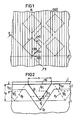
- FIG. 1 shows a top view of part of the surface of a semiconductor component with a defined overhead ignition voltage, into which depressions are etched using an etching mask.
- Anisotropic etching follows after the application of a mask with the shape and orientation of the mask opening according to the invention.
- the etching must be anisotropic so that the regularity of the crystal lattice structure is transferred to the recess geometry.
- Most such anisotropic etching solutions act quickly in the crystal direction perpendicular to the (110) plane and more slowly in the crystal direction perpendicular to the (100) plane. In the direction perpendicular to the (111) plane, the crystal is not (or only very slowly) degraded by anisotropic etchants.
- the etching process itself is known from the article by Angell, Terry and Barth "Micromechanics from Silicon", in the journal Spektrum dermaschine, June 1983, in particular page 41.
- FIG. 2 shows a section along the I-II line shown in FIG. 1, the truncated pyramid or pyramid-shaped depression V PS or V p now arises when using an etching mask 3 with a square opening M ⁇ of edge length a and one ⁇ 110 ⁇ opening orientation with respect to the ⁇ 100 ⁇ material 1 and 2.
- the doping interfaces D PS and D P which follow the shape of the depressions, separate the region 2, which is doped on the recess side and is x pn thick, from the base material 1, which is doped differently thereto.
- the angle ⁇ occurs only in the case of a truncated pyramidal depression V PS and is enclosed by one of each of the four ⁇ 111 ⁇ crystal planes and the bottom surface of the truncated pyramidal depression, the angle ⁇ represents the apex angle of the pyramid and is in each case by two of the four ⁇ 111 ⁇ -Crystal planes included.
- a plurality of mask openings can be provided, for example to enable higher current values, this then also corresponds to that in FIG. 2 depressions indicated by dashed lines V P , or V PS,.
- a truncated pyramid-shaped depression is sought instead of a pyramid-shaped depression, this can be achieved by simply increasing the edge length a of the mask opening M ⁇ .
- the etchant and mask are removed.
- doping is carried out only at this point on the recess side, so that a doping interface follows the surface contour and is shifted into the base material depending on the doping depth.
- a doping interface D P or D PS is formed.
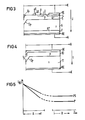
- FIG. 3 represents an overhead ignition-resistant thyristor with a fixed overhead ignition voltage, which consists of doped semiconductor material. It has four layers of alternating doping.
- the first layer which forms the emitter 4 and the auxiliary emitter 8, consists of n+-doped material and is electrically conductively connected to the cathode electrode KE.
- a p-base layer 5 adjoins the emitter and an n-base layer 6 adjoins this.
- the gate electrode GE is electrically conductively connected to the p-base layer 5 and the electrically conductive connection 9, which connects the auxiliary emitter 8 to the p-base layer 5.
- the gate electrode GE is connected to the gate terminal G
- the cathode electrode KE is electrical to the cathode terminal K connected conductively and the same applies to the anode electrode AE, which is connected to the anode terminal A.
- a voltage U is present between terminals K and A.
- the thyristor has a pyramid-shaped depression V P in a central region of the surface and can be produced particularly advantageously using the method according to the invention.
- the doping interface D P which separates the p-base layer 5 from the n-base layer 6, is therefore no longer flat, but follows the doping profile V P at a distance from the doping depth.
- the doping concentration gradient between p-base layer 5 and n-base layer 6 creates a space charge zone in this area, which in turn causes an electric field strength.
- the electrical field strength and thus also the overhead ignition voltage depend on the recess geometry and the doping profile. Due to the applied voltage U, a field strength arises in the region of the depression, which leads to a local avalanche breakdown and thus to a base current in the direction of the gate and ignition structures 8, 9. If there is no ignition structure 8, 9, the base current flows in the direction of the gate and emitter 4. In order for the thyristor to ignite quickly as a result of the avalanche breakdown current, several depressions can be provided, as already indicated in FIGS. 1 and 2.
- FIG. 1 A power diode with a fixed overhead ignition voltage is shown in FIG.
- the power diode consists of a p-doped layer 10 and an adjacent n-doped layer 11, the p-doped layer 10 being electrically conductively connected to the anode electrode AE and the anode terminal A and the n-doped layer 11 being electrically conductively connected to the Cathode electrode KE and the cathode terminal K is connected.
- the depression V P can be covered by a metallization layer both in the thyristor and in the power diode; As can be seen from FIG. 4, the metallization for producing the anode electrode has no cutouts in the region of the depression. As already explained in FIG.
- FIG. 5 shows the defined setting of an overhead ignition voltage U BO (break over voltage) for the two cases of the truncated pyramid and the pyramid, the doping depth x pn being regarded as fixed.
- U BO break over voltage
- the overhead ignition voltage is largely independent of the trough depth h and depends only on whether it is a truncated pyramid or truncated pyramid.
- the overhead ignition voltage of a semiconductor component can be set reproducibly in a defined manner. In the latter case, that is for h much larger x pn , the overhead ignition voltage is even independent on the depth of the trough and only depends on the type of deepening.
Landscapes
- Thyristors (AREA)
Abstract
Die Erfindung betrifft ein Verfahren zur definierten Spannungseinstellung bei überkopfzündfesten Halbleiterbauelementen, mit definierter Überkopfzündspannung, wobei an einer dafür vorgesehenen Stelle, mit Hilfe einer Vertiefung VP bzw. VPS in der Oberfläche, ein darunterliegendes Dotierungsgebiet 2 so gestaltet wird, daß es der Vertiefungskontur im Bereich unterhalb der Vertiefung folgt und sich die Dotierungsgrenzfläche DP bzw. DPS ausbilden. Ist die Vertiefungsform fest vorgegeben, so hängt damit die Überkopfzündspannung nur noch vom gut zu beherrschenden Dotierungsprofil ab und kann dadurch definiert und reproduzierbar eingestellt werden. Erfindungsgemäß kann eine fest vorgegebene, zum Beispiel pyramiden- bzw. pyramidenstumpfförmige Vertiefung, durch die Wahl des Wafermaterials, durch die Form und Orientierung der Maskenöffnung und bei anisotroper Ätzung, auf einfache Weise erzeugt werden. Wird anschließend von der Seite der Vertiefung aus dotiert, so entsteht ein entsprechend der Vertiefung definiert geformtes Dotierungsgebiet.The invention relates to a method for a defined voltage setting in semiconductor components which are resistant to overhead ignition, with a defined overhead ignition voltage, a doping region 2 underneath being designed at a location provided for this purpose with the aid of a depression V P or V PS in the surface so that it corresponds to the depression contour in the The area below the depression follows and the doping interface D P or D PS form. If the shape of the recess is fixed, the overhead ignition voltage only depends on the doping profile that is easy to control and can thus be defined and reproducibly set. According to the invention, a predetermined, for example pyramid or truncated pyramid-shaped depression can be produced in a simple manner by the choice of the wafer material, by the shape and orientation of the mask opening and in the case of anisotropic etching. If doping is then carried out from the side of the depression, a doping region is formed which is defined in accordance with the depression.
Description
Verfahren zur definierten Spannungseinstellung bei überkopfzündfesten Halbleiterbauelementen und Halbleiterbauelemente mit definierter Überkopfzündspannung.Process for the defined voltage setting in the case of semiconductor components which are resistant to overhead ignition and semiconductor components having a defined overhead ignition voltage.
Die Erfindung bezieht sich auf ein Verfahren nach dem Oberbegriff des Patentanspruchs 1 und ein Halbleiterbauelement nach dem Oberbegriff des Patentanspruchs 6.The invention relates to a method according to the preamble of patent claim 1 and a semiconductor component according to the preamble of patent claim 6.
Aus den Konferenzunterlagen zur "IEEE International Conference Thyristors and Variable and Static Euqipment for AC and DC Transmission", 30.11.1981 bis 03.12.1981 in London, aus der darin enthaltenen Veröffentlichung von V. A. K. Temple (GE) zum Thema "Advanced Light Triggered Thyristors For Electric Power Systems", insbesondere Seite 88 und Seite 91, Figur 10 ist ein Verfahren und eine Thyristorstruktur dieser Art bekannt. Bei dem von V. A. K. Temple erwähnten Verfahren werden ohne spezielle Berücksichtigung der Vertiefungsgeometrie, mehrere Vertiefungen in das vollständig dotierte Halbleiterbauelement geätzt, dadurch ergeben sich aufgrund der dabei schlecht zu beherrschenden Verfahrensparameter nicht definiert reproduzierbare Überkopfspannungen.From the conference documents for the "IEEE International Conference Thyristors and Variable and Static Equipment for AC and DC Transmission", November 30, 1981 to December 3, 1981 in London, from the publication contained therein by VAK Temple (GE) on "Advanced Light Triggered Thyristors For Electric Power Systems ", in particular page 88 and page 91, FIG. 10, a method and a thyristor structure of this type are known. In the process mentioned by V. A. K. Temple, several recesses are etched into the fully doped semiconductor component without special consideration of the recess geometry, which results in undefined reproducible overhead voltages due to the process parameters that are difficult to control.
Der Erfindung liegt die Aufgabe zugrunde, eine feste Überkopfzündspannung des Halbleiterbauelements so einzustellen, daß eine mittlere Schwankungsbreite aufgrund nicht trivial zu beherrschender Parameter minimal ist. Dies wird erfindungsgemäß bei einem Verfahren der eingangs angedeuteten Art durch eine Ausbildung nach dem kennzeichnenden Teil von Anspruch 1 erreicht.The object of the invention is to set a fixed overhead ignition voltage of the semiconductor component in such a way that an average fluctuation range is minimal due to parameters which cannot be trivially controlled. This is achieved according to the invention in a method of the type indicated at the outset by training according to the characterizing part of claim 1.
Die Erfindung zeichnet sich insbesondere durch Einfachheit und durch gute Reproduzierbarkeit einer gewünschten Überkopfzündspannung aus.The invention is particularly characterized by simplicity and good reproducibility of a desired overhead ignition voltage.
Die Patentansprüche 2 bis 5 sind auf bevorzugte Weiterbildungen des erfindungsgemäßen Verfahrens gerichtet.
Die Patentansprüche 6 bis 8 betreffen ein Halbleiterbauelement mit definierter Überkopfzündspannung, das mit Vorteil nach einem der Ansprüche 1 bis 5 herstellbar ist.Claims 6 to 8 relate to a semiconductor component with a defined overhead ignition voltage, which can advantageously be produced according to one of Claims 1 to 5.
Die Erfindung wird nachfolgend anhand der Zeichnung näher erläutert. Dabei zeigt
- Figur 1
- eine Darstellung der beim Verfahren nach der Erfindung verwendeten Ätzmaskenorientierung relativ zur Orientierung der Kristallgitterebenen (Verwendung von Miller-Indizes),
Figur 2- Vertiefungen und Dotierungsverläufe bei Anwendung des erfindungsgemäßen Verfahrens,
- Figur 3
- einen Aufbau eines Thyristors mit Vertiefungen nach
Figur 2, - Figur 4
- einen Aufbau einer Leistungsdiode mit Vertiefungen nach
Figur 2 und - Figur 5
- die bei den Vertiefungen (Mulden) nach
Figur 2 erreichbare Überkopfzündspannung UBO (break over voltage), bei fester Dotierungstiefe xpn, in Abhängigkeit von der Muldentiefe h und der Muldenform P (Pyramide) bzw. PS (Pyramidenstumpf).
- Figure 1
- a representation of the etching mask orientation used in the method according to the invention relative to the orientation of the crystal lattice planes (use of Miller indices),
- Figure 2
- Wells and doping courses when using the method according to the invention,
- Figure 3
- a structure of a thyristor with depressions according to Figure 2,
- Figure 4
- a structure of a power diode with depressions according to Figure 2 and
- Figure 5
- the over head ignition voltage U BO (break over voltage) which can be achieved in the depressions (troughs) according to FIG. 2, with a fixed doping depth x pn , depending on the trough depth h and the trough shape P (pyramid) or PS (truncated pyramid).
Figur 1 zeigt in Draufsicht einen Teil der Oberfläche eines Halbleiter Bauelements mit definierter Überkopfzündspannung, in die mit Hilfe einer Ätzmaske Vertiefungen eingeätzt werden. Dabei wird zuerst, in einer bevorzugten Weiterbildung des erfindungsgemäßen Verfahrens, eine Maske mit quadratischer Maskenöffnung MÖ, der Kantenlänge a, so auf ein {100} -Halbleitermaterial aufgebracht, daß eine Kante der Maskenöffnung parallel zur 〈110〉 -Richtung im Kristall ist. Gestrichelt angedeutet sind weitere Maskenöffnungen dieser Art.FIG. 1 shows a top view of part of the surface of a semiconductor component with a defined overhead ignition voltage, into which depressions are etched using an etching mask. First, in a preferred development of the method according to the invention, a mask with a square mask opening MÖ, the edge length a, is applied to a {100} semiconductor material such that one edge of the mask opening is parallel to the 〈110〉 direction in the crystal. Further mask openings of this type are indicated by dashed lines.
Nach dem Aufbringen einer Maske mit erfindungsgemäßer Form und Orientierung der Maskenöffnung folgt eine anisotrope Ätzung. Die Ätzung muß anisotrop erfolgen, damit sich die Regularität der Kristallgitterstruktur auf die Vertiefungsgeometrie überträgt. Die meisten solcher anisotroper Ätzlösungen, wirken schnell in Kristallrichtung senkrecht zur (110)-Ebene und langsamer in die Kristallrichtung senkrecht zur (100)-Ebene. In Richtung senkrecht zur (111)-Ebene wird der Kristall von anisotropen Ätzmitteln nicht (oder nur sehr langsam) abgebaut. Das Ätzverfahren selbst ist aus dem Artikel von Angell, Terry und Barth "Mikromechanik aus Silicium", in der Zeitschrift Spektrum der Wissenschaft, Juni 1983, insbesondere Seite 41 bekannt.Anisotropic etching follows after the application of a mask with the shape and orientation of the mask opening according to the invention. The etching must be anisotropic so that the regularity of the crystal lattice structure is transferred to the recess geometry. Most such anisotropic etching solutions act quickly in the crystal direction perpendicular to the (110) plane and more slowly in the crystal direction perpendicular to the (100) plane. In the direction perpendicular to the (111) plane, the crystal is not (or only very slowly) degraded by anisotropic etchants. The etching process itself is known from the article by Angell, Terry and Barth "Micromechanics from Silicon", in the journal Spektrum der Wissenschaft, June 1983, in particular page 41.
Die Figur 2 stellt einen Schnitt entlang der in Figur 1 gezeigten I-II-Linie dar, die gezeigte pyramidenstumpf- bzw. pyramidenförmige Vertiefung VPS bzw. Vp, entsteht nun bei Verwendung einer Ätzmaske 3 mit quadratischer Öffnung MÖ der Kantenlänge a und einer 〈110〉 -Öffnungsorientierung bezüglich des {100} -Materials 1 und 2. Die der Form der Vertiefungen folgenden Dotierungsgrenzflächen DPS bzw. DP trennen das vertiefungsseitig dotierte und xpn dicke Gebiet 2 von dem dazu unterschiedlich dotierten Grundmaterial 1. Der Winkel α tritt nur im Fall einer pyramidenstumpfförmigen Vertiefung VPS in Erscheinung und wird von jeweils einer der vier {111} -Kristallebenen und der Bodenfläche der pyramidenstumpfförmigen Vertiefung eingeschlossen, der Winkel β stellt den Spitzenwinkel der Pyramide dar und wird durch jeweils zwei der vier {111} -Kristallebenen eingeschlossen.FIG. 2 shows a section along the I-II line shown in FIG. 1, the truncated pyramid or pyramid-shaped depression V PS or V p now arises when using an etching mask 3 with a square opening MÖ of edge length a and one 〈110〉 opening orientation with respect to the {100}
Die Winkel betragen ungefähr:
![]()
![]()
The angles are approximately:
![]()
![]()
Wie in Figur 1 gestrichelt angedeutet, können mehrere Maskenöffnungen vorgesehen werden, um zum Beispiel höhere Stromwerte zu ermöglichen, dies entspricht dann den in Figur 2 ebenfalls gestrichelt angedeuteten Vertiefungen VP, bzw. VPS,.As indicated by dashed lines in FIG. 1, a plurality of mask openings can be provided, for example to enable higher current values, this then also corresponds to that in FIG. 2 depressions indicated by dashed lines V P , or V PS,.
Wird bei vorgegebener, durch die Ätzdauer bestimmten Ätztiefe hPS bzw. hP, statt einer pyramidenförmigen Vertiefung eine pyramidenstumpfförmige angestrebt, so kann dies durch einfaches Vergrößern der Kantenlänge a der Maskenöffnung MÖ erreicht werden. Nach Ablauf der Ätzdauer wird das Ätzmittel und die Maske entfernt. Erfindungsgemäß wird erst zu diesem Zeitpunkt vertiefungsseitig eine Dotierung vorgenommen, so daß sich eine, je nach Dotierungstiefe ins Grundmaterial verschobene, der Oberflächenkontur folgende Dotierungsgrenzfläche ergibt. Im Fall der in Figur 2 gezeigten Vertiefung VP bzw. VPS wird eine Dotierungsgrenzfläche DP bzw. DPS gebildet.If, for a given etching depth h PS or h P determined by the etching duration, a truncated pyramid-shaped depression is sought instead of a pyramid-shaped depression, this can be achieved by simply increasing the edge length a of the mask opening MÖ. After the etching period, the etchant and mask are removed. According to the invention, doping is carried out only at this point on the recess side, so that a doping interface follows the surface contour and is shifted into the base material depending on the doping depth. In the case of the depression V P or V PS shown in FIG. 2, a doping interface D P or D PS is formed.
Zur Fertigstellung des Halbleiterbauelements mit fester Überkopfzündspannung folgen weitere Schritte, die aber nicht mehr Gegenstand der Erfindung sind.Further steps follow to complete the semiconductor component with a fixed overhead ignition voltage, but these are no longer the subject of the invention.
Es ist von Vorteil überkopfzündfeste Halbleiterbauelemente mit definierter Überkopfzündspannung, wie zum Beispiel Leistungsdioden und Thyristoren, nach dem erfindungsgemäßen Verfahren herzustellen.It is advantageous to manufacture semiconductor components which are resistant to overhead ignition and have a defined overhead ignition voltage, such as, for example, power diodes and thyristors, using the method according to the invention.
Figur 3 stellt dabei einen überkopfzündfesten Thyristor mit fester Überkopfzündspannung dar, der aus dotiertem Halbleitermaterial besteht. Er weist vier Schichten abwechselnder Dotierung auf. Die erste Schicht, die den Emitter 4 und dem Hilfsemitter 8 bildet, besteht aus n⁺ -dotiertem Material und ist elektrisch leitend mit der Kathodenelektrode KE verbunden. An die Emitter schließt sich eine p-Basisschicht 5 an und an diese wiederum eine n-Basisschicht 6. An die n-Basisschicht 6 grenzt die p⁺-Emitterschicht 7, die elektrisch leitend mit der Anodenelektrode AE verbunden ist. Weitere metallische Bereiche an der kathodenseitigen Oberfläche des Thyristors sind die Gateelektrode GE, die elektrisch leitend mit der p-Basisschicht 5 verbunden ist und die elektrisch leitende Verbindung 9, die den Hilfsemitters 8 mit der p-Basisschicht 5 verbindet. Die Gateelektrode GE ist mit dem Gateanschluß G verbunden, die Kathodenelektrode KE ist mit der Kathodenanschlußklemme K elektrisch leitend verbunden und gleiches gilt für die Anodenelektrode AE, die mit der Anodenanschlußklemme A verbunden ist. Zwischen den Klemmen K und A liegt eine Spannung U an. Der Thyristor weist in einem zentralen Bereich der Oberfläche eine pyramidenförmige Vertiefung VP auf und kann mit Hilfe des erfindungsgemäßen Verfahrens besonders vorteilhaft hergestellt werden. Die Dotierungsgrenzfläche DP, welche die p-Basisschicht 5 von der n-Basisschicht 6 trennt, ist somit nicht mehr eben, sondern folgt im Abstand der Dotierungstiefe dem Dotierungsprofil VP. Das Dotierungskonzentrationsgefälle zwischen p-Basisschicht 5 und n-Basisschicht 6 läßt eine Raumladungszone in diesem Bereich entstehen, diese wiederum bewirkt eine elektrische Feldstärke. Die elektrische Feldstärke und damit auch die Überkopfzündspannung sind von der Vertiefungsgeometrie und vom Dotierungsprofil abhängig. Aufgrund der angelegten Spannung U entsteht eine Feldstärke im Bereich der Vertiefung, die zu einem lokalen Lawinendurchbruch und damit zu einem Basisstrom in Richtung Gate und Zündstrukturen 8, 9 führt. Ist keine Zündstruktur 8, 9 vorhanden, so fließt der Basisstrom in Richtung Gate und Emitter 4. Damit ein Zünden des Thyristors infolge des Lawinendurchbruchstromes schnell erfolgt, können mehrere Vertiefungen, wie bereits in Figur 1 und 2 angedeutet, vorgesehen werden.FIG. 3 represents an overhead ignition-resistant thyristor with a fixed overhead ignition voltage, which consists of doped semiconductor material. It has four layers of alternating doping. The first layer, which forms the emitter 4 and the
In Figur 4 wird eine Leistungsdiode mit fester Überkopfzündspannung dargestellt. Die Leistungsdiode besteht aus einer p-dotierten Schicht 10 und einer daran angrenzenden n-dotierten Schicht 11, wobei die p-dotierte Schicht 10 elektrisch leitend mit der Anodenelektrode AE und der Anodenklemme A verbunden ist und die n-dotierte Schicht 11 elektrisch leitend mit der Kathodenelektrode KE und der Kathodenklemme K verbunden ist. Die Vertiefung VP kann sowohl beim Thyristor als auch bei der Leistungsdiode durch eine Metallisierungsschicht abgedeckt werden; wie aus Figur 4 ersichtlich, besitzt die Metallisierung zur Herstellung der Anodenelektrode keinerlei Aussparungen im Bereich der Vertiefung. Unterhalb der Vertiefung VP befindet sich, wie in Figur 3 bereits erläutert, eine der Oberflächenkontur folgende Dotierungsgrenzfläche DP. Wird eine genügend hohe Spannung U zwischen den Klemmen A und K angelegt, so kann ein Lawinendurchbruch örtlich, im Bereich der Vertiefung, festgelegt werden. Ist der Ort des Lawinendurchbruchs bekannt, können entsprechende Schutzmaßnahmen gegen thermische Überlastung getroffen werden.A power diode with a fixed overhead ignition voltage is shown in FIG. The power diode consists of a p-doped
Figur 5 stellt die definierte Einstellung einer Überkopfzündspannung UBO (break over voltage) für die beiden Fälle des Pyramidenstumpfes und der Pyramide dar, wobei die Dotierungstiefe xpn als fest anzusehen ist. Figur 5 zeigt, daß die Überkopfzündspannung bei pyramidenförmiger Vertiefung stets niedriger ist als bei pyramidenstumpfförmiger Vertiefung. Für den Bereich A, also für sehr kleine Werte von h, fällt UBO von einem Maximalwert bei h = 0 in Richtung zu größeren h-Werten ab.FIG. 5 shows the defined setting of an overhead ignition voltage U BO (break over voltage) for the two cases of the truncated pyramid and the pyramid, the doping depth x pn being regarded as fixed. FIG. 5 shows that the overhead ignition voltage is always lower in the case of a pyramid-shaped depression than in the case of a truncated pyramid-shaped depression. For area A, that is, for very small values of h, U BO drops from a maximum value at h = 0 towards larger h values.
Für den Bereich B, also h sehr viel größer als xpn, ist die Überkopfzündspannung weitgehend unabhängig von der Muldentiefe h und hängt nur noch davon ab, ob es sich um eine pyramiden- oder pyramidenstumpfförmige Mulde handelt.For area B, i.e. h is much larger than x pn , the overhead ignition voltage is largely independent of the trough depth h and depends only on whether it is a truncated pyramid or truncated pyramid.
Es gelten folgende Zusammenhänge:
Für den Bereich h kleiner, gleich xpn (Bereich A) wird
![]()
![]()
Für den Bereich h sehr viel größer xpn (Bereich B) wird
![]()
![]()
The following relationships apply:
For the area h less than or equal to x pn (area A)
![]()
![]()
For area h, x pn (area B) becomes much larger
![]()
![]()
Dies zeigt, daß bei fester Vorgabe des gut kontrollierbaren Dotierungsprofils mit der Dotierungstiefe xpn, die Überkopfzündspannung eines Halbleiterbauelementes definiert reproduzierbar eingestellt werden kann. Im letzteren Fall, also für h sehr viel größer xpn, ist die Überkopfzündspannung sogar unabhängig von der Muldentiefe und hängt nur noch von der Art der Vertiefungsform ab.This shows that with a fixed specification of the easily controllable doping profile with the doping depth x pn , the overhead ignition voltage of a semiconductor component can be set reproducibly in a defined manner. In the latter case, that is for h much larger x pn , the overhead ignition voltage is even independent on the depth of the trough and only depends on the type of deepening.
Claims (9)
Applications Claiming Priority (2)
| Application Number | Priority Date | Filing Date | Title |
|---|---|---|---|
| DE4007816 | 1990-03-12 | ||
| DE4007816 | 1990-03-12 |
Publications (3)
| Publication Number | Publication Date |
|---|---|
| EP0446438A2 true EP0446438A2 (en) | 1991-09-18 |
| EP0446438A3 EP0446438A3 (en) | 1992-04-22 |
| EP0446438B1 EP0446438B1 (en) | 1996-05-01 |
Family
ID=6402008
Family Applications (1)
| Application Number | Title | Priority Date | Filing Date |
|---|---|---|---|
| EP90123238A Expired - Lifetime EP0446438B1 (en) | 1990-03-12 | 1990-12-04 | Method of setting the voltage in a well-defined manner in semiconductor devices which withstand voltage-breakover firing and semiconductor devices having a well-defined breakover voltage |
Country Status (3)
| Country | Link |
|---|---|
| EP (1) | EP0446438B1 (en) |
| JP (1) | JP3165459B2 (en) |
| DE (1) | DE59010309D1 (en) |
Families Citing this family (1)
| Publication number | Priority date | Publication date | Assignee | Title |
|---|---|---|---|---|
| JP2007134384A (en) * | 2005-11-08 | 2007-05-31 | Renesas Technology Corp | Constant voltage diode |
Family Cites Families (2)
| Publication number | Priority date | Publication date | Assignee | Title |
|---|---|---|---|---|
| JPH01136369A (en) * | 1987-11-21 | 1989-05-29 | Toshiba Corp | Manufacture of semiconductor device having overvoltage protective function |
| EP0446439B1 (en) * | 1990-03-12 | 1996-07-24 | Siemens Aktiengesellschaft | Thyristor having a light ignition structure with low reflection |
-
1990
- 1990-12-04 EP EP90123238A patent/EP0446438B1/en not_active Expired - Lifetime
- 1990-12-04 DE DE59010309T patent/DE59010309D1/en not_active Expired - Lifetime
-
1991
- 1991-03-11 JP JP07239691A patent/JP3165459B2/en not_active Expired - Fee Related
Also Published As
| Publication number | Publication date |
|---|---|
| DE59010309D1 (en) | 1996-06-05 |
| JPH04219979A (en) | 1992-08-11 |
| EP0446438B1 (en) | 1996-05-01 |
| EP0446438A3 (en) | 1992-04-22 |
| JP3165459B2 (en) | 2001-05-14 |
Similar Documents
| Publication | Publication Date | Title |
|---|---|---|
| DE19605633B4 (en) | Method for producing diodes with improved breakdown voltage characteristics | |
| DE69625815T2 (en) | BREAKTHROUGH LOW-VOLTAGE SUPPRESSOR WITH DOUBLE-LAYER BASE | |
| DE60028134T2 (en) | Edge termination for silicon power arrangements | |
| DE69005805T2 (en) | Planar edge termination for high stresses using a penetration-inhibiting implant. | |
| WO1997001189A1 (en) | Solar cell with an emitter having a surface texture and process for manufacturing the same | |
| DE2241600A1 (en) | HIGH VOLTAGE P-N TRANSITION AND ITS APPLICATION IN SEMICONDUCTOR SWITCHING ELEMENTS, AND THE PROCESS FOR ITS MANUFACTURING | |
| DE4320780B4 (en) | Semiconductor device and method of manufacture | |
| DE10235198B4 (en) | Power semiconductor rectifier with annular trenches | |
| DE2712114C2 (en) | Switchable semiconductor device and method for making the same | |
| DE1208411B (en) | Breakdown-insensitive semiconductor rectifier with a zone of higher specific resistance | |
| DE7016282U (en) | SEMI-CONDUCTOR SWITCHING DEVICE. | |
| DE10203820B4 (en) | Semiconductor component and method for its production | |
| DE19930781B4 (en) | Metal-semiconductor contact diode and method of making the same | |
| EP0332955A2 (en) | Thyristor having a large forward and reverse blocking capability, and method of making the same | |
| EP0095658A2 (en) | Planar semiconductor device and method of making the same | |
| EP1139432A2 (en) | Schottky diode | |
| DE2205991A1 (en) | Method for manufacturing a semiconductor component | |
| EP0446438B1 (en) | Method of setting the voltage in a well-defined manner in semiconductor devices which withstand voltage-breakover firing and semiconductor devices having a well-defined breakover voltage | |
| DE2238564B2 (en) | Thyristor | |
| EP0164645A2 (en) | Silicon semiconductor device having a contour of the border formed by chemical attack, and process for manufacturing this device | |
| DE2625856B2 (en) | ||
| DE2356674C2 (en) | Semiconductor component with a disk-shaped semiconductor body | |
| DE112016001599T5 (en) | Semiconductor device and method of manufacturing a semiconductor device | |
| WO1999009597A1 (en) | High voltage component and method for making same | |
| DE112017008002T5 (en) | Semiconductor device |
Legal Events
| Date | Code | Title | Description |
|---|---|---|---|
| PUAI | Public reference made under article 153(3) epc to a published international application that has entered the european phase |
Free format text: ORIGINAL CODE: 0009012 |
|
| 17P | Request for examination filed |
Effective date: 19901220 |
|
| AK | Designated contracting states |
Kind code of ref document: A2 Designated state(s): CH DE GB LI SE |
|
| PUAL | Search report despatched |
Free format text: ORIGINAL CODE: 0009013 |
|
| AK | Designated contracting states |
Kind code of ref document: A3 Designated state(s): CH DE GB LI SE |
|
| 17Q | First examination report despatched |
Effective date: 19941205 |
|
| GRAH | Despatch of communication of intention to grant a patent |
Free format text: ORIGINAL CODE: EPIDOS IGRA |
|
| GRAA | (expected) grant |
Free format text: ORIGINAL CODE: 0009210 |
|
| AK | Designated contracting states |
Kind code of ref document: B1 Designated state(s): CH DE GB LI SE |
|
| REG | Reference to a national code |
Ref country code: CH Ref legal event code: NV Representative=s name: SIEMENS SCHWEIZ AG |
|
| REF | Corresponds to: |
Ref document number: 59010309 Country of ref document: DE Date of ref document: 19960605 |
|
| GBT | Gb: translation of ep patent filed (gb section 77(6)(a)/1977) |
Effective date: 19960705 |
|
| PLBE | No opposition filed within time limit |
Free format text: ORIGINAL CODE: 0009261 |
|
| STAA | Information on the status of an ep patent application or granted ep patent |
Free format text: STATUS: NO OPPOSITION FILED WITHIN TIME LIMIT |
|
| 26N | No opposition filed | ||
| REG | Reference to a national code |
Ref country code: GB Ref legal event code: IF02 |
|
| PGFP | Annual fee paid to national office [announced via postgrant information from national office to epo] |
Ref country code: CH Payment date: 20081215 Year of fee payment: 19 |
|
| REG | Reference to a national code |
Ref country code: CH Ref legal event code: PCAR Free format text: SIEMENS SCHWEIZ AG;INTELLECTUAL PROPERTY FREILAGERSTRASSE 40;8047 ZUERICH (CH) |
|
| PGFP | Annual fee paid to national office [announced via postgrant information from national office to epo] |
Ref country code: SE Payment date: 20081212 Year of fee payment: 19 |
|
| PGFP | Annual fee paid to national office [announced via postgrant information from national office to epo] |
Ref country code: GB Payment date: 20081216 Year of fee payment: 19 |
|
| PGFP | Annual fee paid to national office [announced via postgrant information from national office to epo] |
Ref country code: DE Payment date: 20100222 Year of fee payment: 20 |
|
| EUG | Se: european patent has lapsed | ||
| REG | Reference to a national code |
Ref country code: CH Ref legal event code: PL |
|
| GBPC | Gb: european patent ceased through non-payment of renewal fee |
Effective date: 20091204 |
|
| PG25 | Lapsed in a contracting state [announced via postgrant information from national office to epo] |
Ref country code: LI Free format text: LAPSE BECAUSE OF NON-PAYMENT OF DUE FEES Effective date: 20091231 Ref country code: CH Free format text: LAPSE BECAUSE OF NON-PAYMENT OF DUE FEES Effective date: 20091231 |
|
| PG25 | Lapsed in a contracting state [announced via postgrant information from national office to epo] |
Ref country code: GB Free format text: LAPSE BECAUSE OF NON-PAYMENT OF DUE FEES Effective date: 20091204 |
|
| PG25 | Lapsed in a contracting state [announced via postgrant information from national office to epo] |
Ref country code: SE Free format text: LAPSE BECAUSE OF NON-PAYMENT OF DUE FEES Effective date: 20091205 |
|
| PG25 | Lapsed in a contracting state [announced via postgrant information from national office to epo] |
Ref country code: DE Free format text: LAPSE BECAUSE OF EXPIRATION OF PROTECTION Effective date: 20101204 |