EP0446438A2 - Méthode pour régler la tension d'une manière bien définie dans des dispositifs semi-conducteurs supportant les amorçages par retournement et dispositifs semi-conducteurs à tension de retournement bien définie - Google Patents
Méthode pour régler la tension d'une manière bien définie dans des dispositifs semi-conducteurs supportant les amorçages par retournement et dispositifs semi-conducteurs à tension de retournement bien définie Download PDFInfo
- Publication number
- EP0446438A2 EP0446438A2 EP90123238A EP90123238A EP0446438A2 EP 0446438 A2 EP0446438 A2 EP 0446438A2 EP 90123238 A EP90123238 A EP 90123238A EP 90123238 A EP90123238 A EP 90123238A EP 0446438 A2 EP0446438 A2 EP 0446438A2
- Authority
- EP
- European Patent Office
- Prior art keywords
- depression
- voltage
- semiconductor component
- etching
- doping
- Prior art date
- Legal status (The legal status is an assumption and is not a legal conclusion. Google has not performed a legal analysis and makes no representation as to the accuracy of the status listed.)
- Granted
Links
Images
Classifications
-
- H—ELECTRICITY
- H10—SEMICONDUCTOR DEVICES; ELECTRIC SOLID-STATE DEVICES NOT OTHERWISE PROVIDED FOR
- H10P—GENERIC PROCESSES OR APPARATUS FOR THE MANUFACTURE OR TREATMENT OF DEVICES COVERED BY CLASS H10
- H10P50/00—Etching of wafers, substrates or parts of devices
- H10P50/60—Wet etching
- H10P50/64—Wet etching of semiconductor materials
- H10P50/642—Chemical etching
- H10P50/644—Anisotropic liquid etching
-
- H—ELECTRICITY
- H10—SEMICONDUCTOR DEVICES; ELECTRIC SOLID-STATE DEVICES NOT OTHERWISE PROVIDED FOR
- H10D—INORGANIC ELECTRIC SEMICONDUCTOR DEVICES
- H10D18/00—Thyristors
- H10D18/211—Thyristors having built-in localised breakdown or breakover regions, e.g. self-protected against destructive spontaneous firing
-
- H—ELECTRICITY
- H10—SEMICONDUCTOR DEVICES; ELECTRIC SOLID-STATE DEVICES NOT OTHERWISE PROVIDED FOR
- H10D—INORGANIC ELECTRIC SEMICONDUCTOR DEVICES
- H10D8/00—Diodes
- H10D8/20—Breakdown diodes, e.g. avalanche diodes
-
- H—ELECTRICITY
- H10—SEMICONDUCTOR DEVICES; ELECTRIC SOLID-STATE DEVICES NOT OTHERWISE PROVIDED FOR
- H10P—GENERIC PROCESSES OR APPARATUS FOR THE MANUFACTURE OR TREATMENT OF DEVICES COVERED BY CLASS H10
- H10P50/00—Etching of wafers, substrates or parts of devices
- H10P50/69—Etching of wafers, substrates or parts of devices using masks for semiconductor materials
- H10P50/691—Etching of wafers, substrates or parts of devices using masks for semiconductor materials for Group V materials or Group III-V materials
- H10P50/693—Etching of wafers, substrates or parts of devices using masks for semiconductor materials for Group V materials or Group III-V materials characterised by their size, orientation, disposition, behaviour or shape, in horizontal or vertical plane
Definitions
- the invention relates to a method according to the preamble of patent claim 1 and a semiconductor component according to the preamble of patent claim 6.
- the object of the invention is to set a fixed overhead ignition voltage of the semiconductor component in such a way that an average fluctuation range is minimal due to parameters which cannot be trivially controlled. This is achieved according to the invention in a method of the type indicated at the outset by training according to the characterizing part of claim 1.
- the invention is particularly characterized by simplicity and good reproducibility of a desired overhead ignition voltage.
- Claims 2 to 5 are directed to preferred developments of the method according to the invention.
- Claims 6 to 8 relate to a semiconductor component with a defined overhead ignition voltage, which can advantageously be produced according to one of Claims 1 to 5.
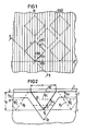
- FIG. 1 shows a top view of part of the surface of a semiconductor component with a defined overhead ignition voltage, into which depressions are etched using an etching mask.
- Anisotropic etching follows after the application of a mask with the shape and orientation of the mask opening according to the invention.
- the etching must be anisotropic so that the regularity of the crystal lattice structure is transferred to the recess geometry.
- Most such anisotropic etching solutions act quickly in the crystal direction perpendicular to the (110) plane and more slowly in the crystal direction perpendicular to the (100) plane. In the direction perpendicular to the (111) plane, the crystal is not (or only very slowly) degraded by anisotropic etchants.
- the etching process itself is known from the article by Angell, Terry and Barth "Micromechanics from Silicon", in the journal Spektrum dermaschine, June 1983, in particular page 41.
- FIG. 2 shows a section along the I-II line shown in FIG. 1, the truncated pyramid or pyramid-shaped depression V PS or V p now arises when using an etching mask 3 with a square opening M ⁇ of edge length a and one ⁇ 110 ⁇ opening orientation with respect to the ⁇ 100 ⁇ material 1 and 2.
- the doping interfaces D PS and D P which follow the shape of the depressions, separate the region 2, which is doped on the recess side and is x pn thick, from the base material 1, which is doped differently thereto.
- the angle ⁇ occurs only in the case of a truncated pyramidal depression V PS and is enclosed by one of each of the four ⁇ 111 ⁇ crystal planes and the bottom surface of the truncated pyramidal depression, the angle ⁇ represents the apex angle of the pyramid and is in each case by two of the four ⁇ 111 ⁇ -Crystal planes included.
- a plurality of mask openings can be provided, for example to enable higher current values, this then also corresponds to that in FIG. 2 depressions indicated by dashed lines V P , or V PS,.
- a truncated pyramid-shaped depression is sought instead of a pyramid-shaped depression, this can be achieved by simply increasing the edge length a of the mask opening M ⁇ .
- the etchant and mask are removed.
- doping is carried out only at this point on the recess side, so that a doping interface follows the surface contour and is shifted into the base material depending on the doping depth.
- a doping interface D P or D PS is formed.
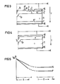
- FIG. 3 represents an overhead ignition-resistant thyristor with a fixed overhead ignition voltage, which consists of doped semiconductor material. It has four layers of alternating doping.
- the first layer which forms the emitter 4 and the auxiliary emitter 8, consists of n+-doped material and is electrically conductively connected to the cathode electrode KE.
- a p-base layer 5 adjoins the emitter and an n-base layer 6 adjoins this.
- the gate electrode GE is electrically conductively connected to the p-base layer 5 and the electrically conductive connection 9, which connects the auxiliary emitter 8 to the p-base layer 5.
- the gate electrode GE is connected to the gate terminal G
- the cathode electrode KE is electrical to the cathode terminal K connected conductively and the same applies to the anode electrode AE, which is connected to the anode terminal A.
- a voltage U is present between terminals K and A.
- the thyristor has a pyramid-shaped depression V P in a central region of the surface and can be produced particularly advantageously using the method according to the invention.
- the doping interface D P which separates the p-base layer 5 from the n-base layer 6, is therefore no longer flat, but follows the doping profile V P at a distance from the doping depth.
- the doping concentration gradient between p-base layer 5 and n-base layer 6 creates a space charge zone in this area, which in turn causes an electric field strength.
- the electrical field strength and thus also the overhead ignition voltage depend on the recess geometry and the doping profile. Due to the applied voltage U, a field strength arises in the region of the depression, which leads to a local avalanche breakdown and thus to a base current in the direction of the gate and ignition structures 8, 9. If there is no ignition structure 8, 9, the base current flows in the direction of the gate and emitter 4. In order for the thyristor to ignite quickly as a result of the avalanche breakdown current, several depressions can be provided, as already indicated in FIGS. 1 and 2.
- FIG. 1 A power diode with a fixed overhead ignition voltage is shown in FIG.
- the power diode consists of a p-doped layer 10 and an adjacent n-doped layer 11, the p-doped layer 10 being electrically conductively connected to the anode electrode AE and the anode terminal A and the n-doped layer 11 being electrically conductively connected to the Cathode electrode KE and the cathode terminal K is connected.
- the depression V P can be covered by a metallization layer both in the thyristor and in the power diode; As can be seen from FIG. 4, the metallization for producing the anode electrode has no cutouts in the region of the depression. As already explained in FIG.
- FIG. 5 shows the defined setting of an overhead ignition voltage U BO (break over voltage) for the two cases of the truncated pyramid and the pyramid, the doping depth x pn being regarded as fixed.
- U BO break over voltage
- the overhead ignition voltage is largely independent of the trough depth h and depends only on whether it is a truncated pyramid or truncated pyramid.
- the overhead ignition voltage of a semiconductor component can be set reproducibly in a defined manner. In the latter case, that is for h much larger x pn , the overhead ignition voltage is even independent on the depth of the trough and only depends on the type of deepening.
Landscapes
- Thyristors (AREA)
Applications Claiming Priority (2)
| Application Number | Priority Date | Filing Date | Title |
|---|---|---|---|
| DE4007816 | 1990-03-12 | ||
| DE4007816 | 1990-03-12 |
Publications (3)
| Publication Number | Publication Date |
|---|---|
| EP0446438A2 true EP0446438A2 (fr) | 1991-09-18 |
| EP0446438A3 EP0446438A3 (en) | 1992-04-22 |
| EP0446438B1 EP0446438B1 (fr) | 1996-05-01 |
Family
ID=6402008
Family Applications (1)
| Application Number | Title | Priority Date | Filing Date |
|---|---|---|---|
| EP90123238A Expired - Lifetime EP0446438B1 (fr) | 1990-03-12 | 1990-12-04 | Méthode pour régler la tension d'une manière bien définie dans des dispositifs semi-conducteurs supportant les amorçages par retournement et dispositifs semi-conducteurs à tension de retournement bien définie |
Country Status (3)
| Country | Link |
|---|---|
| EP (1) | EP0446438B1 (fr) |
| JP (1) | JP3165459B2 (fr) |
| DE (1) | DE59010309D1 (fr) |
Families Citing this family (1)
| Publication number | Priority date | Publication date | Assignee | Title |
|---|---|---|---|---|
| JP2007134384A (ja) * | 2005-11-08 | 2007-05-31 | Renesas Technology Corp | 定電圧ダイオード |
Family Cites Families (2)
| Publication number | Priority date | Publication date | Assignee | Title |
|---|---|---|---|---|
| JPH01136369A (ja) * | 1987-11-21 | 1989-05-29 | Toshiba Corp | 過電圧保護機能付半導体装置の製造方法 |
| EP0446439B1 (fr) * | 1990-03-12 | 1996-07-24 | Siemens Aktiengesellschaft | Thyristor comprenant une structure d'allumage par la lumière avec faible réflexion |
-
1990
- 1990-12-04 EP EP90123238A patent/EP0446438B1/fr not_active Expired - Lifetime
- 1990-12-04 DE DE59010309T patent/DE59010309D1/de not_active Expired - Lifetime
-
1991
- 1991-03-11 JP JP07239691A patent/JP3165459B2/ja not_active Expired - Fee Related
Also Published As
| Publication number | Publication date |
|---|---|
| DE59010309D1 (de) | 1996-06-05 |
| JPH04219979A (ja) | 1992-08-11 |
| EP0446438B1 (fr) | 1996-05-01 |
| EP0446438A3 (en) | 1992-04-22 |
| JP3165459B2 (ja) | 2001-05-14 |
Similar Documents
| Publication | Publication Date | Title |
|---|---|---|
| DE19605633B4 (de) | Verfahren zur Herstellung von Dioden mit verbesserter Durchbruchspannungscharakteristik | |
| DE69625815T2 (de) | Durchbruchtransierter niederspannungs-unterdrücker mit zweischichtiger basis | |
| DE60028134T2 (de) | Randabschluss für Silizium-Leistungsanordnungen | |
| DE69005805T2 (de) | Planarer Randabschluss für hohe Spannungen unter Benutzung eines durchgriffshemmenden Implantates. | |
| WO1997001189A1 (fr) | Cellule solaire a emetteur pourvu d'une texture superficielle et son procede de fabrication | |
| DE2241600A1 (de) | Hochspannungs-p-n-uebergang und seine anwendung in halbleiterschaltelementen, sowie verfahren zu seiner herstellung | |
| DE4320780B4 (de) | Halbleiteranordnung und Verfahren zur Herstellung | |
| DE10235198B4 (de) | Leistungs-Halbleitergleichrichter mit ringförmigen Gräben | |
| DE2712114C2 (de) | Schaltbare Halbleitervorrichtung und Verfahren zu ihrer Herstellung | |
| DE1208411B (de) | Durchschlagsunempfindlicher Halbleitergleichrichter mit einer Zone hoeheren spezifischen Widerstands | |
| DE7016282U (de) | Halbleiterschaltvorrichtung. | |
| DE10203820B4 (de) | Halbleiterbauelement und Verfahren zu dessen Herstellung | |
| DE19930781B4 (de) | Diode mit Metall-Halbleiterkontakt und Verfahren zu ihrer Herstellung | |
| EP0332955A2 (fr) | Thyristor ayant une forte capacité de blocage direct et inverse et méthode de fabrication correpondante | |
| EP0095658A2 (fr) | Dispositif semi-conducteur planaire et son procédé de fabrication | |
| EP1139432A2 (fr) | Diode Schottky | |
| DE2205991A1 (de) | Verfahren zur Herstellung eines Halbleiterbauelementes | |
| EP0446438B1 (fr) | Méthode pour régler la tension d'une manière bien définie dans des dispositifs semi-conducteurs supportant les amorçages par retournement et dispositifs semi-conducteurs à tension de retournement bien définie | |
| DE2238564B2 (de) | Thyristor | |
| EP0164645A2 (fr) | Dispositif semi-conducteur en silicium avec un contour de bord formé par attaque chimique et procédé pour fabriquer ce dispositif | |
| DE2625856B2 (fr) | ||
| DE2356674C2 (de) | Halbleiterbauelement mit einem scheibenförmigen Halbleiterkörper | |
| DE112016001599T5 (de) | Halbleitervorrichtung und Verfahren zum Herstellen einer Halbleitervorrichtung | |
| WO1999009597A1 (fr) | Composant haute tension et son procede de production | |
| DE112017008002T5 (de) | Halbleiterbauelement |
Legal Events
| Date | Code | Title | Description |
|---|---|---|---|
| PUAI | Public reference made under article 153(3) epc to a published international application that has entered the european phase |
Free format text: ORIGINAL CODE: 0009012 |
|
| 17P | Request for examination filed |
Effective date: 19901220 |
|
| AK | Designated contracting states |
Kind code of ref document: A2 Designated state(s): CH DE GB LI SE |
|
| PUAL | Search report despatched |
Free format text: ORIGINAL CODE: 0009013 |
|
| AK | Designated contracting states |
Kind code of ref document: A3 Designated state(s): CH DE GB LI SE |
|
| 17Q | First examination report despatched |
Effective date: 19941205 |
|
| GRAH | Despatch of communication of intention to grant a patent |
Free format text: ORIGINAL CODE: EPIDOS IGRA |
|
| GRAA | (expected) grant |
Free format text: ORIGINAL CODE: 0009210 |
|
| AK | Designated contracting states |
Kind code of ref document: B1 Designated state(s): CH DE GB LI SE |
|
| REG | Reference to a national code |
Ref country code: CH Ref legal event code: NV Representative=s name: SIEMENS SCHWEIZ AG |
|
| REF | Corresponds to: |
Ref document number: 59010309 Country of ref document: DE Date of ref document: 19960605 |
|
| GBT | Gb: translation of ep patent filed (gb section 77(6)(a)/1977) |
Effective date: 19960705 |
|
| PLBE | No opposition filed within time limit |
Free format text: ORIGINAL CODE: 0009261 |
|
| STAA | Information on the status of an ep patent application or granted ep patent |
Free format text: STATUS: NO OPPOSITION FILED WITHIN TIME LIMIT |
|
| 26N | No opposition filed | ||
| REG | Reference to a national code |
Ref country code: GB Ref legal event code: IF02 |
|
| PGFP | Annual fee paid to national office [announced via postgrant information from national office to epo] |
Ref country code: CH Payment date: 20081215 Year of fee payment: 19 |
|
| REG | Reference to a national code |
Ref country code: CH Ref legal event code: PCAR Free format text: SIEMENS SCHWEIZ AG;INTELLECTUAL PROPERTY FREILAGERSTRASSE 40;8047 ZUERICH (CH) |
|
| PGFP | Annual fee paid to national office [announced via postgrant information from national office to epo] |
Ref country code: SE Payment date: 20081212 Year of fee payment: 19 |
|
| PGFP | Annual fee paid to national office [announced via postgrant information from national office to epo] |
Ref country code: GB Payment date: 20081216 Year of fee payment: 19 |
|
| PGFP | Annual fee paid to national office [announced via postgrant information from national office to epo] |
Ref country code: DE Payment date: 20100222 Year of fee payment: 20 |
|
| EUG | Se: european patent has lapsed | ||
| REG | Reference to a national code |
Ref country code: CH Ref legal event code: PL |
|
| GBPC | Gb: european patent ceased through non-payment of renewal fee |
Effective date: 20091204 |
|
| PG25 | Lapsed in a contracting state [announced via postgrant information from national office to epo] |
Ref country code: LI Free format text: LAPSE BECAUSE OF NON-PAYMENT OF DUE FEES Effective date: 20091231 Ref country code: CH Free format text: LAPSE BECAUSE OF NON-PAYMENT OF DUE FEES Effective date: 20091231 |
|
| PG25 | Lapsed in a contracting state [announced via postgrant information from national office to epo] |
Ref country code: GB Free format text: LAPSE BECAUSE OF NON-PAYMENT OF DUE FEES Effective date: 20091204 |
|
| PG25 | Lapsed in a contracting state [announced via postgrant information from national office to epo] |
Ref country code: SE Free format text: LAPSE BECAUSE OF NON-PAYMENT OF DUE FEES Effective date: 20091205 |
|
| PG25 | Lapsed in a contracting state [announced via postgrant information from national office to epo] |
Ref country code: DE Free format text: LAPSE BECAUSE OF EXPIRATION OF PROTECTION Effective date: 20101204 |