EP0446586B1 - Central de commutation ATM - Google Patents
Central de commutation ATM Download PDFInfo
- Publication number
- EP0446586B1 EP0446586B1 EP91101020A EP91101020A EP0446586B1 EP 0446586 B1 EP0446586 B1 EP 0446586B1 EP 91101020 A EP91101020 A EP 91101020A EP 91101020 A EP91101020 A EP 91101020A EP 0446586 B1 EP0446586 B1 EP 0446586B1
- Authority
- EP
- European Patent Office
- Prior art keywords
- cell
- switching network
- cells
- output
- memory
- Prior art date
- Legal status (The legal status is an assumption and is not a legal conclusion. Google has not performed a legal analysis and makes no representation as to the accuracy of the status listed.)
- Expired - Lifetime
Links
Images

Classifications
-
- H—ELECTRICITY
- H04—ELECTRIC COMMUNICATION TECHNIQUE
- H04L—TRANSMISSION OF DIGITAL INFORMATION, e.g. TELEGRAPHIC COMMUNICATION
- H04L12/00—Data switching networks
- H04L12/54—Store-and-forward switching systems
- H04L12/56—Packet switching systems
- H04L12/5601—Transfer mode dependent, e.g. ATM
- H04L2012/5638—Services, e.g. multimedia, GOS, QOS
- H04L2012/5646—Cell characteristics, e.g. loss, delay, jitter, sequence integrity
- H04L2012/565—Sequence integrity
-
- H—ELECTRICITY
- H04—ELECTRIC COMMUNICATION TECHNIQUE
- H04L—TRANSMISSION OF DIGITAL INFORMATION, e.g. TELEGRAPHIC COMMUNICATION
- H04L12/00—Data switching networks
- H04L12/54—Store-and-forward switching systems
- H04L12/56—Packet switching systems
- H04L12/5601—Transfer mode dependent, e.g. ATM
- H04L2012/5678—Traffic aspects, e.g. arbitration, load balancing, smoothing, buffer management
- H04L2012/5681—Buffer or queue management
Definitions
- the invention relates to an ATM switching center according to the preamble of the main claim.
- route information (virtual channel identifiers, VCI), which are evaluated in each coupling element using connection tables, and a series of addresses (routing tag), with which the individual coupling elements are controlled directly, can be considered as route information. Sufficient examples of this are known.
- the ATM switching center according to the teaching of the main claim is insensitive to disturbances when re-sorting existing connections.
- the invention is based on the basic idea of also providing the same devices in those ATM switching centers which work with virtual connections, which ensure the correct sequence of the cells at the exit in ATM switching centers with "connectionless connections”.
- Connectionless connections are connections where the individual cells of a connection do not go the same way, but are divided into all possible ways. This creates a fairly even load; Traffic measurements can be dispensed with, but the devices otherwise required for this are not
- connectionless connections Not every ATM exchange can and should be operated with "connectionless connections".
- the switching center also processes distribution services and creates the necessary copies in the switching network, only virtual connections come into question, at least for the distribution services.
- an exchange according to the invention initially, like any other exchange, has a plurality of inputs E, a plurality of outputs A and a switching network 20.
- an output unit 30 is inserted between the coupling network 20 and each output A.
- an input unit 10 is further inserted between each input E and the coupling network 20.
- switching network 20 Any switching network in which all cells of the same connection follow a specific connection-specific path can be considered as switching network 20.
- the basic idea of this exemplary embodiment is to stop each cell at the output until it is ensured that there is no longer an older cell can be temporarily stored on the way. Before the cell is passed on, it is checked whether there is another cell among the cells that will later arrive at the exit that has to be output beforehand.
- a buffer memory is provided on the output side, which is operated at least partially in the manner of a shift register and thereby causes a predetermined delay. Before a cell is output, at least the part of the buffer memory operated in the manner of a shift register is examined to determine whether a cell which is subsequently written in is to be output earlier. If so, the two cells are swapped.
- a data stream is assumed which is parallelized to cell width, in which all bits of a cell are passed on simultaneously on parallel lines.
- this is neither given nor particularly advantageous.
- it is always possible to produce such a data stream using series-parallel converters, parallel-series converters and buffer memories; - Switchboard is used to adapt.
- It will then also be advantageous or even necessary not to store the cells themselves in the buffer memory, but rather only the information that is necessary for re-sorting and for finding the cells stored in a separate memory. Dealing with indirect addressing is familiar to every specialist.
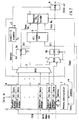
- the output unit shown in FIG. 2 has a buffer memory 1, a memory management unit 2, two multiplexers 3 and 4, two buffer memories 5a and 5b, two comparators 6 and 7, a further buffer memory 8 and a counter 9.
- a modulo-N counter is preferably used to assign the first type of mark, N being chosen to be so large that less than N / 2 numbers are assigned as first type of mark within a predetermined time. Because of the periodic appearance of all numbers, there must be a sufficiently large distance in both directions to be unambiguous. With the specified choice of N, all cells can be reconstructed unambiguously in their original order, which when the numbers are assigned are no further apart than the specified predetermined time. This time must then expediently be such that, apart from the permitted error rate, it is ensured that every cell runs through the last r memory locations of the buffer memory 1 within this time. As a rough guideline for the time to be specified, double the difference between the maximum and minimum duration between the award of the first type of stamp and the arrival at the exit unit can be assumed.
- VCI The second type of mark, identifies the affiliation of a cell to a specific virtual connection.
- the buffer memory 1 is divided into three parts, namely a shift register-like part, shift register, with memory locations 1 to d and a part operated in the manner of a FIFO memory, FIFO, which again consists of two parts with memory locations d + 1 to r and r + 1 to p is composed. At least the storage locations 1 to r must be individually accessible in such a way that their content can be read or that new content can be written into them.
- the dimensioning of the buffer memory ie the choice of the numerical values for d, r and p, must take place in the specific application.
- individual case examinations are essential.
- Cells arriving at the input of the output unit are first examined for whether they are cells to be output at the output or those that end in the output unit. These are on the one hand empty cells, on the other hand those which contain control signals for the output unit (or an input unit which is generally connected to it and which cannot otherwise be reached).
- the cells to be output are entered into the buffer memory 1 in such a way that they initially "fail” in the part operated in the manner of a FIFO memory except for the lowest free memory location. Whenever a cell is output at the output, all cells in the buffer memory move down by one space. If the last memory location of the FIFO memory, d + 1, is occupied, the cell contained therein is transferred to the first memory location of the shift register, d.
- memory location d + 1 is empty, then an empty cell must be written into memory location d.
- the length of stay of each cell can thus be derived, at least relative to every other cell, from its position in the buffer memory 1. The output from the buffer memory 1 will be described below.
- the memory management unit 2 is shown only very schematically in FIG. 2. It first has the task of ensuring the normal operation of the buffer memory 1 already described. This is done by applying addresses, address, write commands, W, and read commands, R. In addition, not shown in FIG. 2, information about the presence or absence of a cell to be written is required. Furthermore, the memory management unit 2 has the task of exchanging the content of the memory location addressed by the counter 9, Address, for the content of the intermediate memory 5b if a command, swap, is given for this.
- the content of one of the memory locations 2 to r of the buffer memory 1 can optionally be accessed by the multiplexer 3 and passed on to the buffer memory 5a.
- the memory location is selected using counter 9, address.
- the content of the intermediate store 5a is transferred to the intermediate store 5b by means of the multiplexer 4. It is not unusual for the same command, swap, to be written into and read from the buffer memory 5b and can be taken into account by the person skilled in the art by customary measures.
- the comparator 6 compares the marks of the second type, VCI, of those two cells that are currently stored in the intermediate memories 5a and 5b. Only if the two brands of the second type are the same, i.e. if the two cells belong to the same connection, the subsequent comparator is activated.
- the comparator 7 compares the marks of the first type, sequence number, of the two cells contained in the intermediate memories 5a and 5b. If the comparator 6 indicates that both cells belong to the same connection and it is determined that the cell contained in the buffer 5a is older than the cell contained in the buffer 5b, then a command, swap, is issued, by means of which the older cell is buffered 5b and the younger cell are taken over in their place in the buffer memory 1. As a result, the two cells are swapped.
- the content of the buffer memory 5b which was recognized in the previous cycle as the oldest cell belonging to a specific connection, is transferred to the buffer memory 8 and is available for output at its output, cells out.
- the content of the memory location 1 of the buffer memory 1 is transferred to the buffer memory 5b via the multiplexer 4. Subsequently, the memory locations 2 to r are placed on older cells (brands of the first type) Connection (brands of the second kind) examined.
- the content is transferred to the buffer 5a via the multiplexer 3 and compared by means of the comparators 6 and 7.
- the swap actions described above ensure that at the counter reading r of the counter 9 the oldest cell of the connection under consideration is actually stored in the buffer memory 5b and that all the younger cells of this connection are still or again contained in the buffer memory 1.
- the illustration of the output unit selected in FIG. 2 shows above all the functioning of the output unit.
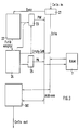
- the structure and management of the buffer memory with a part operated in the manner of a FIFO memory and a part operated in the manner of a shift register is clearly expressed in the illustration selected in FIG. 3.
- the distribution of the clocks, including the write and read commands, is not shown here.
- the buffer memory is implemented by a read-write memory (RAM), 1 '.
- the incoming cells are transferred via an input memory 21 to a data bus, data, to which the read-write memory 1 'is also connected.
- a write-in control 22 is activated by the input memory 21, busy when a cell to be written is present.
- an address PW is applied to the read-write memory 1 'via an address bus, Address, and the cell is written into it.
- the enrollment counter 23 is then incremented by the enrollment control 22.
- a read-out controller 24 uses a read-out counter 25 to indicate the address, PR, which corresponds to storage location 1.
- the readout counter 25 is incremented by the readout controller 24.
- the difference between the content PW of the write-in counter 23 and the content PR of the read-out counter 25 must always be at least equal to d. This is monitored by the write-in controller 22 and, if necessary, FIFO empty, is reported to the read-out controller 24, which then applies it to the data bus, data, an empty cell, and initiates the writing into the memory space indicated by the write-in counter 23 and then the write-in counter 23 incremented.
- the rest of the output unit is represented here by an access, comparator and output unit 100.
- the part of the buffer memory operated in the manner of a shift register does not necessarily have to form the end thereof. It can also be at the beginning or in the middle of the buffer memory.
- Typical examples of distribution services are conference calls and audio or television broadcasts.
- the associated cells represent a continuous signal stream. They arise at the transmitter at constant intervals and are not only required in the correct order at the receiver, but also again at the original constant intervals.
Landscapes
- Engineering & Computer Science (AREA)
- Computer Networks & Wireless Communication (AREA)
- Signal Processing (AREA)
- Data Exchanges In Wide-Area Networks (AREA)
- Electronic Switches (AREA)
- Input Circuits Of Receivers And Coupling Of Receivers And Audio Equipment (AREA)
- Use Of Switch Circuits For Exchanges And Methods Of Control Of Multiplex Exchanges (AREA)
Claims (3)
- Centrale de commutation ATM comportant une pluralité d'entrées (E), une pluralité de sorties (A) et un réseau de couplage (20), à travers lequel chaque cellule à commuter est guidée à partir d'une information de cheminement (VCI) sur un chemin déterminé, à connexion individuelle, caractérisée en ce que, entre le réseau de couplage (20) et chaque sortie, (A) une unité de sortie (30) comportant une mémoire-tampon (1, 1') est prévue pour mettre en mémoire-tampon des cellules à sortir, en ce que des moyens sont présents pour écrire chaque cellule dans la mémoire-tampon (1, 1') de l'unité de sortie (30) respective, après qu'elle a quitté le réseau de couplage (20) et pour déterminer la séquence de sortie des cellules depuis la mémoire-tampon (1, 1') au moyen de repères destinés à l'identification de la séquence (Sequence number).
- Centrale de commutation selon la revendication 1, caractérisée en ce que, entre chaque entrée (E) de la centrale de commutation et le réseau de couplage (20), est prévue une unité d'entrée (10), dans laquelle une information de cheminement (VCI) est ajoutée à chaque cellule.
- Centrale de commutation selon la revendication 1, caractérisée en ce que, entre chaque entrée (E) de la centrale de commutation et le réseau de couplage (20), est prévue une unité d'entrée (10), dans laquelle un repère, destiné à l'identification de la séquence (Sequence Number) est ajouté à chaque cellule.
Applications Claiming Priority (2)
| Application Number | Priority Date | Filing Date | Title |
|---|---|---|---|
| DE4008080 | 1990-03-14 | ||
| DE4008080A DE4008080A1 (de) | 1990-03-14 | 1990-03-14 | Atm-vermittlungsstelle |
Publications (3)
| Publication Number | Publication Date |
|---|---|
| EP0446586A2 EP0446586A2 (fr) | 1991-09-18 |
| EP0446586A3 EP0446586A3 (en) | 1992-04-29 |
| EP0446586B1 true EP0446586B1 (fr) | 1996-06-12 |
Family
ID=6402147
Family Applications (1)
| Application Number | Title | Priority Date | Filing Date |
|---|---|---|---|
| EP91101020A Expired - Lifetime EP0446586B1 (fr) | 1990-03-14 | 1991-01-26 | Central de commutation ATM |
Country Status (9)
| Country | Link |
|---|---|
| US (1) | US5319360A (fr) |
| EP (1) | EP0446586B1 (fr) |
| JP (1) | JPH0583283A (fr) |
| KR (1) | KR0157989B1 (fr) |
| AT (1) | ATE139397T1 (fr) |
| AU (1) | AU641480B2 (fr) |
| CA (1) | CA2037861C (fr) |
| DE (2) | DE4008080A1 (fr) |
| ES (1) | ES2090149T3 (fr) |
Families Citing this family (26)
| Publication number | Priority date | Publication date | Assignee | Title |
|---|---|---|---|---|
| FR2659819B1 (fr) * | 1990-03-14 | 1992-05-29 | Alcatel Nv | Reseau de commutation a trajets multiples et a autoacheminement pour la commutation de cellules a multiplexage temporel asynchrone. |
| EP0544034A1 (fr) * | 1991-11-28 | 1993-06-02 | Siemens Aktiengesellschaft | Procédé pour la reconstruction l'ordre des cellules de données |
| US5274642A (en) * | 1992-06-05 | 1993-12-28 | Indra Widjaja | Output buffered packet switch with a flexible buffer management scheme |
| ATE208975T1 (de) * | 1992-06-26 | 2001-11-15 | Siemens Ag | Verfahren zur behandlung der im kopfteil von im asynchronen transfermodus übertragenen nachrichtenzellen enthaltenden informationen |
| US5337313A (en) * | 1992-11-12 | 1994-08-09 | Motorola, Inc. | Method and apparatus for preserving packet squencing in a packet transmission system |
| EP0603424A1 (fr) * | 1992-12-21 | 1994-06-29 | Siemens Aktiengesellschaft | Procédé et circuit pour transmettre des cellules de communication par un dispositif de communication à ATM |
| EP0633678B1 (fr) * | 1993-06-29 | 2000-07-19 | Alcatel | Procédé et dispositif pour la remise en séquence |
| DE4343588A1 (de) * | 1993-12-21 | 1995-06-22 | Sel Alcatel Ag | Verfahren und Einrichtung zur zufälligen Auswahl einer von N gleichen Einheiten, sowie Koppelelement, Koppelnetz und Vermittlungsstelle damit |
| US5583863A (en) * | 1995-01-31 | 1996-12-10 | Bell Atlantic Network Services, Inc. | Full service network using asynchronous transfer mode multiplexing |
| US5908598A (en) * | 1995-08-14 | 1999-06-01 | Minnesota Mining And Manufacturing Company | Fibrous webs having enhanced electret properties |
| FI955814A7 (fi) * | 1995-12-01 | 1997-06-02 | Nokia Telecommunications Oy | Solujen osoitus ATM-järjestelmän soluvirrassa |
| US6542502B1 (en) * | 1996-01-26 | 2003-04-01 | International Business Machines Corporation | Multicasting using a wormhole routing switching element |
| KR100467708B1 (ko) * | 1996-12-21 | 2005-05-11 | 삼성전자주식회사 | 비동기전송모드교환시스템의셀처리장치및방법 |
| JP3434671B2 (ja) * | 1997-05-21 | 2003-08-11 | 沖電気工業株式会社 | Atmセル交換装置 |
| FI104672B (fi) * | 1997-07-14 | 2000-04-14 | Nokia Networks Oy | Kytkinjärjestely |
| KR100223300B1 (ko) * | 1997-09-10 | 1999-10-15 | 서평원 | 분산 제어와 난블로킹 교환 시스템 |
| US6373821B2 (en) * | 1998-02-20 | 2002-04-16 | Apple Computer, Inc. | Method for setting time stamp in SYT field of packet headers for IEEE-1394 devices |
| KR100279949B1 (ko) * | 1998-12-28 | 2001-02-01 | 윤종용 | 셀 재배열 버퍼 |
| JP2000295279A (ja) | 1999-04-02 | 2000-10-20 | Nec Corp | パケットスイッチ |
| US6757284B1 (en) * | 2000-03-07 | 2004-06-29 | Cisco Technology, Inc. | Method and apparatus for pipeline sorting of ordered streams of data items |
| US6747972B1 (en) * | 2000-03-07 | 2004-06-08 | Cisco Technology, Inc. | Method and apparatus for reducing the required size of sequence numbers used in resequencing packets |
| US6480491B1 (en) * | 2000-11-02 | 2002-11-12 | Intel Corporation | Latency management for a network |
| US7462103B2 (en) * | 2001-03-22 | 2008-12-09 | Igt | Gaming system for individual control of access to many devices with few wires |
| US7697570B2 (en) * | 2001-04-30 | 2010-04-13 | Huawei Technologies Co., Ltd. | Method based on backboard transmitting time division multiplexing circuit data and a bridge connector |
| US7525978B1 (en) * | 2005-04-15 | 2009-04-28 | Altera Corporation | Method and apparatus for scheduling in a packet buffering network |
| US7304498B2 (en) * | 2005-07-20 | 2007-12-04 | Altera Corporation | Clock circuitry for programmable logic devices |
Family Cites Families (7)
| Publication number | Priority date | Publication date | Assignee | Title |
|---|---|---|---|---|
| US4703475A (en) * | 1985-12-04 | 1987-10-27 | American Telephone And Telegraph Company At&T Bell Laboratories | Data communication method and apparatus using multiple physical data links |
| BE904100A (fr) * | 1986-01-24 | 1986-07-24 | Itt Ind Belgium | Systeme de commutation. |
| DE3742941A1 (de) * | 1987-12-18 | 1989-07-06 | Standard Elektrik Lorenz Ag | Einrichtungen zur paketvermittlung |
| JP2753254B2 (ja) * | 1988-04-06 | 1998-05-18 | 株式会社日立製作所 | パケツト交換システム |
| JP2860661B2 (ja) * | 1989-03-14 | 1999-02-24 | 国際電信電話 株式会社 | Atm交換機 |
| WO1991002419A1 (fr) * | 1989-08-09 | 1991-02-21 | Alcatel N.V. | Systeme de remise en sequence pour n×ud de commutation |
| JPH0382243A (ja) * | 1989-08-25 | 1991-04-08 | Nec Corp | セル時間順序回復装置 |
-
1990
- 1990-03-14 DE DE4008080A patent/DE4008080A1/de not_active Withdrawn
-
1991
- 1991-01-26 DE DE59107911T patent/DE59107911D1/de not_active Expired - Fee Related
- 1991-01-26 ES ES91101020T patent/ES2090149T3/es not_active Expired - Lifetime
- 1991-01-26 AT AT91101020T patent/ATE139397T1/de not_active IP Right Cessation
- 1991-01-26 EP EP91101020A patent/EP0446586B1/fr not_active Expired - Lifetime
- 1991-03-08 CA CA002037861A patent/CA2037861C/fr not_active Expired - Fee Related
- 1991-03-12 AU AU72836/91A patent/AU641480B2/en not_active Ceased
- 1991-03-12 KR KR1019910003914A patent/KR0157989B1/ko not_active Expired - Fee Related
- 1991-03-13 US US07/668,632 patent/US5319360A/en not_active Expired - Fee Related
- 1991-03-14 JP JP7468691A patent/JPH0583283A/ja active Pending
Also Published As
| Publication number | Publication date |
|---|---|
| KR910017805A (ko) | 1991-11-05 |
| CA2037861C (fr) | 1996-05-28 |
| AU641480B2 (en) | 1993-09-23 |
| EP0446586A2 (fr) | 1991-09-18 |
| DE59107911D1 (de) | 1996-07-18 |
| KR0157989B1 (ko) | 1999-02-18 |
| EP0446586A3 (en) | 1992-04-29 |
| DE4008080A1 (de) | 1991-09-19 |
| JPH0583283A (ja) | 1993-04-02 |
| CA2037861A1 (fr) | 1991-09-15 |
| ES2090149T3 (es) | 1996-10-16 |
| ATE139397T1 (de) | 1996-06-15 |
| AU7283691A (en) | 1991-09-19 |
| US5319360A (en) | 1994-06-07 |
Similar Documents
| Publication | Publication Date | Title |
|---|---|---|
| EP0446586B1 (fr) | Central de commutation ATM | |
| EP0435046B1 (fr) | Méthode pour le rétablissement de la séquence des cellules originelles, notamment pour un commutateur ATM, ainsi qu'unité de sortie pour celui-ci | |
| EP0446589B1 (fr) | Commutateur ATM avec capacité de duplication | |
| DE69031300T2 (de) | Schnelles Paketvermittlungsnetzwerksystem des ATM-Typs (asynchronous transfer mode) mit einer Einheit für die Zuteilung von Zeitschlitzen | |
| DE3752370T2 (de) | Vermittlungssystem | |
| DE69112746T2 (de) | Datenpufferungssystem mit einem Pufferspeicher der Datenblöcke mit fester oder veränderlicher Länge speichert. | |
| DE3214189C2 (fr) | ||
| DE3875993T2 (de) | Vermittlungssystem fuer hybride zeitmultiplexe. | |
| DE3137627C1 (de) | Anordnung zur schnellen Nachrichtenuebertragung zwischen Rechnern | |
| DE2249371C2 (de) | Zeitvielfachvermittlungsanlage | |
| DE2061576A1 (de) | Speicheranordnung | |
| EP0024708B1 (fr) | Multiple de canaux temporels pour un système à multiplexage temporel pour la commutation de signaux numériques, en particulier de messages à modulation en delta | |
| EP0025577B1 (fr) | Circuit pour la compensation des différences de phase entre l'horloge de voie d'une ligne à division temporelle MIC connectée à un central MIC et l'horloge locale de ce central | |
| EP0651536A2 (fr) | Procédé pour rétablir la séquence originelle de cellules ATM | |
| EP0004307B1 (fr) | Procédé pour la réalisation de connexions en conférence dans un système de commutation temporelle MIC | |
| DE2155102A1 (de) | Elektronisches Schaltsystem | |
| EP0566961A2 (fr) | Procédé et circuit pour faire respecter le débit de transmission préaccordé dans un dispositif de commutation ATM | |
| DE3856504T2 (de) | Zeitmultiplex-Schaltnetz mit Vielfachzugriff und Zeitschalter | |
| DE69020813T2 (de) | Arbitrierungsverfahren und Vorrichtung für Sendezugriff zu einem Übertragungsmedium eines verteilten Vermittlungsnetzes. | |
| DE2312461A1 (de) | Schaltungsanordnung zur verbindung einer datenverarbeitungseinheit mit einer vielzahl von uebertragungsleitungen | |
| DE2517525A1 (de) | Signalisierungsidentifizierer | |
| EP0173274B1 (fr) | Méthode et montage pour la réalisation et la maintenance d'une liaison à division temporelle à large bande | |
| EP0414950B1 (fr) | Méthode de commutation des informations transmises distributivement sur plusieurs tranches de temps | |
| EP0579845A1 (fr) | Réseau de couplages à étages parallèles à l'entrée pour carteaux numériques | |
| EP0531772A2 (fr) | Dispositif et appareil pour convertir la structure des données de communication dans un système de commutation de paquets |
Legal Events
| Date | Code | Title | Description |
|---|---|---|---|
| PUAI | Public reference made under article 153(3) epc to a published international application that has entered the european phase |
Free format text: ORIGINAL CODE: 0009012 |
|
| AK | Designated contracting states |
Kind code of ref document: A2 Designated state(s): AT BE CH DE ES FR GB IT LI NL SE |
|
| PUAL | Search report despatched |
Free format text: ORIGINAL CODE: 0009013 |
|
| AK | Designated contracting states |
Kind code of ref document: A3 Designated state(s): AT BE CH DE ES FR GB IT LI NL SE |
|
| 17P | Request for examination filed |
Effective date: 19920411 |
|
| RAP3 | Party data changed (applicant data changed or rights of an application transferred) |
Owner name: ALCATEL N.V. Owner name: ALCATEL SEL AKTIENGESELLSCHAFT |
|
| 17Q | First examination report despatched |
Effective date: 19940607 |
|
| GRAA | (expected) grant |
Free format text: ORIGINAL CODE: 0009210 |
|
| AK | Designated contracting states |
Kind code of ref document: B1 Designated state(s): AT BE CH DE ES FR GB IT LI NL SE |
|
| REF | Corresponds to: |
Ref document number: 139397 Country of ref document: AT Date of ref document: 19960615 Kind code of ref document: T |
|
| REG | Reference to a national code |
Ref country code: CH Ref legal event code: NV Representative=s name: JUERG ULRICH C/O ALCATEL STR AG |
|
| REF | Corresponds to: |
Ref document number: 59107911 Country of ref document: DE Date of ref document: 19960718 |
|
| GBT | Gb: translation of ep patent filed (gb section 77(6)(a)/1977) |
Effective date: 19960726 |
|
| ITF | It: translation for a ep patent filed | ||
| ET | Fr: translation filed | ||
| REG | Reference to a national code |
Ref country code: ES Ref legal event code: FG2A Ref document number: 2090149 Country of ref document: ES Kind code of ref document: T3 |
|
| REG | Reference to a national code |
Ref country code: ES Ref legal event code: FG2A Ref document number: 2090149 Country of ref document: ES Kind code of ref document: T3 |
|
| PLBE | No opposition filed within time limit |
Free format text: ORIGINAL CODE: 0009261 |
|
| STAA | Information on the status of an ep patent application or granted ep patent |
Free format text: STATUS: NO OPPOSITION FILED WITHIN TIME LIMIT |
|
| 26N | No opposition filed | ||
| PGFP | Annual fee paid to national office [announced via postgrant information from national office to epo] |
Ref country code: GB Payment date: 20011214 Year of fee payment: 12 |
|
| PGFP | Annual fee paid to national office [announced via postgrant information from national office to epo] |
Ref country code: DE Payment date: 20011217 Year of fee payment: 12 Ref country code: CH Payment date: 20011217 Year of fee payment: 12 |
|
| PGFP | Annual fee paid to national office [announced via postgrant information from national office to epo] |
Ref country code: FR Payment date: 20011226 Year of fee payment: 12 |
|
| PGFP | Annual fee paid to national office [announced via postgrant information from national office to epo] |
Ref country code: NL Payment date: 20011227 Year of fee payment: 12 |
|
| PGFP | Annual fee paid to national office [announced via postgrant information from national office to epo] |
Ref country code: AT Payment date: 20011228 Year of fee payment: 12 |
|
| REG | Reference to a national code |
Ref country code: GB Ref legal event code: IF02 |
|
| PGFP | Annual fee paid to national office [announced via postgrant information from national office to epo] |
Ref country code: SE Payment date: 20020102 Year of fee payment: 12 |
|
| PGFP | Annual fee paid to national office [announced via postgrant information from national office to epo] |
Ref country code: ES Payment date: 20020118 Year of fee payment: 12 |
|
| PGFP | Annual fee paid to national office [announced via postgrant information from national office to epo] |
Ref country code: BE Payment date: 20020220 Year of fee payment: 12 |
|
| PG25 | Lapsed in a contracting state [announced via postgrant information from national office to epo] |
Ref country code: GB Free format text: LAPSE BECAUSE OF NON-PAYMENT OF DUE FEES Effective date: 20030126 Ref country code: AT Free format text: LAPSE BECAUSE OF NON-PAYMENT OF DUE FEES Effective date: 20030126 |
|
| PG25 | Lapsed in a contracting state [announced via postgrant information from national office to epo] |
Ref country code: SE Free format text: LAPSE BECAUSE OF NON-PAYMENT OF DUE FEES Effective date: 20030127 Ref country code: ES Free format text: LAPSE BECAUSE OF NON-PAYMENT OF DUE FEES Effective date: 20030127 |
|
| PG25 | Lapsed in a contracting state [announced via postgrant information from national office to epo] |
Ref country code: LI Free format text: LAPSE BECAUSE OF NON-PAYMENT OF DUE FEES Effective date: 20030131 Ref country code: CH Free format text: LAPSE BECAUSE OF NON-PAYMENT OF DUE FEES Effective date: 20030131 Ref country code: BE Free format text: LAPSE BECAUSE OF NON-PAYMENT OF DUE FEES Effective date: 20030131 |
|
| PG25 | Lapsed in a contracting state [announced via postgrant information from national office to epo] |
Ref country code: NL Free format text: LAPSE BECAUSE OF NON-PAYMENT OF DUE FEES Effective date: 20030801 Ref country code: DE Free format text: LAPSE BECAUSE OF NON-PAYMENT OF DUE FEES Effective date: 20030801 |
|
| EUG | Se: european patent has lapsed | ||
| REG | Reference to a national code |
Ref country code: CH Ref legal event code: PL |
|
| GBPC | Gb: european patent ceased through non-payment of renewal fee | ||
| PG25 | Lapsed in a contracting state [announced via postgrant information from national office to epo] |
Ref country code: FR Free format text: LAPSE BECAUSE OF NON-PAYMENT OF DUE FEES Effective date: 20030930 |
|
| NLV4 | Nl: lapsed or anulled due to non-payment of the annual fee |
Effective date: 20030801 |
|
| REG | Reference to a national code |
Ref country code: FR Ref legal event code: ST |
|
| REG | Reference to a national code |
Ref country code: ES Ref legal event code: FD2A Effective date: 20030127 |
|
| PG25 | Lapsed in a contracting state [announced via postgrant information from national office to epo] |
Ref country code: IT Free format text: LAPSE BECAUSE OF NON-PAYMENT OF DUE FEES;WARNING: LAPSES OF ITALIAN PATENTS WITH EFFECTIVE DATE BEFORE 2007 MAY HAVE OCCURRED AT ANY TIME BEFORE 2007. THE CORRECT EFFECTIVE DATE MAY BE DIFFERENT FROM THE ONE RECORDED. Effective date: 20050126 |