EP0446711B1 - Module optique comportant un récipient et procédé pour la fabrication de celui-ci - Google Patents
Module optique comportant un récipient et procédé pour la fabrication de celui-ci Download PDFInfo
- Publication number
- EP0446711B1 EP0446711B1 EP91102962A EP91102962A EP0446711B1 EP 0446711 B1 EP0446711 B1 EP 0446711B1 EP 91102962 A EP91102962 A EP 91102962A EP 91102962 A EP91102962 A EP 91102962A EP 0446711 B1 EP0446711 B1 EP 0446711B1
- Authority
- EP
- European Patent Office
- Prior art keywords
- optical
- module
- sub
- receptacle
- core
- Prior art date
- Legal status (The legal status is an assumption and is not a legal conclusion. Google has not performed a legal analysis and makes no representation as to the accuracy of the status listed.)
- Expired - Lifetime
Links
Images


Classifications
-
- G—PHYSICS
- G02—OPTICS
- G02B—OPTICAL ELEMENTS, SYSTEMS OR APPARATUS
- G02B6/00—Light guides; Structural details of arrangements comprising light guides and other optical elements, e.g. couplings
- G02B6/24—Coupling light guides
- G02B6/42—Coupling light guides with opto-electronic elements
- G02B6/4292—Coupling light guides with opto-electronic elements the light guide being disconnectable from the opto-electronic element, e.g. mutually self aligning arrangements
-
- B—PERFORMING OPERATIONS; TRANSPORTING
- B29—WORKING OF PLASTICS; WORKING OF SUBSTANCES IN A PLASTIC STATE IN GENERAL
- B29C—SHAPING OR JOINING OF PLASTICS; SHAPING OF MATERIAL IN A PLASTIC STATE, NOT OTHERWISE PROVIDED FOR; AFTER-TREATMENT OF THE SHAPED PRODUCTS, e.g. REPAIRING
- B29C70/00—Shaping composites, i.e. plastics material comprising reinforcements, fillers or preformed parts, e.g. inserts
- B29C70/68—Shaping composites, i.e. plastics material comprising reinforcements, fillers or preformed parts, e.g. inserts by incorporating or moulding on preformed parts, e.g. inserts or layers, e.g. foam blocks
-
- G—PHYSICS
- G02—OPTICS
- G02B—OPTICAL ELEMENTS, SYSTEMS OR APPARATUS
- G02B6/00—Light guides; Structural details of arrangements comprising light guides and other optical elements, e.g. couplings
- G02B6/24—Coupling light guides
- G02B6/42—Coupling light guides with opto-electronic elements
- G02B6/4201—Packages, e.g. shape, construction, internal or external details
- G02B6/4246—Bidirectionally operating package structures
-
- B—PERFORMING OPERATIONS; TRANSPORTING
- B29—WORKING OF PLASTICS; WORKING OF SUBSTANCES IN A PLASTIC STATE IN GENERAL
- B29L—INDEXING SCHEME ASSOCIATED WITH SUBCLASS B29C, RELATING TO PARTICULAR ARTICLES
- B29L2031/00—Other particular articles
- B29L2031/34—Electrical apparatus, e.g. sparking plugs or parts thereof
- B29L2031/3406—Components, e.g. resistors
-
- H—ELECTRICITY
- H10—SEMICONDUCTOR DEVICES; ELECTRIC SOLID-STATE DEVICES NOT OTHERWISE PROVIDED FOR
- H10W—GENERIC PACKAGES, INTERCONNECTIONS, CONNECTORS OR OTHER CONSTRUCTIONAL DETAILS OF DEVICES COVERED BY CLASS H10
- H10W90/00—Package configurations
- H10W90/701—Package configurations characterised by the relative positions of pads or connectors relative to package parts
- H10W90/751—Package configurations characterised by the relative positions of pads or connectors relative to package parts of bond wires
- H10W90/754—Package configurations characterised by the relative positions of pads or connectors relative to package parts of bond wires between a chip and a stacked insulating package substrate, interposer or RDL
Definitions
- the present invention relates to an optical module for use in an optical communication system using light as an information transmitting medium, such as data link, optical LAN, and so on, and a method of producing the same.
- the optical module comprises at least one sub-module having at least one optical connector socket, which is fitted in a ferrule of an optical plug and to which an electro-optical element (light emitting element or light receiving element) is fixed, and at least one receptacle fitted to the optical plug to prevent the plug from falling off.
- an optical module having a plurality of optical connector sockets (a multi-core optical module) has been produced in such a manner that after single-core optical sub-modules each for optically coupling an electro-optical element and an optical fiber connector ferrule with each other have been produced, plural ones of the thus produced single-core optical sub-modules are combined.
- Those single-core optical sub-modules may be classified into two, one being a transmitting module using a light emitting element such as a semiconductor laser as an optical operation element, the other being a receiving module using a light receiving element such as a pin photo-diode as an optical operation element.
- a method of manufacturing a single transmitter module for a fibre optic link is described in US-A-4,410,469.
- the light emitting element is already formed together with the necessary circuitry as a single module which is clamped between a pair of rod-shaped first dies which have a common central axis for defining an optical path of the module.
- the clamped module is housed in a cavity defined by a pair of second dies. Transfer molding then takes place to complete the casing for the transmitter module.
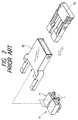
- Fig. 1 shows an example of the structure of a conventional single-core optical sub-module.
- an electro-optical element (light emitting or light receiving element) 2 is fixed by an adhesive or the like to an optical connector socket 1 to be fitted in a ferrule (not shown) which is fixed to an end portion of an optical fiber (not shown), after adjusting its optical axis.
- the optical connector socket 1 to which the electro-optical element 2 is fixed is fixed to a ceramic package 3 by an adhesive or the like.
- To the ceramic package 3, in addition to the optical connector socket 1, fixed is a substrate 6 supporting an electronic circuit portion constituted by electronic circuit parts such as a bare chip IC 5 and so on.
- the bare chip IC 5 and the like mounted on the substrate 6 together with wires connecting them to a wiring pattern on the substrate 6 are sealed by a lid 7.
- lead pins 8 constituted by inner leads 8a and outer leads 8b respectively erected from the inner and outer sides of the package.
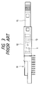
- a plurality of single-core optical sub-modules 11 constituted as described above are assembled to a receptacle 12 as shown in Figs. 2 and 3 to thereby form a conventional multi-core optical module.
- a multi-core optical module is attached/detached to/from a multi-core plug having a plurality of ferrules 13 in the receptacle 12 in practical use, and, therefore, a high positioning accuracy is required in attaching the single-core optical sub-modules 11 to the receptacle 12.
- the present invention achieves its object by providing an optical module comprising the features set out in claim 1.
- the present invention also claims an apparatus for producing the optical module as claimed in claim 7, as well as a method for producing the optical module comprising the steps set out in claim 8.
- the optical module according to the present invention is formed by using a mold die for resin molding.
- the mold die includes a core for forming the opening portion of the receptacle, the core having at least one end portion having a cavity formed in the core adapted to receive the end portion of the optical connector socket of the sub-module.
- the relative positional accuracy between the opening portion of the receptacle and the optical connector can be improved since the accuracy is determined by the dimensional accuracy realized in the mold die.
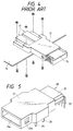
- Fig. 5 shows a multi-core optical module according to the first embodiment of the present invention when applied to a two-core light transmitting/receiving module.
- a two-core optical sub-module 20 having two optical connector sockets is formed so as to be integrally held by a receptacle 21 of mold resin.
- the parts constituting the two-core optical sub-module 20, such as optical connector sockets 22, lead pins 23 etc., are integrally held by a molded resin member 25 to thereby form the two-core optical sub-module 20.
- the optical connector sockets 22 are held by the molded resin member 25 so that their end portions at which optical fiber ferrules (not shown) are to be received, are projected outside, and the two-core optical sub-module 20 is integrally held by the receptacle 21 so that the end portions of the optical connector sockets 22 are enveloped in the receptacle 21.
- a light emitting element is fixed to one of the two optical connector sockets and a light receiving element is fixed to the other optical connector socket.
- the multi-core optical sub-module may have only light emitting elements or only light receiving elements.
- an opening portion 21a is formed so as to open at the side thereof opposite to the side at which the two-core optical sub-module 20 is held. End portions of two optical fiber ferrules are held by an optical plug which is to be fitted into the opening portion 21a. Therefore, when the optical plug is inserted and fitted into the opening portion 21a, the optical fiber ferrule end portions are received by the end portions of the optical connectors 22 enveloped by the receptacle 21 so that the optical fiber ferrule end portions are optically coupled with the electro-optical elements respectively fixed to the optical connector sockets 22.
- Latch holes 21b are opened in the portions aside the opening portion 21a, and when the optical plug is fitted into the opening portion 21a, elastic projections formed in the side portions of the optical plug are engaged thereto, so that the optical plug is held so as not to be detached from the receptacle 21.
- integrally held are stud pins 26 for fixing the receptacle 21 to a printed circuit board or the like.
- Fig. 6 shows a state of the constituent parts such as optical connector sockets 22 constituting the two-core optical sub-module 20 after resin molding.
- the above-mentioned two-core optical module is produced in such a manner that the two-core optical sub-module 20 is produced and then the receptacle 21 is produced with the two-core optical sub-module 20 as an insert part.
- the two-core optical sub-module 20 is produced, for example, by attaching constituent parts of the two-core optical sub-module 20 to a lead frame 30, integrally holding the entire except for end portions of the optical connector sockets 22 and parts of the lead pins 23 as outer leads through molding resin to thereby form the two-core optical sub-module 20 as shown in Fig. 6, and cutting off unnecessary parts of the lead frame 30 through a press machine or the like.
- the thus produced two-core optical sub-module 20 is fitted as an insert part into a mold die for forming a receptacle which will be described later, molding resin is poured into this mold die for molding a receptacle to thereby form the receptacle 21 integrally holding the two-core optical sub-module 20, and a two-core light transmitting/receiving module as shown in Fig. 5 is completed.
- Fig. 7 shows an example of the mold die for molding the receptacle.
- this mold die is constituted by upper and lower molds 40 and 41, there are provided a core 42 for forming the opening portion, and two cores 43 for forming latch holes.
- recess portions 40a and 41a for forming the outer shape of the receptacle 21, core holding portions 40b and 41b into which the core 42 is fitted slidably, core holding portions 40c and 41c into which the cores 43 are fitted slidably, and recess portions 40d and 41d for receiving the two-core optical sub-module 20.
- the recess portions 40d and 41d are formed so as to be continuous to the recess portions 40a and 41a.
- the core 42 is fitted into the core holding portions 40b and 41b so as to be held between the upper and lower molds 40 and 41, and the core projects into a cavity formed by the recess portions 40a and 41a of the upper and lower molds to thereby form the inner shape of the receptacle 21. Further, as shown in Fig.
- a fitting recess portion 42a is formed in a top end portion of the core 42 projecting into the cavity, so that the fitting recess portion 42a is tightly fitted with the two-core optical sub-module 20 in the state that the end portions of the optical connector sockets 22 provided in the two-core optical sub-module 20 are enveloped.
- the cores 43 are fitted into the core holding portions 40c and 41c so as to be engaged with the recess portions 42b formed in the side portions of the core 42 to thereby form the latch holes 21b of the receptacle 21.
- the stud pins 26 and the two-core optical sub-module 20 as insert parts are fitted into such a mold die for forming a receptacle, and molding resin is poured into the mold die, to thereby form the receptacle 21 to integrally hold the two-core optical sub-module 20. Accordingly, it is possible to produce a two-core light transmitting/receiving module with a high dimensional accuracy.
- the lead pins 23 provided in the two-core optical sub-module 20 are bent into a predetermined shape after the resin molding. Consequently, such a two-core light transmitting/receiving module as shown in Fig. 5 is completed.
- the fitting recess portion 42a in which the two-core optical sub-module 20 is to be tightly fitted is formed in the core 42 so as to make this core 42 have a function to determine the relative positional relationship between the opening portion 21a of the receptacle and the optical connector sockets 22. Therefore, the dimensional accuracy of the relative positional relationship between the opening portion 21a of the receptacle and the optical connector sockets 22 is determined by the dimensional accuracy of the fitting recess portion 42a and the outer dimensional accuracy of two-core optical sub-module 20.
- the two-core optical sub- module 20 having a high outer dimensional accuracy can be obtained in the above-mentioned manner, after all, the dimensional accuracy of the above relative positional relationship can be determined by the dimensional accuracy in producing the core. Accordingly, if the sizes M and N of the fitting recess portion 42a shown in Fig. 8(a) are made close to the outer size of the two-core optical sub-module 20, it is possible to improve the relative positional accuracy between the receptacle opening portion 21a and the optical connector sockets 22 provided in the two-core optical sub-module 20. In addition, as shown in Fig.
- the technical level of producing the mold die including the core 42 and so on has reached the degree which makes it possible to realize a very high dimensional accuracy, so that the dimensional accuracy required in the relative positional relationship between the receptacle 21 and the optical connector sockets 22 is sufficiently satisfied. Therefore, without using such an aligning tool as used conventionally, it is possible to mass-produce two-core light transmitting/receiving modules with a high dimensional accuracy in their finished state with superior reproducibility, through the above-mentioned resin molding.
- the conventional troublesome working of alignment with an expensive aligning tool is unnecessary when a multi-core optical module is mounted on a fixed object such as a printed circuit board. That is, it is possible to easily mount the multi-core optical module as it is on the fixed object such as a printed circuit board.
- the first embodiment of the present invention it is possible to simplify the process of assembling the constituent parts. Moreover, since the configuration is made such that the constituent parts are integrally held by inexpensive molding resin which is to be formed by transfer molding or the like, it is possible to form a number of multi-core optical modules at the same time, resulting in a superior mass productivity. It is therefore possible to provide a plurality of multi-core optical modules at a low cost.
- the assembling positional accuracy of the optical connector sockets relative to each other or relative to the multi-core optical sub-module is determined by the high dimensional accuracy realized in the mold die for molding the multi-core optical sub-module, and the relative positional accuracy between the receptacle and the optical connector sockets is determined by the high dimensional accuracy realized in the mold die (including the core) for molding the receptacle. Therefore, without using such an aligning tool as used conventionally, it is possible to mass-produce multi-core optical modules with a high dimensional accuracy in their finished state with a superior reproducibility, through resin molding.
- Fig. 9 is a perspective view illustrating a multi-core optical module according to the second embodiment of the present invention applied to a two-core light transmitting/receiving module
- Fig. 10 is an exploded view illustrating a mold die used to form the multi-core optical module.
- two single-core optical sub-modules 120 are integrally held by a receptacle 121 composed of molding resin.
- each of the single-core optical sub-modules 120 is formed by integrally holding parts constituting the single-core optical sub-module 120 such as an optical connector socket 122 and lead pins 123 by a molded resin member 125.
- Each optical connector socket 122 is held by the molded resin member 125 in such a manner that the socket 122 is projected at its one end by which an end of an optical fiber ferrule (not-shown) is received.
- the two single-core optical sub-modules 120 are held by the receptacle 121 in such a manner that the respective ends of the optical connector sockets are included in the receptacle 121.
- one of the two single-core optical sub-modules 120 is provided with a light emitting element for light transmission, and the other one is provided with a light receiving element for light reception.
- all single-core optical sub-modules may be for light transmission or for light reception.
- an opening portion 121a is formed so as to open at the side opposite to the side at which the receptacle holds the single-core optical sub-modules 120.
- the respective ends of two optical fiber ferrules are held by an optical plug which is to be fitted into the opening portion 121a, so that if the optical plug is fittingly inserted into the opening portion 121a, the respective end portions of the two optical fiber ferrules are received by the respective ends of optical connector sockets enveloped in the receptacle 121 so as to be optically coupled with electro-optical elements fixed to the optical connector sockets.
- Latch holes 121b are opened in the side portions aside the opening portion 121a, so that when the optical plug is fitted into the opening portion 121a, elastic projections formed at side portions of the optical plug are engaged with those latch holes 121b to thereby prevent the optical plug from coming off from the receptacle 121. Further, stud pins 126 for fixing the receptacle 121 to a printed circuit board or the like are integrally held in the receptacle 121.
- the illustrated mold die for resin molding the receptacle 121 is constituted by an upper mold 130, a lower mold 131, a core 132 for forming the opening portion, and two cores 133 for forming the latch holes.
- the illustrated mold die for resin molding the receptacle 121 is constituted by an upper mold 130, a lower mold 131, a core 132 for forming the opening portion, and two cores 133 for forming the latch holes.
- the upper and lower molds 130 and 131 there are formed not only recess portions 130a and 131a for forming an outer shape of the receptacle 121, but also core holding portions 130b and 131b for slidably mounting the core 132 therein, and core holding portions 130c and 131c for slidably mounting the cores 133.
- recess portions 130d and 131d in two pairs for receiving the single-core optical sub-modules 120 are formed respectively.
- the pairs of recess portions 130d and 131d are formed so as to continue with the recess portions 130a and 130b respectively.
- the core 132 is mounted in the core holding portions 130b and 131b so as to be held between the upper and lower molds 130 and 131 and so as to project into a cavity formed by the respective recess portions 130a and 131a of the upper and lower molds 130 and 131 to thereby form an inner shape of the receptacle 121.
- fitting holes 132a are formed as shown in Fig.
- the cores 133 are mounted in the core holding portions 130c and 131c and engaged with recess portions 132b formed in the side portions of the core 132 to thereby form the latch holes 121b of the receptacle 121 respectively.
- the single-core optical sub-modules 120 are repared, the respective ends of the optical connector sockets 122 provided in the single-core optical sub-modules 120 are fit into the fitting holes 132a of the core 132 respectively, and then the thus assembled core 132 and single-core optical sub-modules 120 are attached to the core holding portions 130b and 131b and the recess portions 130d and 131d of the upper and lower molds respectively.
- the stud pins 126 are attached to the lower mold 131.
- the cores 133 for forming latch holes are mounted in the core holding portions 130c and 131c respectively, and the inner end portions of the cores 133 are engaged with the respective recess portions 132b of the core 132. Thereafter, plasticized molding resin is injected into the cavity formed by the respective recess portions 130a and 131a of the upper and lower molds to thereby form the receptacle 121 which is holding the two single-core optical sub-modules 120 integrally.
- the lead pins 123 provided on each of the single-core optical sub-modules 120 are bent into a predetermined shape to thereby obtain a two-core light transmitting/receiving optical module having such a structure that the receptacle 121 is holding the two single-core optical sub-modules 120 integrally as shown in Fig. 9.
- the single-core optical sub-modules 120 together with the core 132 are attached to the upper and lower molds 130 and 131 after making the core 132 hold the respective ends of the optical connector sockets 122 provided in the respective single-core optical sub-modules 120.
- the single-core optical sub-modules 120 may be attached to the recess portions 130d and 131d of the respective upper and lower molds 130 and 131 in advance and thereafter the respective ends of the optical connector sockets 122 provided in the single-core optical sub-modules 120 may be fitted in the fitting holes 132a of the core 132 respectively.
- the molding resin to be injected into the mold die it is preferable to use poly-phenylene-sulfide (PPS) or epoxy resin having a high dimensional stability.
- PPS poly-phenylene-sulfide
- epoxy resin having a high dimensional stability.
- the two fitting holes 132a are formed in the core 132 as hold portions for holding the respective end portions of the optical connectors 122 provided in the respective single-core optical sub-modules 120 so as to make the core 132 have a function of determining the relative positional relationship between the optical connector sockets 122 and the relative positional relationship between the opening portion 121a of the receptacle 121 and each of the optical connector sockets 122.
- the dimensional accuracy related to the relative positional relationship between the optical connector sockets 122 and the relative positional relationship between the opening portion 121a of the receptacle 121 and each of the optical connector sockets 122 are determined. Since it has been possible to obtain optical connector sockets 122 having high accuracy in size conventionally, after all, the dimensional accuracy on those relative positional relationships depends on the dimensional accuracy in producing the core 132.
- the technical level of producing mold dies for resin molding including the core 132 and so on has reached the degree possible to realize a very high dimensional accuracy so as to satisfy the dimensional accuracy required in the relative positional relationship between the optical connector sockets 122 and the relative positional relationship between each of the optical connector sockets 122 and the receptacle 121. Therefore, without using such an aligning tool as used conventionally, it is possible to mass produce two-core light transmitting/receiving modules with a high dimensional accuracy in their finished state having a superior reproducibility by the above-mentioned resin molding.
- a conventional troublesome work of alignment with an expensive aligning tool is unnecessary when a multi-core optical module is mounted on a fixed object such as a printed circuit board, and it is therefore possible to easily mount the multi-core optical module as it is on the fixed object such as a printed circuit board.
- the optical connector sockets 122 are positioned with reference to their outer diameter center axial lines.
- single-core optical sub-modules used are not conventional single-core optical sub-modules each obtained by successively assembling constituent parts such as an optical connector on a package of ceramics or the like as shown in Fig. 1, but single-core optical sub-modules in which the constituent parts such as an optical connector socket are held integrally in molding resin. This is because if the assembling accuracy of the optical connector sockets 122 relative to the outer size of the single-core optical sub-modules 120 as a whole is low, it is necessary to form the recess portions 130d and 131d receiving single-core optical sub-modules in a mold die more largely in view of the assembling tolerance.
- single-core optical sub-modules in each of which the constituent parts such as an optical connector socket are held integrally in molding resin.
- the single-core optical sub-modules are formed while the end portions of the optical connector sockets are tightly held by the mold die for forming the single-core optical sub-modules. Accordingly, it is possible to obtain single-core optical sub-module with a high positional accuracy in assembling the optical connector sockets therein correspondingly to the high dimensional accuracy realized in the mold die.
- the dimensional accuracy between a plurality of optical connector sockets held integrally in a receptacle and the relative position accuracy of an opening portion of the receptacle and each of the optical connector sockets are determined by the high dimensional accuracy realized in a mold die (including a core) used in forming the receptacle.
- a receptacle 121 integrally holds a single-core optical sub-module 120 to envelope the entire portion of an optical connector socket (third embodiment).
- a receptacle 121 integrally holds a single-core optical sub-module to envelope a portion of the optical connector socket 122 (fourth embodiment).
- a latch projection 121c is provided instead of a latch hole 121b in Fig. 12.
- FIG. 14 shows an optical module according to a fifth embodiment of the present invention in which a plurality of receptacles 121 integrally hold a multi-core optical sub-module 20 such that each of the receptacles envelopes a portion of each of optical connector sockets 22.
Landscapes
- Physics & Mathematics (AREA)
- General Physics & Mathematics (AREA)
- Optics & Photonics (AREA)
- Chemical & Material Sciences (AREA)
- Engineering & Computer Science (AREA)
- Composite Materials (AREA)
- Mechanical Engineering (AREA)
- Optical Couplings Of Light Guides (AREA)
Claims (17)
- Module optique comprenant au moins un sous-module optique (20) possédant au moins une fiche femelle allongée de connecteur (22) se projetant du sous-module pour recevoir à coulissement une partie d'extrémité d'une bague de connecteur de fibre optique de façon à coupler optiquement ladite partie d'extrémité de ladite bague de fibre optique avec un élément électro-optique dans le sous-module,
module caractérisé par :- une pièce en résine moulée (25) entourant ledit sous-module (20) à l'exception de la partie d'extrémité de ladite fiche femelle de connecteur optique (22); et- au moins un boîtier (21) directement moulé sur ledit sous-module et encerclant la partie d'extrémité de ladite fiche femelle de connecteur de façon à former une unité intégrale avec ledit sous-module optique (20), ledit boîtier ayant une partie d'ouverture (21a) pour une adaptation avec une fiche mâle optique maintenant ladite bague afin de permettre ainsi à la bague d'être reçue par ladite fiche femelle de connecteur optique. - Module optique selon la revendication 1, dans lequel ledit module optique comprend un seul sous-module optique (20) possédant une pluralité de fiches femelles de connecteur (22) se projetant du moulage en résine et dans lequel ledit boîtier moulé enveloppe toutes les fiches femelles de connecteur.
- Module optique selon la revendication 1, dans lequel ledit module optique comprend une pluralité de sous-modules optiques moulés (120) possédant chacun une seule fiche femelle de connecteur (122) et dans lequel ledit boîtier moulé (121) enveloppe toutes les fiches femelles de connecteur optique.
- Module optique selon la revendication 1, dans lequel ledit module optique comprend un seul sous-module optique moulé (120) possédant une seule fiche femelle de connecteur et dans lequel ledit boîtier enveloppe complètement tout le sous-module.
- Module optique selon la revendication 1, dans lequel ledit module optique comprend un seul sous-module moulé possédant une seule fiche femelle de connecteur et dans lequel ledit boîtier enveloppe la partie d'extrémité de ladite fiche femelle de connecteur.
- Module optique selon la revendication 1, dans lequel ledit module optique comprend une pluralité de socles moulés et un seul sous-module optique moulé possédant une pluralité de fiches femelles de connecteur et dans lequel lesdits socles sont moulés sur ledit sous-module optique de telle façon que chacun desdits socles enveloppe une partie d'extrémité de chacune desdites fiches femelles de connecteur.
- Dispositif pour la production d'un module optique selon la revendication 1, comprenant une matrice de moulage (40, 41) pour le moulage en résine dudit boîtier, dispositif dans lequel ladite matrice de moulage comprend un noyau (42) placé à l'intérieur du moule pour la formation de ladite partie d'extrémité,
dispositif caractérisé par le fait que ledit noyau (42) possède au moins une partie d'extrémité munie d'une cavité (42a) formée dans ledit noyau et prévue pour recevoir la partie d'extrémité de la fiche femelle de connecteur dudit sous-module, noyau dans lequel ladite cavité comprend une broche interne d'alignement s'adaptant dans la fiche femelle de connecteur. - Procédé de production d'un module optique, comprenant les étapes suivantes :- la formation d'un moule en résine sur au moins un sous-module optique comprenant au moins une fiche femelle allongée de connecteur se projetant du sous-module pour recevoir une partie d'extrémité d'au moins une bague de fibre optique de façon à coupler optiquement ladite partie d'extrémité de ladite bague de fibre optique avec un élément électro-optique maintenu à l'intérieur du module, le moule entourant le sous-module à l'exception de la partie d'extrémité de ladite fiche femelle de connecteur; et- la formation, via un moulage en résine, d'au moins un boîtier directement moulé sur ledit sous-module et encerclant la partie d'extrémité de ladite fiche femelle de connecteur de façon à former une unité intégrale avec ledit sous-module optique, ledit boîtier possédant une partie d'ouverture s'adaptant à une fiche mâle optique supportant ladite bague, permettant ainsi à la bague d'être reçue par ladite fiche femelle de connecteur.
- Procédé de production d'un module optique selon la revendication 8, selon lequel ledit module optique comprend un seul sous-module optique muni d'une pluralité de fiches femelles de connecteur se projetant du moule de résine et selon lequel ledit boîtier moulé enveloppe toutes les fiches femelles de connecteur.
- Procédé de production d'un module optique selon la revendication 8, selon lequel ledit module optique comprend une pluralité de sous-modules optiques moulés possédant chacun une seule fiche femelle de connecteur et selon lequel ledit boîtier moulé enveloppe toutes les fiches femelles de connecteur.
- Procédé de production d'un module optique selon la revendication 8, selon lequel ledit module optique comprend un seul sous-module optique moulé muni d'une seule fiche femelle de connecteur et selon lequel ledit boîtier enveloppe complètement tout le sous-module.
- Procédé de production d'un module optique selon la revendication 8, selon lequel ledit module optique comprend un seul sous-module optique moulé possédant une seule fiche femelle de connecteur et selon lequel ledit boîtier enveloppe la partie d'extrémité de ladite fiche femelle de connecteurs.
- Procédé de production d'un module optique selon la revendication 8, selon lequel ledit module optique comprend une pluralité de boîtier moulés et un seul sous-module optique moulé muni d'une pluralité de fiches femelles de connecteur et selon lequel chacun desdits socles est moulé, de façon intégrale, sur ledit sous-module optique de telle façon que chacun desdits socles enveloppe une partie d'extrémité de chacune desdites fiches femelles de connecteur.
- Procédé de production d'un module optique selon la revendication 8, selon lequel ledit boîtier est formé via une matrice de moulage comprenant un noyau qui s'adapte à l'intérieur du moule pour la formation de ladite partie d'ouverture, ledit noyau possédant au moins une partie d'extrémité munie d'une cavité formée dans ledit noyau pour recevoir une partie dudit sous-module optique.
- Procédé de production d'un module optique selon la revendication 14, selon lequel ladite cavité supporte ladite pièce en résine moulée dudit sous-module.
- Procédé de production d'un module optique selon la revendication 14, selon lequel ladite cavité supporte ladite partie d'extrémité de ladite fiche femelle de connecteur dudit sous-module.
- Procédé de production d'un module optique selon la revendication 14, selon lequel ladite cavité comprend au moins une broche d'alignement qui s'adapte dans la fiche femelle de connecteur.
Applications Claiming Priority (4)
| Application Number | Priority Date | Filing Date | Title |
|---|---|---|---|
| JP6192090 | 1990-03-13 | ||
| JP61921/90 | 1990-03-13 | ||
| JP6192190 | 1990-03-13 | ||
| JP61920/90 | 1990-03-13 |
Publications (2)
| Publication Number | Publication Date |
|---|---|
| EP0446711A1 EP0446711A1 (fr) | 1991-09-18 |
| EP0446711B1 true EP0446711B1 (fr) | 1994-12-28 |
Family
ID=26403011
Family Applications (1)
| Application Number | Title | Priority Date | Filing Date |
|---|---|---|---|
| EP91102962A Expired - Lifetime EP0446711B1 (fr) | 1990-03-13 | 1991-02-27 | Module optique comportant un récipient et procédé pour la fabrication de celui-ci |
Country Status (5)
| Country | Link |
|---|---|
| US (1) | US5127071A (fr) |
| EP (1) | EP0446711B1 (fr) |
| AU (1) | AU637205B2 (fr) |
| CA (1) | CA2036727C (fr) |
| DE (1) | DE69106177T2 (fr) |
Families Citing this family (21)
| Publication number | Priority date | Publication date | Assignee | Title |
|---|---|---|---|---|
| JPH03116107A (ja) * | 1989-09-29 | 1991-05-17 | Sumitomo Electric Ind Ltd | 光通信器 |
| DE69033400T2 (de) * | 1990-03-13 | 2000-05-11 | Sumitomo Electric Industries, Ltd. | Optisches Modul und Verfahren zu seiner Herstellung |
| US5275765A (en) * | 1991-01-23 | 1994-01-04 | Sumitomo Electric Industries, Ltd. | Method of manufacturing an optical module using a mold die |
| US5416871A (en) * | 1993-04-09 | 1995-05-16 | Sumitomo Electric Industries, Ltd. | Molded optical connector module |
| US5546489A (en) * | 1993-08-02 | 1996-08-13 | Sumitomo Electric Industries, Ltd. | Optical link apparatus |
| USRE40150E1 (en) | 1994-04-25 | 2008-03-11 | Matsushita Electric Industrial Co., Ltd. | Fiber optic module |
| SE9402082L (sv) * | 1994-06-14 | 1995-12-15 | Ericsson Telefon Ab L M | Optisk miniatyrkapsel |
| US5717533A (en) | 1995-01-13 | 1998-02-10 | Methode Electronics Inc. | Removable optoelectronic module |
| US6220878B1 (en) | 1995-10-04 | 2001-04-24 | Methode Electronics, Inc. | Optoelectronic module with grounding means |
| WO1997003603A1 (fr) * | 1995-07-21 | 1997-02-06 | Respironics, Inc. | Procede et appareil pour oxymetrie pulsee par laser a diode a l'aide de cables optiques multifibre et de sondes a fibre optique jetables |
| US6095974A (en) * | 1995-07-21 | 2000-08-01 | Respironics, Inc. | Disposable fiber optic probe |
| DE69723630T2 (de) * | 1996-08-26 | 2004-04-15 | Sumitomo Electric Industries, Ltd. | Optoelektronisches Modul und Verfahren zu dessen Herstellung |
| US6354747B1 (en) | 1996-08-26 | 2002-03-12 | Sumitomo Electric Industries, Ltd. | Optical module |
| SG71172A1 (en) | 1997-12-03 | 2000-03-21 | Sumitomo Electric Industries | Optical data link |
| US6239427B1 (en) * | 1998-01-14 | 2001-05-29 | Sumitomo Electric Industries, Ltd. | Optical data link |
| US6213651B1 (en) | 1999-05-26 | 2001-04-10 | E20 Communications, Inc. | Method and apparatus for vertical board construction of fiber optic transmitters, receivers and transceivers |
| US6901221B1 (en) | 1999-05-27 | 2005-05-31 | Jds Uniphase Corporation | Method and apparatus for improved optical elements for vertical PCB fiber optic modules |
| US6220873B1 (en) | 1999-08-10 | 2001-04-24 | Stratos Lightwave, Inc. | Modified contact traces for interface converter |
| US8218917B2 (en) * | 2007-03-09 | 2012-07-10 | Omron Corporation | Package manufacturing method, package, optical module and die for integral molding |
| DE102020123465B4 (de) * | 2020-09-09 | 2022-03-17 | HARTING Electronics GmbH | Optoelektronisches Modul, optoelektronischer Steckverbinder und optoelektronische Unterverteilung |
| JP7701255B2 (ja) * | 2021-12-09 | 2025-07-01 | 日本航空電子工業株式会社 | 電子部品の製造方法及び電子部品 |
Citations (1)
| Publication number | Priority date | Publication date | Assignee | Title |
|---|---|---|---|---|
| US4410469A (en) * | 1980-11-28 | 1983-10-18 | Tokyo Shibaura Denki Kabushiki Kaisha | Method for manufacturing a module for a fiber optic link |
Family Cites Families (21)
| Publication number | Priority date | Publication date | Assignee | Title |
|---|---|---|---|---|
| US4116532A (en) * | 1977-01-05 | 1978-09-26 | Bell Telephone Laboratories, Incorporated | Fiber positioning and connection method and apparatus |
| US4149072A (en) * | 1977-08-05 | 1979-04-10 | Minnesota Mining And Manufacturing Company | System for flat ribbon optical fiber data communications link |
| US4136357A (en) * | 1977-10-03 | 1979-01-23 | National Semiconductor Corporation | Integrated circuit package with optical input coupler |
| JPS584952A (ja) * | 1981-07-01 | 1983-01-12 | Toshiba Corp | 半導体装置 |
| GB2126795B (en) * | 1982-09-09 | 1986-12-03 | Plessey Co Plc | Optical device |
| JPS59119774A (ja) * | 1982-12-25 | 1984-07-11 | Toshiba Corp | 光結合半導体装置 |
| JPS59205775A (ja) * | 1983-05-10 | 1984-11-21 | Sumitomo Electric Ind Ltd | 光モジユ−ル |
| IT1169922B (it) * | 1983-11-04 | 1987-06-03 | Telettra Lab Telefon | Sistema e dispositivi per la connessione di fotorivelatori e di fibra ottica |
| FR2562271B1 (fr) * | 1984-03-29 | 1986-07-18 | Telecommunications Sa | Connecteur d'une fibre optique et d'un photo-element, recepteur ou emetteur, et procede de positionnement de ceux-ci |
| US4730198A (en) * | 1984-11-26 | 1988-03-08 | American Telephone And Telegraph Company, At&T Bell Laboratories | Aligning arrays of optoelectronic devices to arrays of optical fibers |
| US4803361A (en) * | 1986-05-26 | 1989-02-07 | Hitachi, Ltd. | Photoelectric device with optical fiber and laser emitting chip |
| US4827118A (en) * | 1986-07-10 | 1989-05-02 | Minolta Camera Kabushiki Kaisha | Light-sensitive device having color filter and manufacturing method thereof |
| EP0273364B1 (fr) * | 1986-12-26 | 1992-03-25 | Idec Izumi Corporation | Bande de support pour éléments électroniques et procédé de fabrication |
| US4820013A (en) * | 1987-01-06 | 1989-04-11 | Alps Electric Co., Ltd. | LED array head |
| JPH0719898B2 (ja) * | 1987-01-30 | 1995-03-06 | 日本電気株式会社 | 光電気集積回路 |
| GB8714396D0 (en) * | 1987-06-19 | 1987-07-22 | Amp Holland | Fiber optic connector |
| JPH073907B2 (ja) * | 1987-07-03 | 1995-01-18 | 株式会社日立製作所 | デュアルインラインパッケ−ジ形半導体レ−ザモジュ−ル |
| JPH0828455B2 (ja) * | 1988-02-24 | 1996-03-21 | 富士通株式会社 | リードフレーム及びそれを用いた電子部品の製造方法 |
| GB8816603D0 (en) * | 1988-07-13 | 1988-08-17 | Bt & D Technologies Ltd | Optical components |
| US5011256A (en) * | 1988-10-28 | 1991-04-30 | E. I. Du Pont De Nemours And Company | Package for an opto-electronic component |
| US4961107A (en) * | 1989-04-03 | 1990-10-02 | Motorola Inc. | Electrically isolated heatsink for single-in-line package |
-
1991
- 1991-02-20 CA CA002036727A patent/CA2036727C/fr not_active Expired - Fee Related
- 1991-02-27 EP EP91102962A patent/EP0446711B1/fr not_active Expired - Lifetime
- 1991-02-27 DE DE69106177T patent/DE69106177T2/de not_active Expired - Fee Related
- 1991-03-12 AU AU72839/91A patent/AU637205B2/en not_active Ceased
- 1991-03-12 US US07/667,301 patent/US5127071A/en not_active Expired - Lifetime
Patent Citations (1)
| Publication number | Priority date | Publication date | Assignee | Title |
|---|---|---|---|---|
| US4410469A (en) * | 1980-11-28 | 1983-10-18 | Tokyo Shibaura Denki Kabushiki Kaisha | Method for manufacturing a module for a fiber optic link |
Also Published As
| Publication number | Publication date |
|---|---|
| EP0446711A1 (fr) | 1991-09-18 |
| AU7283991A (en) | 1991-09-19 |
| CA2036727A1 (fr) | 1991-09-14 |
| DE69106177T2 (de) | 1995-05-11 |
| US5127071A (en) | 1992-06-30 |
| AU637205B2 (en) | 1993-05-20 |
| DE69106177D1 (de) | 1995-02-09 |
| CA2036727C (fr) | 1998-12-22 |
Similar Documents
| Publication | Publication Date | Title |
|---|---|---|
| EP0446711B1 (fr) | Module optique comportant un récipient et procédé pour la fabrication de celui-ci | |
| EP0446410B1 (fr) | Module optique et son procédé de fabrication | |
| US5475783A (en) | Optical module, method of manufacturing the same, and sleeve | |
| US5590232A (en) | Optical package and method of making | |
| US5666449A (en) | Optical waveguide device | |
| CN101414032B (zh) | 光学模块及其制造方法 | |
| US6499889B1 (en) | Method of assembling optical connector, optical connector and hybrid connector | |
| US4410469A (en) | Method for manufacturing a module for a fiber optic link | |
| US6547446B2 (en) | Hybrid connector | |
| EP0826997B1 (fr) | Module optoélectronique et procédé de sa fabrication | |
| JPH03116107A (ja) | 光通信器 | |
| JP2973542B2 (ja) | 光モジュール及びその製造装置及びその製造方法 | |
| JPH07177086A (ja) | 光モジュール、その製造方法及びスリーブ | |
| JP2003185892A (ja) | 光接続用スリーブ、光モジュール、及び光通信モジュール | |
| JP2881806B2 (ja) | 光モジュール及びその製造方法 | |
| US7195401B2 (en) | Method for manufacturing optical access units, an optical access unit and an optical fiber ferrule module | |
| JP2001083370A (ja) | 表面実装型光デバイス | |
| JP2864460B2 (ja) | 多心式光モジュール及びその製造方法 | |
| GB2356465A (en) | Optic fibre connector with light emitter and receiver in casing | |
| CA2026252C (fr) | Module optique et methode de production connexe | |
| JP2973532B2 (ja) | 多心式光モジュール | |
| JP4175288B2 (ja) | 光コネクタの製造方法 | |
| US20040156149A1 (en) | Method of and apparatus for plastic optical-chip encapsulation | |
| JP2001074986A (ja) | 光モジュール | |
| JPH01304405A (ja) | 光モジュール |
Legal Events
| Date | Code | Title | Description |
|---|---|---|---|
| PUAI | Public reference made under article 153(3) epc to a published international application that has entered the european phase |
Free format text: ORIGINAL CODE: 0009012 |
|
| AK | Designated contracting states |
Kind code of ref document: A1 Designated state(s): DE FR GB IT SE |
|
| 17P | Request for examination filed |
Effective date: 19920109 |
|
| 17Q | First examination report despatched |
Effective date: 19930611 |
|
| GRAA | (expected) grant |
Free format text: ORIGINAL CODE: 0009210 |
|
| AK | Designated contracting states |
Kind code of ref document: B1 Designated state(s): DE FR GB IT SE |
|
| REF | Corresponds to: |
Ref document number: 69106177 Country of ref document: DE Date of ref document: 19950209 |
|
| ITF | It: translation for a ep patent filed | ||
| ET | Fr: translation filed | ||
| REG | Reference to a national code |
Ref country code: GB Ref legal event code: 746 Effective date: 19950619 |
|
| ITPR | It: changes in ownership of a european patent |
Owner name: OFFERTA LICENZA AL PUBBLICO OFFERTA LICENZA |
|
| REG | Reference to a national code |
Ref country code: FR Ref legal event code: D6 |
|
| PLBE | No opposition filed within time limit |
Free format text: ORIGINAL CODE: 0009261 |
|
| STAA | Information on the status of an ep patent application or granted ep patent |
Free format text: STATUS: NO OPPOSITION FILED WITHIN TIME LIMIT |
|
| 26N | No opposition filed | ||
| ITTA | It: last paid annual fee | ||
| PGFP | Annual fee paid to national office [announced via postgrant information from national office to epo] |
Ref country code: SE Payment date: 19990204 Year of fee payment: 9 |
|
| PGFP | Annual fee paid to national office [announced via postgrant information from national office to epo] |
Ref country code: FR Payment date: 19990209 Year of fee payment: 9 |
|
| PGFP | Annual fee paid to national office [announced via postgrant information from national office to epo] |
Ref country code: GB Payment date: 19990304 Year of fee payment: 9 |
|
| PGFP | Annual fee paid to national office [announced via postgrant information from national office to epo] |
Ref country code: DE Payment date: 19990305 Year of fee payment: 9 |
|
| PG25 | Lapsed in a contracting state [announced via postgrant information from national office to epo] |
Ref country code: GB Free format text: LAPSE BECAUSE OF NON-PAYMENT OF DUE FEES Effective date: 20000227 |
|
| PG25 | Lapsed in a contracting state [announced via postgrant information from national office to epo] |
Ref country code: SE Free format text: LAPSE BECAUSE OF NON-PAYMENT OF DUE FEES Effective date: 20000228 |
|
| EUG | Se: european patent has lapsed |
Ref document number: 91102962.7 |
|
| GBPC | Gb: european patent ceased through non-payment of renewal fee |
Effective date: 20000227 |
|
| PG25 | Lapsed in a contracting state [announced via postgrant information from national office to epo] |
Ref country code: FR Free format text: LAPSE BECAUSE OF NON-PAYMENT OF DUE FEES Effective date: 20001031 |
|
| PG25 | Lapsed in a contracting state [announced via postgrant information from national office to epo] |
Ref country code: DE Free format text: LAPSE BECAUSE OF NON-PAYMENT OF DUE FEES Effective date: 20001201 |
|
| REG | Reference to a national code |
Ref country code: FR Ref legal event code: ST |
|
| PG25 | Lapsed in a contracting state [announced via postgrant information from national office to epo] |
Ref country code: IT Free format text: LAPSE BECAUSE OF NON-PAYMENT OF DUE FEES Effective date: 20050227 |