EP0447550A1 - Procede de production d'un film metallise pour condensateurs de circuits intergres feuilletes - Google Patents
Procede de production d'un film metallise pour condensateurs de circuits intergres feuilletes Download PDFInfo
- Publication number
- EP0447550A1 EP0447550A1 EP90900328A EP90900328A EP0447550A1 EP 0447550 A1 EP0447550 A1 EP 0447550A1 EP 90900328 A EP90900328 A EP 90900328A EP 90900328 A EP90900328 A EP 90900328A EP 0447550 A1 EP0447550 A1 EP 0447550A1
- Authority
- EP
- European Patent Office
- Prior art keywords
- pattern
- film
- roll
- oil
- metallized film
- Prior art date
- Legal status (The legal status is an assumption and is not a legal conclusion. Google has not performed a legal analysis and makes no representation as to the accuracy of the status listed.)
- Granted
Links
Images




Classifications
-
- H—ELECTRICITY
- H01—ELECTRIC ELEMENTS
- H01G—CAPACITORS; CAPACITORS, RECTIFIERS, DETECTORS, SWITCHING DEVICES, LIGHT-SENSITIVE OR TEMPERATURE-SENSITIVE DEVICES OF THE ELECTROLYTIC TYPE
- H01G4/00—Fixed capacitors; Processes of their manufacture
- H01G4/002—Details
- H01G4/005—Electrodes
- H01G4/015—Special provisions for self-healing
-
- C—CHEMISTRY; METALLURGY
- C23—COATING METALLIC MATERIAL; COATING MATERIAL WITH METALLIC MATERIAL; CHEMICAL SURFACE TREATMENT; DIFFUSION TREATMENT OF METALLIC MATERIAL; COATING BY VACUUM EVAPORATION, BY SPUTTERING, BY ION IMPLANTATION OR BY CHEMICAL VAPOUR DEPOSITION, IN GENERAL; INHIBITING CORROSION OF METALLIC MATERIAL OR INCRUSTATION IN GENERAL
- C23C—COATING METALLIC MATERIAL; COATING MATERIAL WITH METALLIC MATERIAL; SURFACE TREATMENT OF METALLIC MATERIAL BY DIFFUSION INTO THE SURFACE, BY CHEMICAL CONVERSION OR SUBSTITUTION; COATING BY VACUUM EVAPORATION, BY SPUTTERING, BY ION IMPLANTATION OR BY CHEMICAL VAPOUR DEPOSITION, IN GENERAL
- C23C14/00—Coating by vacuum evaporation, by sputtering or by ion implantation of the coating forming material
- C23C14/04—Coating on selected surface areas, e.g. using masks
- C23C14/042—Coating on selected surface areas, e.g. using masks using masks
-
- C—CHEMISTRY; METALLURGY
- C23—COATING METALLIC MATERIAL; COATING MATERIAL WITH METALLIC MATERIAL; CHEMICAL SURFACE TREATMENT; DIFFUSION TREATMENT OF METALLIC MATERIAL; COATING BY VACUUM EVAPORATION, BY SPUTTERING, BY ION IMPLANTATION OR BY CHEMICAL VAPOUR DEPOSITION, IN GENERAL; INHIBITING CORROSION OF METALLIC MATERIAL OR INCRUSTATION IN GENERAL
- C23C—COATING METALLIC MATERIAL; COATING MATERIAL WITH METALLIC MATERIAL; SURFACE TREATMENT OF METALLIC MATERIAL BY DIFFUSION INTO THE SURFACE, BY CHEMICAL CONVERSION OR SUBSTITUTION; COATING BY VACUUM EVAPORATION, BY SPUTTERING, BY ION IMPLANTATION OR BY CHEMICAL VAPOUR DEPOSITION, IN GENERAL
- C23C14/00—Coating by vacuum evaporation, by sputtering or by ion implantation of the coating forming material
- C23C14/22—Coating by vacuum evaporation, by sputtering or by ion implantation of the coating forming material characterised by the process of coating
- C23C14/56—Apparatus specially adapted for continuous coating; Arrangements for maintaining the vacuum, e.g. vacuum locks
-
- C—CHEMISTRY; METALLURGY
- C23—COATING METALLIC MATERIAL; COATING MATERIAL WITH METALLIC MATERIAL; CHEMICAL SURFACE TREATMENT; DIFFUSION TREATMENT OF METALLIC MATERIAL; COATING BY VACUUM EVAPORATION, BY SPUTTERING, BY ION IMPLANTATION OR BY CHEMICAL VAPOUR DEPOSITION, IN GENERAL; INHIBITING CORROSION OF METALLIC MATERIAL OR INCRUSTATION IN GENERAL
- C23C—COATING METALLIC MATERIAL; COATING MATERIAL WITH METALLIC MATERIAL; SURFACE TREATMENT OF METALLIC MATERIAL BY DIFFUSION INTO THE SURFACE, BY CHEMICAL CONVERSION OR SUBSTITUTION; COATING BY VACUUM EVAPORATION, BY SPUTTERING, BY ION IMPLANTATION OR BY CHEMICAL VAPOUR DEPOSITION, IN GENERAL
- C23C14/00—Coating by vacuum evaporation, by sputtering or by ion implantation of the coating forming material
- C23C14/22—Coating by vacuum evaporation, by sputtering or by ion implantation of the coating forming material characterised by the process of coating
- C23C14/56—Apparatus specially adapted for continuous coating; Arrangements for maintaining the vacuum, e.g. vacuum locks
- C23C14/562—Apparatus specially adapted for continuous coating; Arrangements for maintaining the vacuum, e.g. vacuum locks for coating elongated substrates
-
- H—ELECTRICITY
- H01—ELECTRIC ELEMENTS
- H01G—CAPACITORS; CAPACITORS, RECTIFIERS, DETECTORS, SWITCHING DEVICES, LIGHT-SENSITIVE OR TEMPERATURE-SENSITIVE DEVICES OF THE ELECTROLYTIC TYPE
- H01G13/00—Apparatus specially adapted for manufacturing capacitors; Processes specially adapted for manufacturing capacitors not provided for in groups H01G4/00 - H01G11/00
- H01G13/06—Apparatus specially adapted for manufacturing capacitors; Processes specially adapted for manufacturing capacitors not provided for in groups H01G4/00 - H01G11/00 with provision for removing metal surfaces
-
- H—ELECTRICITY
- H01—ELECTRIC ELEMENTS
- H01G—CAPACITORS; CAPACITORS, RECTIFIERS, DETECTORS, SWITCHING DEVICES, LIGHT-SENSITIVE OR TEMPERATURE-SENSITIVE DEVICES OF THE ELECTROLYTIC TYPE
- H01G4/00—Fixed capacitors; Processes of their manufacture
- H01G4/30—Stacked capacitors
Definitions
- This invention relates to a metallized film and a method of producing the same by depositing metal electrodes on a dielectric film surface, especially to a metallized film for laminated chic capacitors and a method of producing the same.
- Conventional capacitors for which a metallized film is used are winding-type capacitors with terminals , which comprise a capacitor element produced by alternately laminating and winding two metal films which comprise counter electrodes substantially , metals such as zinc or pewter sprayed by welding to both ends of the capacitor element to be an electrode output and a lead line disposed thereto.
- Laminated chip capacitors, a metallized film used therefor and a method of producing the same are disclosed in Japanese patent laid opened Nos. Sho 57-152122, Sho 59-197121, Sho 59-197122 and Sho 59-228708, however since those prior arts have incoveniences as described hereinafter and an improvement thereof is required.
- a horizontal margin portion 2a is provided along a fringe portion of one side of the film, a vertical margin portion 2b continuing to the margin 2a is formed in a direction at right angles with the margin portion 2a with certain spaces toward the lengthwise direction of the film, metal deposited films 3 are independently provided between the horizontal margin 2a, aand a chip capactior is obtained.
- a plurality of metallized films are laminated in permitting respective horizontal margin portion 2a thereof to laminate alternately, metallicon portion 4 is respectively formed at both edge portions along which each margin portion is disposed, and a chip capacitor 6 of which an enlarged sectional view is shown in Fig.
- a metal diposited film 3 is formed on a surface of a material film 7 maintaining a pattern like as which tails are adhered thereto and a metallized film as shown in Fig. 12 A is obtained by cutting said metal diposited film along the cutting line (disconnecting line) which are indicated by numerals 8, 8', 9 and 9'.
- a basket-type grid masking drum with respect to said margin portion is prepared, a metal evaporating source is disposed therein and margin portions which have a shape corresponding to said grid of the drum is formed on the material film surface for depositing a metal.
- two rotating cylindrical masking rollers in which respective slit is located with respect to each of vertical and horizontal margin portions is used. During said rollers are orderly contacting and rotating with the material film , the material film surface is coated by a masking oil which is evaporated from said roller inside through the slit to permit margin portions corresponding to respective slit width to remain and a metal dipositing is practiced.
- Figs. 14A and 14B The conventional method of producing the metallized film other than which is described above will be briefly described hereinafter with respect to Figs. 14A and 14B.
- This popular conventional method is , for example, a method of using a masking tape , or a method of using an electric discharge process or laser, in which as shown in Fig. 14A, two kinds of metallized films such as a metallized film 10 having a margin portion 12 which continues toward the lengthwise direction of the film and a metallized film 11 having an intermittent margin portion 13 at the opposit side of the margin portion 12, are produced.
- a laminated film 14 is obtained by laminating said each metalllized film 10, 11 as shown in Fig. 14B and metallicon portions 4,4 are provided on both edge surfaces.
- the width 1 of the deposited metal 3 which comprises an electrode is narrower than whole width 1' of said laminated films 6, when a metal is sprayed on both edge surfaces thereof, as shown in Fig.12B, the metallicon portion 4 apparently seems to be formed on whole of said edge surfaces, however, practically said metallicon portion is electrically deposited only within the width 1 of the deposited metal as indicated by a numeral 4' of Fig. 12D, and nothing more by a reason as described above.
- it is impossible to deposit the metallicon portion over whole area of the laminated surface, thereby compared with the laminated film which whole surface is deposited the metallicon there has been an inconvenience that tan- ⁇ characteristic and the withstand voltage strength are inferior for a capacitor.
- the inconvenience as described above is also unavoidable by a metallized film having a shape as shown by Fig. 14 although the extent of said inconvenience is different from each other .
- a considerable complicated masking device should be used for forming the margin portion which has a shape as described above in a vacuum depositing apparatus, further, in a conventional method thereof, as already described, it is merely possible to form an approximately carpenter's square-shape metal deposited film maintaining a pattern like as a form of tails being adhered and there has been a problem that a complicated pattern such as a skewered pattern of the film can not be formed. Further there is also a method of forming margin portions not in a vacuum depositing apparatus but eliminating the deposited film by an electric discharge or a laser beam after the metal is deposited, however, it is not economical since the process of forming thereof comprises of two steps.
- the present invention provides a metallized film having a novel shape improved in a pattern of a deposited metal in the metallized film of itself and also provides a novel means for efficiently producing the metallized film as described hereinbefore.
- a shape of the metallized film will be described hereinbelow.
- the characteristic of a pattern of the metal deposited film to be formed on a belt-like dielectric film surface which is a material film will be described hereinbelow.
- a predetermined independent pattern such as a skewered pattern or a backbone pattern is repeatedly formed along the lengthwise direction of the film, the metallized film having said pattern is cut off by both disconnecting lines locating at the intermediary of each pattern and locating at the center of said each pattern and a strip metallized film is obtained.
- a pattern roll is intermediately disposed between a dielectric film and a supply roll of a masking oil or an evaporating device of the masking oil and characterized in that a margin portion corresponding to the pattern formed on said pattern roll surface is formed on the dielectric film surface by a transcription system.
- an oil supplying device is used for applying said masking oil to the pattern roll, in which a gravure roll which partly dips in an oil tank or an offset roll if necessary .
- a device which is called an oil pot
- carburet or evaporate the masking oil by an electric heater, thereby the carbureted and evaporated masking oil is once stuck on the offset roll , then said sticking oil is transferred to said pattern roll surface and is subject to transfer to the dielectric film.
- the metallized film for laminated chip capacitors is obtained by forming the metal deposited surface on the dielectric film surface, said metal deposited surface has a pattern such as a skewered pattern or a backbone pattern which comprises a continuous linear metal deposited film disposed in a direction at right angles with the lengthwise direction of the film and a plurality of branch-shape metal deposited films extending symmetrically toward both sides of said deposited film as to be an symmetry axis and further characterized in that said skewered pattern or a backbone pattern shape of the present invention is a repeated pattern maintaining predetermined spaces toward the lengthwise direction of the dielectric film.
- a pattern such as a skewered pattern or a backbone pattern which comprises a continuous linear metal deposited film disposed in a direction at right angles with the lengthwise direction of the film and a plurality of branch-shape metal deposited films extending symmetrically toward both sides of said deposited film as to be an symmetry axis and further characterized in that said skewered
- a device sticking a masking oil on the dielectric film surface which is used for the embodiment of the present invention , as described above, comprises three steps of roll systems in which a gravure roll which draws an oil, an offset roll such as a rubber roll or a sponge roll (a natural rubber or a synthetic resin system foaming roll ) which contacts and rotates with said gravure roll and a pattern roll (in which a predetermined pattern is formed by rugged portions on a roll surface) which transfers an oil to the dielectric film surface.
- a gravure roll which draws an oil
- an offset roll such as a rubber roll or a sponge roll (a natural rubber or a synthetic resin system foaming roll ) which contacts and rotates with said gravure roll
- a pattern roll in which a predetermined pattern is formed by rugged portions on a roll surface
- a masking oil used in the embodiment of the present invention it is preferable to use an oil which is normally used for a vacuum depositing , however, due to a kind of a deposited metal, it is necessary to select and use the oil by considering a characteristic of a vapor pressure or an average molecular weight of said metal.
- a characteristic of a vapor pressure or an average molecular weight of said metal In respect of zinc, for example, it is possible to use a popular silicon oil, while, in respect of aluminum, perphloro-alkyl-polyether which has a low vapor pressure is preferable for obtaining a clear margin portion (undeposited portion).
- the vapor pressure of perphloroalkyl-polyether is available within 10 ⁇ 1 to 10 ⁇ 7 Torr, while in respect of aluminum which is used for a deposited metal, it is preferable to use one which has the vapor pressure over 10 ⁇ 3 Torr.
- a kind of a deposited metal to be used in the invention is not restrictive and it is popular to use zinc, aluminum, tin and gold for an especial case.
- a high polymer film such as polypropylene film, polyester film, polyphenylensulfido film, polyethel-elthel-ketone film, polycarbonate film.
- polysulfone film, polyimid film, polystyrene film and polyethylene film is used.
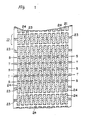
- Fig. 1 is a plane view of a Part of a metallized film embodying the invention.
- Fig. 2 is an enlarged plane view of a part of a metallized film
- Fig. 3 is a perspective view describing that the metallized film is subject to a strip tape-shape metallized film which is cut at right angles with the lengthwise direction of the film
- Fig, 4 is a perspective view of the tape shade metallized film described by Fig. 3 which comprises laminated films by altering the facing direction thereof at every film and a metallicon portion which is welded on both edge surfaces of the laminated film, and a partially section view of said metallicon is shown.
- Fig. 3 which comprises laminated films by altering the facing direction thereof at every film and a metallicon portion which is welded on both edge surfaces of the laminated film, and a partially section view of said metallicon is shown.
- FIG. 5 is a perspective view of the laminated film which is taken apart along the line U-U of Fig. 4
- Fig. 6 is a skeleton sectional view of one embodiment of a vacuum depositing apparatus which is used for producing a metallized film according to the present invention
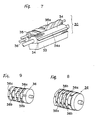
- Fig.7 is a perspective view of one embodiment of a masking oil transferring device which is disposed in the vacuum-depositing apparatus
- Figs. 8 and 9 are a partially enlarged perspective views of a pattern roll which forms the transferring device
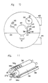
- Fig. 10 is a skeleton section view of the vacuum-depositing appratus used in the other embodiment of the invention.
- Fig. 11 is an enlarged perspective view of the masking oil transferring device disposed in the vacuum-depositing apparatus shown by Fig. 10.
- Figs. 12 to 14 are explanatory views of the conventional metallized film and the process of producing a laminated chip capacitor by using the same
- Fig, 12A is a plane view of the metallized film of itself
- Fig. 12B is a perspective view of the laminated metallized film on which the metallicon portion after laminating said film of itself is provided and an unit of the chip capacitor which is obtained by partially taking a part of said laminated film
- Fig. 12C is an enlarged section view taken along the line C-C of Fig. 12B
- Fig. 12D is an explanatory perspective view of the chip capacitor.
- Figs. 13A and 13B are plane views of a pattern of the metal deposited film which is deposited on the dielectric film surface
- Fig. 14A is also a plane view of the metallized film according to the other conventional method
- Fig. 14B is a perspective view of the laminating condition of the metallized film shown by Fig. 14B.
- FIG. 1 A typical depositing pattern of a metallized film for producing a laminated chip capacitor is shown in Fig. 1.
- the numeral 21 indicates a belt-like dielectric film and a metal deposited film which has a pattern indicated by a numeral 22 is formed on said film 21 to produce a metallized film.
- a metal deposited surface which has a skewered pattern or a backbone pattern is formed on the dielectric film surface.
- Said skewered pattern or backbone pattern 22 is composed whole of a continuous linear metal deposited film 23 which is disposed in a direction at right angles with the lengthwise direction of said film and a plurality of branch-shape metal deposited films 24, 24 extending bilaterally symmetrically from said deposited film 23 as to be a symmetrical axis.
- said skewered or backbone patterns 22 are formed in repeated patterns which have certain spaces toward the lengthwise direction of the dielectric film.
- a metallized film 21 as shown in Fig. 1 is taken apart from respective disconnecting lines S and T, the line S locates at the intermediary of each pattern and the line T passes the center line of the continuous linear-shape metal deposited film 23 which comprises a central axis of each pattern.
- Fig.2 is an explanatory view in which one unit of patterns is pick up from the continuous repeated pattern and the disconnecting line is added therein.
- the linear-shape metal deposited film 23 is disposed along one edge of the film 25a, 25b, a continuous horizontal margin portion 26 is formed on the other edge of the film along the lengthwise direction of the film and a vertical margin portion 27 is formed between carpenter's square-shape deposited films 24 which extend like a branch from the linear metal deposited film 23.
- Metallized films indicated by numerals 25a, 25b shown in Fig. 3 have all the same shape each other, a laminated film 28 is obtained only by alternately laminating each metallized film in which each facing direction is merely altered and is shown in Fig. 4.
- a metallicon portion 29 is formed by spraying a metal to both end surfaces of the laminated film 28 of Fig.
- a linear metal deposited film 28 exists through the whole area of the end surface of the laminated film to permit the area of the metal deposited film to be bigger in comparison with the conventional one and to permit the metallicon welded area on the metal deposited film to broaden, and resultantly a chip capacitor which has an excellent tan- ⁇ characteristic and an excellent withstand voltage characteristic which determines the quality thereof, is obtained.
- a method of producing a metallized film of the present invention will be described in detail in accordance with the embodiment.
- Fig. 6 is a side elevation view of a vacuum-depositing apparatus containing a device of transferring a masking oil to the dielectric film 21 in a predetermined pattern as described above.
- the metallized film used for the laminated chip capacitor is produced by using a transferring device indicated by a numeral 30. Including whole of the structure thereof, the vacuum-depositing apparatus will be described in detail hereinbelow.
- a reel 21' of a biaxial oriented polyether-ether-ketone film which has a thickness 12 ⁇ m is provided in a vacuum tank 31 (the vacuum degree is 10 ⁇ 2 Toor or below) and the dielectric film 21 is fed from an unreel 32 of said reel.
- the masking oil transferring device 30 which has a composition as described hereinafter is disposed through the way of the film 21 passing.
- the transferring device 30 is shown in detail by Figs. 7 to 9, the numeral 33 indicates a tank of the masking oil, the numeral 34 indicates a gravure roll partially dipping in the tank 33 and the masking oil is subject to be drawn up through intermediary of the gravure roll.
- the number of meshes on the gravure roll surface is preferably in a range of 200 to 600 mesh.
- the numeral 34a indicates a doctor
- 35 indicates an offset roll which contacts and rotates with the gravure roll 34 to transfer the oil drawn up by the gravure roll to the pattern roll which will be described hereinafter and a sponge roll of which roll surface is formed with a spiral groove 35a as shown in Figs. 7 to 9 is preferably used for the offset roll. In the present invention, it is not much necessary to use the offset roll.
- a roll indicated by the numeral 36 is the pattern roll and which surface is formed with the pattern comprising of rugged portions as described in Figs. 8 and 9, is used therefor.
- the roll surface is coated by a graving rubber sheet for producing a sealing print and said rubber sheet is previously graved the skewered or the backbone pattern so as to appear repeatedly
- Fig. 8 shows the convex face portion 36a of the roll surface which contains the skewered or the backbone pattern
- Fig. 9 shows the roll surface which is formed with the repeated pattern by the concave face portion 36b. It is possible to select any of patterns since said rugged portions are relative with each other.
- the predetermined skewered or backbone repeating pattern is formed on the roll peripheral surface by said rugged pattern and said repeating pattern is produced by a graving or other adequate method.
- the pattern roll 36 having a composition as described hereinbefore is disposed to contact and rotate with the offset roll 35, the pattern roll 36 is also attached to contact and rotate with a cooling can 40 in the vacuum-depositing appratus as shown in Fig. 6 and said roll 36 and the cooling can 40 are composed to receive the dielectric film 21 to be a material film which passes therebetween.
- silicone oil (Trade name, HIVAC F4 manufactured by Shin-etsu Chemical Ind.) is supplied to a tank 33 by the transferring device 30 which has a composition as described above, when the device 30 is operated, said masking oil is drawn up by the gravure roll 34, is leveled through a doctor 34a simultaneously and said masking oil is transferred to the pattern roll 36 surface after once transferred to the offset roll 35 which contacts and rotates with the roll 34. That is, in an embodiment described by Fig. 10, an oil drawn by said gravure roll, for example, is transferred to the offset roll comprising of a hard urethane resin foaming and then is transferred to the pattern roll which has a rubber made surface.
- the peripheral surface of the pattern roll 36 is composed of the rugged portions 36a and 36b, thereby only the convex face portion is subject to contact with the offset roll 35.
- the masking oil sticking on the offset roll 35 surface is transferred to only the surface of the convex face portion 36a of the pattern roll but not to stick on the concave face portion 36b. Since the pattern roll is subject to contact with the dielectric film 21 after sticking the oil on the convex face portion 36a of the pattern roll, a masking oil is transferred to the film surface in a form of providing a pattern which corresponds to the convex face portion of the pattern roll.
- a volume of the oil to stick on the pattern roll is adjustable by altering a mesh of the gravure roll so that the supplying volume of the oil is reduced by using a roll which has fine meshes (the number of meshes is many) and a sticking volume of the oil to the pattern roll is increased by a few of meshes, thereby the thick of the oil film formed on the dielectric film is adjusted.
- the doctor disposed on the roll of course works a supplemental role.
- the masking oil is provided on the dielectric film 21 surface in a condition of a pattern appearing as a voide portion shown in Fig. 1 ( a pattern except for a portion where is provided with a hatching). Further as described by Fig. 6, the dielectric film which has a condition of the oil film provided thereto in a pattern as described above is lead to a right under a zinc evaporating source. In the case as described above, the evaporating metal is deposited only the portion where the oil film does not exist but not the portion where the masking oil exits. The reason thereof is that the oil reevaporation occurrs on the metal evaporating source and a depositing function of the metal atom to the dielectric film is prevented by the oil molecular.
- a metal deposited film which has a repeated pattern of a skewered pattern or a backbone pattern is formed on the dielectric film surface and said processed film is wound by a winding reel 42 shown in Fig. 6 to be subject to an intermediate product for chip capacitors.
- the numeral 43 in Fig. 6 indicates a guide roll, 44 indicates a partition wall and 45 does an exhaust duct.
- a film is cut in a strip tape-shape along the disconnecting line indicated by numerals S and T in Figs. 1 and 2, are laminated as shown in Figs. 3 to 5, the metallicon portion 29 is formed thereon by spraying the metal and the laminated film is cut in square to obtain a laminated chip capacitor.
- the obtained laminated chip capacitors as described above have a withstand voltage of 1000 V and more and a good value of tan- ⁇ characteristic was obtained.
- the previous roughning process as described hereinafter is provided on the convex face portion 36a surface of said rubber sheet to be available of forming the oil film.
- the convex face portion is previously roughned by once or twice times of vertically and horizontally sides scratching by a sand paper ( # 500 of JIS standard is used therefor).
- the graving rubber sheet is coated on the pattern roll surface, the surface of the convex face portion of said rubber sheet is roughned in various directions by the sand paper regulated as described below, the oil film is formed by sticking a silicone oil ( Trade name, HIVAC F4 manufactured by Shin-etsu Chemical Ind.) on the pattern roll surface which has the roughned convex face portion as described above, and then obtained oil film is transferred to the polyester film surface.
- the oil transferred condition is inspected after transferring the oil by a process as described above several times.
- the the oil transferation degree is evaluated by obtaining the percentage(%) of the area where the irregular oil transferation on the film surface occurred. The result thereof will be shown in a following Table.
- the degree of the roughning is #500 and more.
- An appratus (a vacuum depositing appratus in vacuum 10 ⁇ 4 Torr) shown in Figs. 10 and 11 is used, aluminum is used as the depositing metal, perfuloro-alkyl-polyether oil (Trade name S-65 manufactured by Daikin Industries , a vapor pressure thereof is 1 x 10 ⁇ 4 Torr) is used as a masking oil and a metallized film having a pattern same as described in Example 1.
- the composition thereof is exactly same as described in Fig. 6 except of an alternation at the device 30 portion which transferrs the masking oil to the dielectric film.
- the different composition from the apparatus shown in Figs. 8 and 9 is only the masking oil transferring device and will be described hereinafter.
- the numeral 30 indicates the transferring device and which is enlarged in Fig. 11.
- the numeral 37 indicates an oil pot provided with a heater for carburetting or evaporating the masking oil.
- a slit-shape opening portion 37a is formed at the upper portion of the pot and an offset roll 38 is disposed abutting to the pot.
- the masking oil supplyed in the pot is carbureted or evaporated by an electric heater which is assembled in the pot.
- the vapor of said oil sticks on the offset roll 38 surface abutting to said opening.
- the oil is stuck on the offset roll 38 surface and said stuck oil is transferred to a pattern roll 36 which contacts and rotates with said offset roll.
- the surface of said pattern roll 36 as shown in Figs. 8 and 9, comprises the rugged portions 36a, 36b, as similar as described in Example 1, thereby the oil is transferred only to the convex face portion and does not stick on the concave face portion 36b.
- the metallized film of the present invention is composed of a repeated pattern in which a distributing condition of the metal deposited film to be formed on the dielectric film surface has an unit of a skewered or backbone pattern-shape, the linear deposited film forming the axis line of said pattern-shape and the branch-shape deposited film extending both directions of said linear deposited film are united independently to be metal deposited on the dielectric film surface. Resultantly, for obtaining a metallized film for a laminated chip capacitor, said metallized film is cut to a tape-shape at disconnecting lines which are a center line of said linear deposited film and a center line between each abutting branch-shape deposited films.
- the counter electrode is obtained by laminating each of films altering each facing direction.
- the metallized film for a chip capacitor of the present invention has an excellent effect that it is not necessary to produce metallized film having each different deposited condition for every counter electrodes and it is unnecessary to provide a special process therefor as the conventional method.
- the metallicon portion which is subject to an electrode output is completely deposited electrically through the whole width of the metallized film, thereby a capacitor is so obtained that the metallicon portion is prevented from sticking apparently on the margin portion of the dielectric film in different form a conventional method.
- the metallized film of the invention has an excellent effect of improving not only a withstand voltage characteristic of the chip capacitor of itself but also tan characteristic which determines the quality of this kind of capacitors.
- a method of the present invention in producing the metallized film having the composition as described hereinbefore, since a very practicable method for industrial is developed that it is sufficient only by depositing a metal after transferring a masking oil to the dielectric film surface by a printing system through an intermediary of the transferring device which is substantially composed of the pattern roll having a special pattern-shape, a method of the present invention has a benefit of easy utility.
- the industrial applicability of the present invention is so high that a metallized film sufficiently satisfys the demand of laminated chip capacitors recently increasing in accordance with the progress of the electronics and improves the quality of chip capacitors obtained thereby.
Landscapes
- Engineering & Computer Science (AREA)
- Power Engineering (AREA)
- Chemical & Material Sciences (AREA)
- Manufacturing & Machinery (AREA)
- Microelectronics & Electronic Packaging (AREA)
- Chemical Kinetics & Catalysis (AREA)
- Materials Engineering (AREA)
- Mechanical Engineering (AREA)
- Metallurgy (AREA)
- Organic Chemistry (AREA)
- Fixed Capacitors And Capacitor Manufacturing Machines (AREA)
- Physical Vapour Deposition (AREA)
Abstract
Applications Claiming Priority (3)
| Application Number | Priority Date | Filing Date | Title |
|---|---|---|---|
| JP30779988 | 1988-12-07 | ||
| JP307799/88 | 1988-12-07 | ||
| PCT/JP1989/001229 WO1990006586A1 (fr) | 1988-12-07 | 1989-12-07 | Film metallise pour condensateurs de circuits intergres feuilletes et procede de production |
Publications (3)
| Publication Number | Publication Date |
|---|---|
| EP0447550A1 true EP0447550A1 (fr) | 1991-09-25 |
| EP0447550A4 EP0447550A4 (en) | 1992-12-02 |
| EP0447550B1 EP0447550B1 (fr) | 1997-04-09 |
Family
ID=17973369
Family Applications (1)
| Application Number | Title | Priority Date | Filing Date |
|---|---|---|---|
| EP90900328A Expired - Lifetime EP0447550B1 (fr) | 1988-12-07 | 1989-12-07 | Procede de production d'un film metallise pour condensateurs de circuits intergres feuilletes |
Country Status (5)
| Country | Link |
|---|---|
| EP (1) | EP0447550B1 (fr) |
| JP (1) | JPH02263419A (fr) |
| KR (2) | KR910700536A (fr) |
| DE (1) | DE68927959T2 (fr) |
| WO (1) | WO1990006586A1 (fr) |
Cited By (11)
| Publication number | Priority date | Publication date | Assignee | Title |
|---|---|---|---|---|
| US5223038A (en) * | 1991-01-11 | 1993-06-29 | Leybold Ag | Apparatus for producing metal-free strips |
| EP1693481A1 (fr) | 2005-11-23 | 2006-08-23 | Galileo Vacuum Systems S.R.L. | Chambre de métallisation sous vide avec systèmes pour dépot partiel |
| CN1298550C (zh) * | 2003-04-17 | 2007-02-07 | 株式会社村田制作所 | 凹版印刷机及多层陶瓷电子元件的制造方法 |
| EP1978126A1 (fr) * | 2007-04-03 | 2008-10-08 | Applied Materials, Inc. | Appareil de revêtement en continu d'un substrat en forme de bande |
| EP1990442A1 (fr) | 2007-03-27 | 2008-11-12 | Galileo Vacuum Systems S.p.A. | Dispositif de dépôt sous vide d'un revêtement sur un matériau continu, avec applicateur liquide |
| CN1974207B (zh) * | 2003-04-17 | 2010-11-17 | 株式会社村田制作所 | 凹版印刷滚筒 |
| EP2071051A4 (fr) * | 2006-10-06 | 2012-01-04 | Ulvac Inc | Appareil de filmage sous vide du type avec tendeur |
| US8169014B2 (en) | 2006-01-09 | 2012-05-01 | Taiwan Semiconductor Manufacturing Co., Ltd. | Interdigitated capacitive structure for an integrated circuit |
| JP2015170779A (ja) * | 2014-03-07 | 2015-09-28 | 株式会社村田製作所 | 積層型フィルムコンデンサ、コンデンサモジュール、および電力変換システム |
| US11817272B2 (en) | 2017-08-15 | 2023-11-14 | Oji Holdings Corporation | Metallized film, metallized film roll, plate roll |
| WO2025085798A1 (fr) * | 2023-10-20 | 2025-04-24 | Applied Materials, Inc. | Tambour d'échange de chaleur revêtu de céramique doté de buses, de mesas de non-étanchéité et de mesas d'étanchéité |
Families Citing this family (7)
| Publication number | Priority date | Publication date | Assignee | Title |
|---|---|---|---|---|
| DE19734477B4 (de) * | 1996-08-09 | 2005-11-03 | Matsushita Electric Industrial Co., Ltd., Kadoma | Metallisierter Filmkondensator und Vorrichtung und Verfahren für die Herstellung eines metallisierten Films für den metallisierten Filmkondensator |
| KR100483944B1 (ko) * | 2000-04-14 | 2005-04-15 | 마쯔시다덴기산교 가부시키가이샤 | 적층체, 콘덴서, 전자부품 및 이들의 제조 방법과 제조 장치 |
| JP2008124245A (ja) * | 2006-11-13 | 2008-05-29 | Matsushita Electric Ind Co Ltd | 金属化フィルムの製造装置と金属化フィルムの製造方法 |
| JP5450348B2 (ja) * | 2010-10-27 | 2014-03-26 | 小島プレス工業株式会社 | 金属化フィルムの製造装置 |
| KR101422938B1 (ko) * | 2012-12-04 | 2014-07-23 | 삼성전기주식회사 | 기판 내장용 적층 세라믹 전자부품 및 이의 제조방법, 기판 내장용 적층 세라믹 전자부품을 구비하는 인쇄회로기판 |
| JP6383933B1 (ja) * | 2018-02-02 | 2018-09-05 | 王子ホールディングス株式会社 | 金属化フィルム、版ロール |
| CN116479373A (zh) * | 2022-01-13 | 2023-07-25 | 宁德时代新能源科技股份有限公司 | 镀膜设备 |
Family Cites Families (8)
| Publication number | Priority date | Publication date | Assignee | Title |
|---|---|---|---|---|
| NL69653C (fr) * | 1945-08-14 | 1952-02-16 | ||
| LU42919A1 (fr) * | 1962-12-21 | 1963-02-21 | ||
| GB1106364A (en) * | 1964-03-04 | 1968-03-13 | Bostik Ltd | Improvements in or relating to metallized surfaces |
| JPS5158649A (en) * | 1974-11-15 | 1976-05-22 | Matsushita Electric Industrial Co Ltd | Ratsukaamaajinno keiseihoho |
| JPS57177518A (en) * | 1981-04-24 | 1982-11-01 | Tdk Electronics Co Ltd | Laminated condenser and method of producing same |
| IT1185177B (it) * | 1985-07-03 | 1987-11-04 | Metalvuoto Films Spa | Dispositivo per realizzare film plastici metallizzati presentanti zone ben delimitate prive di metallizzazione |
| JPS6240714A (ja) * | 1985-08-16 | 1987-02-21 | 株式会社村田製作所 | 積層コンデンサの製造方法 |
| DE3725454A1 (de) * | 1987-07-31 | 1989-02-09 | Siemens Ag | Elektrisches vielschichtbauelement mit einem gesinterten, monolithischen keramikkoerper und verfahren zur herstellung des elektrischen vielschichtbauelementes |
-
1989
- 1989-12-07 EP EP90900328A patent/EP0447550B1/fr not_active Expired - Lifetime
- 1989-12-07 KR KR1019900701719A patent/KR910700536A/ko active Granted
- 1989-12-07 JP JP1316472A patent/JPH02263419A/ja active Pending
- 1989-12-07 KR KR1019900701719A patent/KR930010422B1/ko not_active Expired - Fee Related
- 1989-12-07 WO PCT/JP1989/001229 patent/WO1990006586A1/fr not_active Ceased
- 1989-12-07 DE DE68927959T patent/DE68927959T2/de not_active Expired - Fee Related
Cited By (13)
| Publication number | Priority date | Publication date | Assignee | Title |
|---|---|---|---|---|
| US5223038A (en) * | 1991-01-11 | 1993-06-29 | Leybold Ag | Apparatus for producing metal-free strips |
| EP0494340B1 (fr) * | 1991-01-11 | 1995-03-15 | Leybold Aktiengesellschaft | Dispositif pour l'obtention de raies exemptes de métal |
| CN1974207B (zh) * | 2003-04-17 | 2010-11-17 | 株式会社村田制作所 | 凹版印刷滚筒 |
| CN1298550C (zh) * | 2003-04-17 | 2007-02-07 | 株式会社村田制作所 | 凹版印刷机及多层陶瓷电子元件的制造方法 |
| EP1693481A1 (fr) | 2005-11-23 | 2006-08-23 | Galileo Vacuum Systems S.R.L. | Chambre de métallisation sous vide avec systèmes pour dépot partiel |
| US8169014B2 (en) | 2006-01-09 | 2012-05-01 | Taiwan Semiconductor Manufacturing Co., Ltd. | Interdigitated capacitive structure for an integrated circuit |
| EP2071051A4 (fr) * | 2006-10-06 | 2012-01-04 | Ulvac Inc | Appareil de filmage sous vide du type avec tendeur |
| EP1990442A1 (fr) | 2007-03-27 | 2008-11-12 | Galileo Vacuum Systems S.p.A. | Dispositif de dépôt sous vide d'un revêtement sur un matériau continu, avec applicateur liquide |
| EP1978126A1 (fr) * | 2007-04-03 | 2008-10-08 | Applied Materials, Inc. | Appareil de revêtement en continu d'un substrat en forme de bande |
| US7984689B2 (en) | 2007-04-03 | 2011-07-26 | Applied Materials, Inc. | Device for the continuous coating of a strip-like substrate |
| JP2015170779A (ja) * | 2014-03-07 | 2015-09-28 | 株式会社村田製作所 | 積層型フィルムコンデンサ、コンデンサモジュール、および電力変換システム |
| US11817272B2 (en) | 2017-08-15 | 2023-11-14 | Oji Holdings Corporation | Metallized film, metallized film roll, plate roll |
| WO2025085798A1 (fr) * | 2023-10-20 | 2025-04-24 | Applied Materials, Inc. | Tambour d'échange de chaleur revêtu de céramique doté de buses, de mesas de non-étanchéité et de mesas d'étanchéité |
Also Published As
| Publication number | Publication date |
|---|---|
| KR910700536A (ko) | 1991-03-15 |
| EP0447550B1 (fr) | 1997-04-09 |
| KR930010422B1 (ko) | 1993-10-23 |
| JPH02263419A (ja) | 1990-10-26 |
| DE68927959T2 (de) | 1997-11-27 |
| WO1990006586A1 (fr) | 1990-06-14 |
| DE68927959D1 (de) | 1997-05-15 |
| EP0447550A4 (en) | 1992-12-02 |
Similar Documents
| Publication | Publication Date | Title |
|---|---|---|
| EP0447550B1 (fr) | Procede de production d'un film metallise pour condensateurs de circuits intergres feuilletes | |
| US5774326A (en) | Multilayer capacitors using amorphous hydrogenated carbon | |
| KR880008356A (ko) | 전해콘덴서용 알루미늄 전극재료 및 그 재조방법 | |
| EP0158971B1 (fr) | Contacts latéraux pour condensateur monolithique | |
| EP1005260A3 (fr) | Formation de condensateurs à couche mince | |
| EP0509560A3 (fr) | Condensateur électrolytique solide du type enroulé | |
| SE8400418L (sv) | Elektrod med lang livslengd for elektrolysendamal och forfarande for framstellning av densamma | |
| US5179773A (en) | Process of manufacturing multilayer ceramic capacitors | |
| JP3720846B2 (ja) | 複数の電子多層構成部品の製造方法 | |
| EP0242461B1 (fr) | Condensateur électrique monolithique miniature | |
| US2709663A (en) | Electrical capacitors | |
| US3365378A (en) | Method of fabricating film-forming metal capacitors | |
| EP0843327B1 (fr) | Condensateur à film métallisé | |
| SE454630B (sv) | Lindad kondensator samt sett och anordning for framstellning av densamma | |
| US4667382A (en) | Method for manufacturing electrical capacitors | |
| CA1140642A (fr) | Condensateur d'electrolyse a cathode de grande purete | |
| JPS6025217A (ja) | コンデンサ形成用金属化フイルム及び該フイルムからのコンデンサ製造方法 | |
| US3668482A (en) | An offset, wound, single-web roll capacitor and process for making same | |
| JPS637363A (ja) | 真空蒸着方法 | |
| US2802256A (en) | Electric condensers | |
| JPS59103323A (ja) | コンデンサ用金属蒸着フイルムの製造方法 | |
| KR820000815B1 (ko) | 다층막(多層膜) 증착법(蒸眼法) | |
| JPH0436569B2 (fr) | ||
| JP3447307B2 (ja) | フィルムコンデンサおよびその製造用フィルム | |
| KR0130868B1 (ko) | 다층 칩 캐패시터(Multilayer Chip Capacitor)의 외부 전극 제조방법 |
Legal Events
| Date | Code | Title | Description |
|---|---|---|---|
| PUAI | Public reference made under article 153(3) epc to a published international application that has entered the european phase |
Free format text: ORIGINAL CODE: 0009012 |
|
| 17P | Request for examination filed |
Effective date: 19910606 |
|
| AK | Designated contracting states |
Kind code of ref document: A1 Designated state(s): DE FR GB IT |
|
| A4 | Supplementary search report drawn up and despatched |
Effective date: 19921012 |
|
| AK | Designated contracting states |
Kind code of ref document: A4 Designated state(s): DE FR GB IT |
|
| 17Q | First examination report despatched |
Effective date: 19930504 |
|
| GRAG | Despatch of communication of intention to grant |
Free format text: ORIGINAL CODE: EPIDOS AGRA |
|
| GRAH | Despatch of communication of intention to grant a patent |
Free format text: ORIGINAL CODE: EPIDOS IGRA |
|
| GRAH | Despatch of communication of intention to grant a patent |
Free format text: ORIGINAL CODE: EPIDOS IGRA |
|
| GRAA | (expected) grant |
Free format text: ORIGINAL CODE: 0009210 |
|
| AK | Designated contracting states |
Kind code of ref document: B1 Designated state(s): DE FR GB IT |
|
| RAP2 | Party data changed (patent owner data changed or rights of a patent transferred) |
Owner name: OJI PAPER CO., LTD. |
|
| REF | Corresponds to: |
Ref document number: 68927959 Country of ref document: DE Date of ref document: 19970515 |
|
| ET | Fr: translation filed | ||
| PLBE | No opposition filed within time limit |
Free format text: ORIGINAL CODE: 0009261 |
|
| STAA | Information on the status of an ep patent application or granted ep patent |
Free format text: STATUS: NO OPPOSITION FILED WITHIN TIME LIMIT |
|
| 26N | No opposition filed | ||
| REG | Reference to a national code |
Ref country code: GB Ref legal event code: IF02 |
|
| REG | Reference to a national code |
Ref country code: FR Ref legal event code: ST |
|
| REG | Reference to a national code |
Ref country code: FR Ref legal event code: RN |
|
| REG | Reference to a national code |
Ref country code: FR Ref legal event code: FC |
|
| PGFP | Annual fee paid to national office [announced via postgrant information from national office to epo] |
Ref country code: DE Payment date: 20061130 Year of fee payment: 18 |
|
| PGFP | Annual fee paid to national office [announced via postgrant information from national office to epo] |
Ref country code: GB Payment date: 20061206 Year of fee payment: 18 |
|
| PGFP | Annual fee paid to national office [announced via postgrant information from national office to epo] |
Ref country code: FR Payment date: 20061208 Year of fee payment: 18 |
|
| PGFP | Annual fee paid to national office [announced via postgrant information from national office to epo] |
Ref country code: IT Payment date: 20061231 Year of fee payment: 18 |
|
| GBPC | Gb: european patent ceased through non-payment of renewal fee |
Effective date: 20071207 |
|
| PG25 | Lapsed in a contracting state [announced via postgrant information from national office to epo] |
Ref country code: DE Free format text: LAPSE BECAUSE OF NON-PAYMENT OF DUE FEES Effective date: 20080701 |
|
| REG | Reference to a national code |
Ref country code: FR Ref legal event code: ST Effective date: 20081020 |
|
| PG25 | Lapsed in a contracting state [announced via postgrant information from national office to epo] |
Ref country code: GB Free format text: LAPSE BECAUSE OF NON-PAYMENT OF DUE FEES Effective date: 20071207 |
|
| PG25 | Lapsed in a contracting state [announced via postgrant information from national office to epo] |
Ref country code: FR Free format text: LAPSE BECAUSE OF NON-PAYMENT OF DUE FEES Effective date: 20071231 |
|
| PG25 | Lapsed in a contracting state [announced via postgrant information from national office to epo] |
Ref country code: IT Free format text: LAPSE BECAUSE OF NON-PAYMENT OF DUE FEES Effective date: 20071207 |