EP0447767B1 - Verfahren zum Herstellen orientierter polykristalliner supraleitender keramischer Oxide - Google Patents
Verfahren zum Herstellen orientierter polykristalliner supraleitender keramischer Oxide Download PDFInfo
- Publication number
- EP0447767B1 EP0447767B1 EP91101250A EP91101250A EP0447767B1 EP 0447767 B1 EP0447767 B1 EP 0447767B1 EP 91101250 A EP91101250 A EP 91101250A EP 91101250 A EP91101250 A EP 91101250A EP 0447767 B1 EP0447767 B1 EP 0447767B1
- Authority
- EP
- European Patent Office
- Prior art keywords
- ceramic oxide
- composite structure
- process according
- superconducting
- substrate
- Prior art date
- Legal status (The legal status is an assumption and is not a legal conclusion. Google has not performed a legal analysis and makes no representation as to the accuracy of the status listed.)
- Expired - Lifetime
Links
- 239000000919 ceramic Substances 0.000 title claims description 83
- 238000000034 method Methods 0.000 title claims description 55
- 239000000463 material Substances 0.000 claims description 50
- 239000000758 substrate Substances 0.000 claims description 50
- 230000008569 process Effects 0.000 claims description 41
- 239000002131 composite material Substances 0.000 claims description 40
- 229910021521 yttrium barium copper oxide Inorganic materials 0.000 claims description 25
- 238000000137 annealing Methods 0.000 claims description 20
- 238000001816 cooling Methods 0.000 claims description 17
- 238000010438 heat treatment Methods 0.000 claims description 13
- 238000000151 deposition Methods 0.000 claims description 11
- 239000000203 mixture Substances 0.000 claims description 11
- QVGXLLKOCUKJST-UHFFFAOYSA-N atomic oxygen Chemical compound [O] QVGXLLKOCUKJST-UHFFFAOYSA-N 0.000 claims description 9
- 239000001301 oxygen Substances 0.000 claims description 9
- 229910052760 oxygen Inorganic materials 0.000 claims description 9
- 230000008018 melting Effects 0.000 claims description 7
- 238000002844 melting Methods 0.000 claims description 7
- 229910003098 YBa2Cu3O7−x Inorganic materials 0.000 claims description 6
- 230000008021 deposition Effects 0.000 claims description 5
- 150000001875 compounds Chemical class 0.000 claims description 4
- 238000010587 phase diagram Methods 0.000 claims description 4
- 239000002904 solvent Substances 0.000 claims description 4
- 238000004544 sputter deposition Methods 0.000 claims description 4
- 238000001704 evaporation Methods 0.000 claims description 3
- 238000010884 ion-beam technique Methods 0.000 claims description 3
- 238000004519 manufacturing process Methods 0.000 claims description 3
- 238000005137 deposition process Methods 0.000 claims description 2
- 230000009977 dual effect Effects 0.000 claims description 2
- 238000005530 etching Methods 0.000 claims description 2
- 238000007750 plasma spraying Methods 0.000 claims description 2
- 239000002887 superconductor Substances 0.000 description 61
- 239000010408 film Substances 0.000 description 33
- 239000013078 crystal Substances 0.000 description 17
- 239000012071 phase Substances 0.000 description 15
- 238000000576 coating method Methods 0.000 description 12
- 238000012545 processing Methods 0.000 description 11
- 238000002441 X-ray diffraction Methods 0.000 description 9
- 239000011248 coating agent Substances 0.000 description 9
- 239000010409 thin film Substances 0.000 description 6
- 230000015572 biosynthetic process Effects 0.000 description 4
- 239000012535 impurity Substances 0.000 description 4
- 230000004888 barrier function Effects 0.000 description 3
- 239000007788 liquid Substances 0.000 description 3
- 239000000843 powder Substances 0.000 description 3
- 238000009718 spray deposition Methods 0.000 description 3
- 238000004857 zone melting Methods 0.000 description 3
- XKRFYHLGVUSROY-UHFFFAOYSA-N Argon Chemical compound [Ar] XKRFYHLGVUSROY-UHFFFAOYSA-N 0.000 description 2
- IJGRMHOSHXDMSA-UHFFFAOYSA-N Atomic nitrogen Chemical compound N#N IJGRMHOSHXDMSA-UHFFFAOYSA-N 0.000 description 2
- XUIMIQQOPSSXEZ-UHFFFAOYSA-N Silicon Chemical compound [Si] XUIMIQQOPSSXEZ-UHFFFAOYSA-N 0.000 description 2
- 239000000654 additive Substances 0.000 description 2
- 230000008901 benefit Effects 0.000 description 2
- 238000012512 characterization method Methods 0.000 description 2
- 238000011109 contamination Methods 0.000 description 2
- RKTYLMNFRDHKIL-UHFFFAOYSA-N copper;5,10,15,20-tetraphenylporphyrin-22,24-diide Chemical compound [Cu+2].C1=CC(C(=C2C=CC([N-]2)=C(C=2C=CC=CC=2)C=2C=CC(N=2)=C(C=2C=CC=CC=2)C2=CC=C3[N-]2)C=2C=CC=CC=2)=NC1=C3C1=CC=CC=C1 RKTYLMNFRDHKIL-UHFFFAOYSA-N 0.000 description 2
- 230000002950 deficient Effects 0.000 description 2
- 230000000694 effects Effects 0.000 description 2
- 230000008020 evaporation Effects 0.000 description 2
- 230000003993 interaction Effects 0.000 description 2
- 230000007246 mechanism Effects 0.000 description 2
- 239000000155 melt Substances 0.000 description 2
- 238000006213 oxygenation reaction Methods 0.000 description 2
- 229910052710 silicon Inorganic materials 0.000 description 2
- 239000010703 silicon Substances 0.000 description 2
- 229910000108 silver(I,III) oxide Inorganic materials 0.000 description 2
- 239000000126 substance Substances 0.000 description 2
- MYMOFIZGZYHOMD-UHFFFAOYSA-N Dioxygen Chemical compound O=O MYMOFIZGZYHOMD-UHFFFAOYSA-N 0.000 description 1
- 229910002370 SrTiO3 Inorganic materials 0.000 description 1
- 230000000996 additive effect Effects 0.000 description 1
- 230000002411 adverse Effects 0.000 description 1
- PNEYBMLMFCGWSK-UHFFFAOYSA-N aluminium oxide Inorganic materials [O-2].[O-2].[O-2].[Al+3].[Al+3] PNEYBMLMFCGWSK-UHFFFAOYSA-N 0.000 description 1
- 229910052786 argon Inorganic materials 0.000 description 1
- 125000004429 atom Chemical group 0.000 description 1
- 230000009286 beneficial effect Effects 0.000 description 1
- 150000004649 carbonic acid derivatives Chemical class 0.000 description 1
- 230000015556 catabolic process Effects 0.000 description 1
- 230000008859 change Effects 0.000 description 1
- 230000001427 coherent effect Effects 0.000 description 1
- 230000008602 contraction Effects 0.000 description 1
- 238000007796 conventional method Methods 0.000 description 1
- 238000002425 crystallisation Methods 0.000 description 1
- 230000008025 crystallization Effects 0.000 description 1
- 238000000354 decomposition reaction Methods 0.000 description 1
- 230000007547 defect Effects 0.000 description 1
- 238000006731 degradation reaction Methods 0.000 description 1
- 238000000280 densification Methods 0.000 description 1
- 238000010586 diagram Methods 0.000 description 1
- 238000009792 diffusion process Methods 0.000 description 1
- 229910001882 dioxygen Inorganic materials 0.000 description 1
- 238000010894 electron beam technology Methods 0.000 description 1
- 230000005496 eutectics Effects 0.000 description 1
- 239000007789 gas Substances 0.000 description 1
- 239000001307 helium Substances 0.000 description 1
- 229910052734 helium Inorganic materials 0.000 description 1
- SWQJXJOGLNCZEY-UHFFFAOYSA-N helium atom Chemical compound [He] SWQJXJOGLNCZEY-UHFFFAOYSA-N 0.000 description 1
- 230000004941 influx Effects 0.000 description 1
- 239000012212 insulator Substances 0.000 description 1
- 238000010406 interfacial reaction Methods 0.000 description 1
- 239000007791 liquid phase Substances 0.000 description 1
- 238000005259 measurement Methods 0.000 description 1
- 229910052751 metal Inorganic materials 0.000 description 1
- 239000002184 metal Substances 0.000 description 1
- 150000002739 metals Chemical class 0.000 description 1
- 229910052757 nitrogen Inorganic materials 0.000 description 1
- 230000003647 oxidation Effects 0.000 description 1
- 238000007254 oxidation reaction Methods 0.000 description 1
- 125000004430 oxygen atom Chemical group O* 0.000 description 1
- 238000004806 packaging method and process Methods 0.000 description 1
- 239000002245 particle Substances 0.000 description 1
- 230000037361 pathway Effects 0.000 description 1
- 238000000059 patterning Methods 0.000 description 1
- 230000002265 prevention Effects 0.000 description 1
- 230000005855 radiation Effects 0.000 description 1
- 238000001953 recrystallisation Methods 0.000 description 1
- 229910052594 sapphire Inorganic materials 0.000 description 1
- 239000010980 sapphire Substances 0.000 description 1
- 238000005245 sintering Methods 0.000 description 1
- 238000010583 slow cooling Methods 0.000 description 1
- 239000007790 solid phase Substances 0.000 description 1
- 238000007711 solidification Methods 0.000 description 1
- 230000008023 solidification Effects 0.000 description 1
- 238000000992 sputter etching Methods 0.000 description 1
- 238000010561 standard procedure Methods 0.000 description 1
- 230000000699 topical effect Effects 0.000 description 1
- 230000007704 transition Effects 0.000 description 1
- 238000011282 treatment Methods 0.000 description 1
- 239000013598 vector Substances 0.000 description 1
Images


Classifications
-
- H—ELECTRICITY
- H10—SEMICONDUCTOR DEVICES; ELECTRIC SOLID-STATE DEVICES NOT OTHERWISE PROVIDED FOR
- H10N—ELECTRIC SOLID-STATE DEVICES NOT OTHERWISE PROVIDED FOR
- H10N60/00—Superconducting devices
- H10N60/01—Manufacture or treatment
- H10N60/0268—Manufacture or treatment of devices comprising copper oxide
- H10N60/0296—Processes for depositing or forming copper oxide superconductor layers
- H10N60/0548—Processes for depositing or forming copper oxide superconductor layers by deposition and subsequent treatment, e.g. oxidation of pre-deposited material
-
- Y—GENERAL TAGGING OF NEW TECHNOLOGICAL DEVELOPMENTS; GENERAL TAGGING OF CROSS-SECTIONAL TECHNOLOGIES SPANNING OVER SEVERAL SECTIONS OF THE IPC; TECHNICAL SUBJECTS COVERED BY FORMER USPC CROSS-REFERENCE ART COLLECTIONS [XRACs] AND DIGESTS
- Y10—TECHNICAL SUBJECTS COVERED BY FORMER USPC
- Y10S—TECHNICAL SUBJECTS COVERED BY FORMER USPC CROSS-REFERENCE ART COLLECTIONS [XRACs] AND DIGESTS
- Y10S505/00—Superconductor technology: apparatus, material, process
- Y10S505/725—Process of making or treating high tc, above 30 k, superconducting shaped material, article, or device
- Y10S505/733—Rapid solidification, e.g. quenching, gas-atomizing, melt-spinning, roller-quenching
-
- Y—GENERAL TAGGING OF NEW TECHNOLOGICAL DEVELOPMENTS; GENERAL TAGGING OF CROSS-SECTIONAL TECHNOLOGIES SPANNING OVER SEVERAL SECTIONS OF THE IPC; TECHNICAL SUBJECTS COVERED BY FORMER USPC CROSS-REFERENCE ART COLLECTIONS [XRACs] AND DIGESTS
- Y10—TECHNICAL SUBJECTS COVERED BY FORMER USPC
- Y10S—TECHNICAL SUBJECTS COVERED BY FORMER USPC CROSS-REFERENCE ART COLLECTIONS [XRACs] AND DIGESTS
- Y10S505/00—Superconductor technology: apparatus, material, process
- Y10S505/725—Process of making or treating high tc, above 30 k, superconducting shaped material, article, or device
- Y10S505/742—Annealing
Definitions
- the present invention relates generally to oriented, polycrystalline, high-temperature superconducting ceramic oxides and, more particularly, to a process for preparing such superconductors from bilayer structures.
- Superconductors are materials that, at sufficiently low temperatures and for sufficiently weak magnetic fields, have zero electrical resistivity. Absent electrical resistivity and the heat such resistivity creates, it would theoretically be possible for a superconductor to carry very large currents. As the current carried by a superconductor increases, however, a stronger and stronger magnetic field is self-generated until the critical magnetic field, above which the superconductor reverts to a normal conducting state with commensurate resistivity, is exceeded. Thus, there is a limit, the critical current density, to the amount of current a superconductor can carry.
- High-temperature superconductors (those which superconduct above 77 Kelvin) are structurally related to the crystallographic family known as perovskites, ceramics that have a distinct atomic arrangement and that are found as common natural materials. Both natural and synthetic perovskites exhibit a wide range of electrical properties. One such property in the perovskites which are superconducting, the critical current density, is of great importance in the practical application of high-temperature superconductors.
- the new, high-temperature superconductors have potential use at temperatures much higher than the extemely low temperatures required for superconduction by their older counterparts, they are inferior in other ways. Specifically, unlike older superconductors, the new, high-temperature superconductors lose their superconductivity under relatively small loads when polycrystalline and, consequently, are unable to carry sufficient current for practical applications.
- researchers are now attempting to develop high-temperature superconductors having sufficiently high critical current densities for use in practical applications; no matter how high the critical temperature of a superconductor, it is practically useless unless able to support a useful flow of electric current.
- a new, promising, high-temperature superconducting material is, for instance, the ceramic oxide YBa2Cu3O 7-x (0 ⁇ x ⁇ 0.5).
- This material is designated the "123 superconductor” because the atomic ratios of Y:Ba:Cu are approximately 1:2:3.
- the 123 superconductor normally is a highly twinned orthorhombic phase, which is believed responsible for superconduction, and is closely related to a tetragonal, nonsuperconducting phase (YBa2Cu3O6).
- the only significant difference between the nonsuperconducting, oxygen-deficient phase and the superconducting phase is the presence in the superconducting phase of Cu-O-Cu chains along the b-axis direction on the a-c faces of the unit cell.
- the 123 superconductor like many of the new, high-temperature superconductors, is anisotropic, meaning that crystals of the material conduct current better in one direction than in other directions. Some high-temperature superconductors can carry current thirty times more readily in one direction than in another direction. Because superconductivity is inhomogeneous on an atomic scale and localized to specific layers, current in the 123 superconductor flows poorly in one direction (the vertical direction, or c-axis of the unit cell, where c is the longest unit cell dimension) and easily in two directions (the a-b plane). In a polycrystalline material, the structure consists of an assembly of small, individual crystallites, whose relative orientation to each other may vary. Thus, orientation of the individual crystals in a bulk sample (as opposed to a single crystal) of the polycrystalline material is critical in determining the electrical properties.
- phase boundaries, grain boundaries, defects, and impurities may limit the current-carrying capacity.
- grains tend to line up randomly in bulk materials and current has a difficult time flowing through randomly oriented grains. J. Mannhart, P. Chaudhari, D. Dimos, C.C. Tsuei & T.R. Mc Guire, Critical Currents in [001] Grains and Across Their Tilt Boundaries in YBa2Cu3O7 Films , Phys. Rev. Lett. 61 2476 (1988).
- Impurities such as the carbonates which form easily in Ba-containing compounds lying between grains in bulk samples also make it harder for current to pass from grain to grain, which lowers the critical current density. Again, the growth orientation of the crystals in a polycrystalline material is important.
- a superconductor such as the 123 superconductor develops a path or track through its internal structure along which electrons are free to pass.
- the preferred orientation or texture has been shown for very thin films, those less than 1 micrometer thick, to have the c-axis perpendicular to the film surface.
- Such an orientation produces high critical current.
- the metallurgical formation of the material directly affects critical current density.
- the crystals form a random polycrystalline array.
- high critical current density can be obtained in the 123 superconductor only when there is a continuous current path along the base plane of the unit cell.
- a necessary condition to attain a high critical current density in polycrystalline superconducting ceramic oxides such as the 123 superconductor is to achieve the proper orientation in such materials.
- the 123 superconductor must have an orientation in which the c-axis of the unit cell is oriented normal to the substrate material (and to the plane of the superconductor film). This condition is necessary but not sufficient to achieve high critical current density.
- a number of processes have been developed to produce oriented superconducting ceramic oxides like the 123 superconductor.
- One method consists of introducing an additive, Ag2O, in powder form to the 123 superconductor ceramic oxide powder during processing.
- Ag2O an additive
- a modest increase in the critical current density by a factor of up to five is obtained. The increase is attributed to an increase in the orientation or texture (grain alignment) of the polycrystalline samples.
- M.K. Malik, V.D. Nair, A.R. Biswas & R.V. Raghavan Texture Formation and Enhanced Critical Current in YBa2Cu3O7 , Appl. Phys. Lett. 52 (18), 1525-27 (May 2, 1988).
- oriented thin films of 123 superconductors with crystallites having the c-axis of the unit cell normal to the plane of the superconductor film, have been produced by sputtering and evaporation onto substrates such as SrTiO3 and MgO.
- substrates such as SrTiO3 and MgO.
- the substrate or base layer must be carefully matched with the superconductor in existing thin film applications.
- the substrate's crystalline structure should be identical to that of the superconductor so that the thin film can be deposited with a minimum of flaws and dislocations.
- the superconductivity may degrade. Degradation may result because superconductors are very sensitive to an influx of foreign atoms. For example, interdiffusion can completely destroy superconductivity if the substrate contains even just a few percent silicon.
- melt-textured growth, or directional spherulitic growth, processing represents still another method available to achieve orientation.
- Conventional processing of ceramic oxide superconductors includes a sintering step in which the superconductor is fired at relatively low temperatures (about 700°C for the 123 superconductor) to sinter individual grains together.
- the sintered material exhibits a somewhat porous, fine-grained, and randomly oriented microstructure.
- melt-textured growth in contrast, the superconductor is melted at very high temperatures (about 1050-1200°C for the 123 superconductor) and slowly cooled to obtain directional solidification.
- the resulting material consists of long, needle-like crystals and grains that are preferentially aligned in roughly the same direction.
- the material is also more dense and shows enhanced decomposition of unwanted impurities relative to the sintered material.
- melt-textured growth process produces large grain growth and induces significant (near 100%) densification. Such properties tend to cause microcracking during the processing step of cooling, because the material cannot absorb the stress of the change in crystalline structure as YBa2Cu3O6 converts into YBa2Cu3O7. Problems also arise in the final processing step: oxygenation is made more difficult by the dense microstructure. Both of these undesirable features limit the critical current density possible and adversely affect other properties as well.
- the polycrystalline material, shown deposited on substrate 10 has relatively fine grains 12 .
- gates 14 are formed.
- a narrow annealing (or "hot") zone 16 then is moved along the film surface (from left to right in the figures) and the annealing temperature is adjusted so the grains of the polyscrystalline film grow (while in the annealing zone) into larger grains 18 ; the etched gates are formed so that the width of the gate opening or pinch-off zone 20 is slightly smaller than the grain size obtained during annealing.
- the region with the larger growing grains is moved along the film surface along with the annealing zone.
- the gates restrict the number of grains, however, that grow and propagate along with the annealing zone. Thus, only a few (but larger) grains will propagate as the annealing zone passes the first gate. Fewer and fewer (larger and larger) grains propagate as the annealing zone passes subsequent gates until, finally, only a single (large) grain grows. The result is a single crystal film, 22 .
- the heat treatment applied is seen to have a marked effect on the metallurgical formation of the material and, hence, on the critical current density.
- multi-layer superconducting structures are known from European Patent Applications EP-A-0 292 959 (Sumitomo) and EP-A-0 387 525 (ABB, published on 19.09.90) as well as Japanese Patent Application JP-A-01-125878 (Matsuhita) (Abstract in Chemical Abstracts 111 (26) (25 December 1989), p 903, Abstrct No 111:246 243g).
- An object of this invention is to provide a process by which superconductor coatings having significantly improved critical current densities can be made.
- a related object is to improve the c-axis orientation of the material.
- Another object is to provide the improved orientation without incorporating foreign additives such as Ag2O during the process. It is still another object of the present invention to provide a texturing process which is not a sensitive function of the cooling rate and which does not interfere with required processing steps such as oxygenation. It is a further object to transform amorphous or random polycrystalline films on polycrystalline substrates into oriented films (either polycrystalline or monocrystalline) while, at the same time, preventing microcracking.
- Yet another object of this invention is to provide a process of making oriented superconducting materials having high critical current densities which is independent of the substrate material and its crystal orientation or texture.
- Still another object is to provide an oriented, superconducting coating which can itself act as a base layer to facilitate the deposition of another oriented, high-temperature, superconducting oxide by conventional methods and which will prevent contamination of the new superconducting overlayer by providing a barrier to interaction with the underlying substrate as well as by matching the composition of the oriented base layer to that of the overlayer.
- the present invention provides a process for making an oriented, polycrystalline, superconducting ceramic oxide from a bilayer structure of a superconducting ceramic oxide and a second ceramic oxide material having a lower melting point than the superconducting ceramic oxide.
- the process comprises the steps of:
- Shown in Figure 3 is a flow diagram 30 of the steps of the process of preparing an oriented superconducting ceramic oxide in accordance with the invention.
- the first step is to prepare a substrate 32 , or base layer, which will support and protect the oriented superconductor.
- the substrate may be chosen from the class of substrates normally used in electronic packages, such as alumina, because the orientation of the superconductor will be independent of the substrate chosen and the substrate's orientation.
- the substrate may be chosen from any other class of materials, such as metals, to provide properties (i.e., the strength needed in wire for magnetic coils, a difference in thermal expansion to place the superconducting oxide in compressive stress on cooling from its heat treatment temperature, or the like) which are supplementary to the high critical current density of the superconducting material.
- Surface smoothnesses typically supplied for packaging applications, or smoother are suitable for the substrate. Thus, trough to peak heights of roughness should be much less than the thickness of the individual layers to be deposited on the substrate.
- a bilayer structure is then deposited on the substrate.
- This structure is composed of a superconducting ceramic oxide and a second ceramic oxide material.
- the second ceramic oxide material has a lower melting point than the superconducting ceramic oxide and preferably has a composition substantially similar to that of the superconducting ceramic oxide.
- the bilayer structure may be deposited on the substrate in either of two ways.
- the superconducting ceramic oxide is deposited on the substrate first, in step 36 . Over the superconducting ceramic oxide layer is then deposited the second ceramic oxide in step 38 .
- the second ceramic oxide is deposited on the substrate first, in step 34 , and the superconducting ceramic oxide layer is then deposited over the second ceramic oxide in step 40 . This is the preferred embodiment because the second ceramic oxide acts as a diffusion barrier in this embodiment.
- the superconducting ceramic oxide layer is preferrably deposited as a film having a thickness of about 1 x 10 ⁇ 3 inches (25 micrometers).
- the thickness of the second ceramic oxide film, as deposited, is preferrably about one to three times the thickness of the superconducting ceramic oxide layer.
- the relative thicknesses of the two layers should be such that the second ceramic oxide layer acts as a solvent for the superconducting phase. If an insufficient amount of the second ceramic oxide layer is present, it will not act as a solvent; if too much of that second layer is present, the result is either isolated superconducting 123 grains or an overly thin superconducting layer after cooling.
- Deposition of both the superconducting ceramic oxide and the second ceramic oxide layers is preferably accomplished by plasma spray deposition.
- Other deposition processes may be used in place of the plasma spray deposition process, however, including, by way of example, evaporation, sputtering (diode, magnetron, ion beam), and dual ion beam.
- a composite structure of substrate, superconducting ceramic oxide (or second ceramic oxide), and second ceramic oxide (or superconducting ceramic oxide) is formed. That composite structure is then heat treated according to pre-determined times and temperatures, step 42 , to obtain an oriented structure whereby the c-axes (the (00l) direction) of the unit cells of the crystallites are predominantly normal to the surface of the substrate. When such an orientation is obtained, a maximum critical current density for a particular magnetic field strength results.
- an oriented, monocrystalline, high- temperature superconducting ceramic oxide may be produced.
- the composite structure of substrate and oriented, polycrystalline superconducting coating is etched to form a series of gates.
- An annealing zone, in which the second ceramic oxide becomes liquid, is then passed through the coating and along the substrate from one end of the substrate to its opposite end. The result is an oriented film that is monocyrstalline.
- a composite structure of substrate and oriented superconducting coating (polycrystalline or monocrystalline) is obtained, it is also possible to use that composite structure itself as a base (or substrate).
- another superconducting ceramic oxide layer such as the 123 superconductor, may be deposited over the oriented superconducting coating by conventional deposition methods.
- another oriented superconducting layer may be deposited according to the process of the present invention.
- the advantage of such a process is that the oriented superconducting coating will prevent contamination of the newly deposited superconducting ceramic oxide layer by the original substrate. Prevention is achieved because the oriented superconducting coating will provide a barrier against interaction with the underlying substrate and because the composition of the oriented superconducting coating may be matched with that of the newly deposited superconducting ceramic oxide.
- the process of the present invention for producing oriented, high-temperature superconductors may be used to orient both blanket coatings or patterned superconducting lines such as those used in computer modules and chips and in particle detectors.
- oriented 123 superconductor is by way of illustration to further explain the principles of the invention.
- Other oriented superconductors may also be formed from oxides that comprise the solid phase of either a peritectic or eutectic, with which the liquid phases of such systems are in equilibrium, using the process according to the present invention.
- the example is merely illustrative and is not to be understood as limiting the scope and underlying principles of the invention in any way.
- a YBa2Cu3O 7-x (0 ⁇ x ⁇ 0.5) powder can be deposited to produce a polycrystalline film that becomes superconducting above 77 Kelvin.
- the polycrystalline 123 superconductor is suitable as the superconducting ceramic oxide described in the process above.
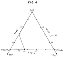
- the composition of the second ceramic oxide is chosen from within the triangular phase field defined by BaCuO2, CuO, and YBa2Cu3O7 of the ternary phase diagram 45 as shown in Figure 4.
- the second ceramic oxide has a composition approximately on a line in the ternary phase diagram of Figure 4 connecting (BaO) .3 (CuO) .7 on the BaO-CuO edge and the YBa2Cu3O7 compound.
- Specific compositions of the second ceramic oxide materials suitable are Y 0.062 Ba 0.28 Cu 0.72 O x , Y 0.068 Ba 0.28 Cu 0.72 O x , and Y 0.026 Ba 0.29 Cu 0.71 O x .
- Other second ceramic oxide materials may be used.
- FIG. 5 illustrates the preferred heat treating process 50 as applied to the composite structure which includes the 123 superconducting ceramic oxide, YBa2Cu3O 7-x .
- the first step 52 of the preferred heat treating process 50 involves heating the composite structure in a furnace to a temperature approximately in the range 970-995°C. That temperature range is lower than the incongruent melting point of the 123 superconductor at about 1030°C. The temperature is above the melting point of the second ceramic oxide, however, to dissolve either an adequate amount of, or the entire, 123 superconductor layer. The temperature is then either reduced immediately to about 930°C or held at temperature for about one hour before starting the cooling cycle. The cooling to 930°C may be at a rate between about 10 to 60°C per hour or, preferably, a more rapid thermal anneal may be used. The texturing treatment of the present invention is not, however, a sensitive function of the cooling rate. After reaching 930°C, the composite structure is either taken out of the furnace or given the anneal in oxygen required to produce a superconductor having a high critical temperature.
- One combination is to hold the composite structure in the furnace for about an hour at a temperature approximately in the range 970-995°C, step 60 ; reduce the temperature to about 930°C, step 62 ; then remove the composite structure from the furnace and cool the structure to room temperature, step 64 .
- a second combination is to hold the composite structure in the furnace for about an hour at a temperature approximately in the range 970-995°C, step 70 ; reduce the temperature to about 930°C, step 72 ; then anneal the structure, step 74 .
- a third combination involves reducing the temperature from the range 970-995°C to about 930°C without first holding the composite structure in the furnace for about an hour at a temperature approximately in the range 970-995°C, step 80 , then removing the composite structure from the furnace and cooling the structure to room temperature, step 82 .
- a fourth combination is reducing the temperature from the range 970-995°C to about 930°C without first holding the composite structure in the furnace for about an hour at a temperature approximately in the range 970-995°C, step 90 , then annealing the structure, step 92 .
- the annealing steps 74 and 92 described above are performed in oxygen gas and involve rapidly cooling the composite structure from the temperature of about 930°C to about 700°C, then slowly cooling the composite structure to room temperature.
- the superconducting, orthorhombic phase YBa2Cu3O 7-x (0 ⁇ x ⁇ 0.5) is produced by oxidation of the oxygen-deficient, tetragonal phase YBa2Cu3O 6+x (0 ⁇ x ⁇ 0.5) as the material is cooled through the tetragonal-to-orthorhombic transition.
- Performing the annealing steps 74 and 92 in oxygen allows formation of a material with uniform oxygen concentration. Accordingly, it is preferred that these steps be performed.
- heat treatments are described above as applied in a furnace or oven, they may also be accomplished in other modes of heating.
- alternative modes are infared radiation, electron beam pulse, or laser pulse.
- coatings of the 123 superconductor may or may not exhibit a highly crystalline, well-developed crystal x-ray diffraction pattern.
- the x-ray diffraction pattern obtained is that typical of a random array of 123 superconductor crystals, regardless of the initial degree of crystallization.
- the films are polycrystalline.
- Figure 6 depicts such a typical pattern, with several of the diffraction lines labeled.
- Figure 7 indicates the x- ray diffraction pattern of an oriented YBa2Cu3O7 film after processing according to the present invention. That pattern shows strong (00l) reflections of YBa2Cu3O7, most of which are more intense than the strongest line (103,110) in a pattern from randomly oriented YBa2Cu3O7 ( Figure 6).
- the degree of c-axis orientation can be estimated by comparing the sum of intensities of the (00l) reflections with the sum of all the other reflections (hkl) in the x-ray diffraction pattern.
- the (00l)/(hkl) ratio is approximately 0.15/1.0 ( Figure 6).
- the ratio is approximately 30/1.0, showing a 200-fold enhancement of c-axis orientation over a random sample. This demonstrates a preponderance of crystallites having their c-axes oriented near the film normal.
- Figure 9 is the ⁇ -2 ⁇ x-ray diffraction pattern for the film whose pole figure is shown in Figure 8.
- the oriented result can be explained by considering the possible mechanisms driving the growth of the 123 superconductor crystals in the composite structure during heat treatment.
- the growth of the highly crystalline 123 superconductor film begins with growth from the melt.
- a large degree of melting at temperatures below the peritectic temperature (about 1030°C) is obtained by preparing a bilayer structure with a Ba/Y ratio in the range between five and ten. From that bilayer structure, the YBa2Cu3O7 is transported into the multiphase, lower melting point, liquid mixture.
- the YBa2Cu3O7 is then precipitated out on the surface of that liquid as cooling occurs.
- the YBa2Cu3O7 phase comprises less than 50% of the overall film volume, the phase crystallizes in a layer above the melt because it has a lower density, because the surface is at a lower temperature, or both.
- the c-axis orientation is believed to be controlled by anisotropy in the kinetics of atomic attachment and in the energetics during growth.
- the direction parallel to the c-axis of the structure where "c" is the longest unit cell dimension (the vertical direction in Figure 10) appears to be the slowest growing.
- This phenomenon results in films with c-axis orientation having individual crystals where the ratio of the dimensions of the crystals parallel to the unit cell vectors "a" and "c", respectively, varies from three to over one hundred (the a-b plane is horizontal in Figure 10).
- growth kinetics contributes to the orientation of the YBa2Cu3O7 crystallites.
- the desired orientation shows alignment of the YBa2Cu3O7 grains, with the a-b planes of the orthorhombic crystal lattice (see Figure 11) lying parallel to each other and to the substrate surface.
- This orientation contains CuO2 planes parallel to the substrate surface which provide the pathways for carrying the current and give the oriented material a relatively high critical current density.
- the alignment is beneficial in resolving anisotropic thermal contraction and microcracking.
Landscapes
- Engineering & Computer Science (AREA)
- Manufacturing & Machinery (AREA)
- Superconductors And Manufacturing Methods Therefor (AREA)
- Inorganic Compounds Of Heavy Metals (AREA)
- Compositions Of Oxide Ceramics (AREA)
- Oxygen, Ozone, And Oxides In General (AREA)
- Crystals, And After-Treatments Of Crystals (AREA)
Claims (20)
- Verfahren zum Herstellen eines orientierten, supraleitenden keramischen Oxids aus einer Zweischichtstruktur aus einem polykristallinen supraleitenden keramischen Oxid und einem zweiten keramischen Oxidmaterial mit einem niedrigeren Schmelzpunkt als jenem des supraleitenden keramischen Oxides, das folgende Schritte beinhaltet:(a) Herstellen (32) eines im wesentlichen glatten Substrates;(b) Bilden (34, 36, 38, 40) einer Zweischichtstruktur mit einer polykristallinen supraleitenden keramischen Oxidschicht und einer zweiten keramischen Oxidschicht, die durch aufeinanderfolgende Deposition nacheinander auf dem Substrat angeordnet werden, wobei die zweite keramische Oxidschicht eine Dicke aufweist, die das Ein- bis Dreifache der Dicke des supraleitenden keramischen Oxidfilms beträgt; und(c) Wärmebehandeln (42) der zusammengesetzten Struktur aus Substrat und Zweischichtstruktur, um eine orientierte Struktur zu erzielen, bei der die c-Achsen der Einheitszellen der Kristallite überwiegend senkrecht zur Oberfläche des Substrates sind.
- Verfahren nach Anspruch 1, das des weiteren den Schritt zum Aufbringen einer zweiten supraleitenden keramischen Oxidschicht auf der orientierten Struktur beinhaltet.
- Verfahren nach Anspruch 1, wobei der Schritt des Wärmebehandelns der zusammengesetzten Struktur des weiteren ein Ätzen der auf dem Substrat aufgebrachten Zweischichtstruktur, um eine Mehrzahl von Gittern in dieser Struktur zu generieren, ein Erzeugen einer Temperzone in der Zweischichtstruktur und ein Durchleiten der Temperzone durch die Gitter hindurch beinhaltet, um eine orientierte, einkristalline, supraleitende Schicht zu bilden.
- Verfahren nach Anspruch 1, wobei das supraleitende keramische Oxid direkt auf die Oberseite des Substrats aufgebracht wird (36) und das zweite keramische Oxidmaterial auf das supraleitende keramische Oxid aufgebracht wird (38).
- Verfahren nach Anspruch 1, wobei das zweite keramische Oxidmaterial direkt auf die Oberseite des Substrats aufgebracht wird (34) und das supraleitende keramische Oxid auf das zweite keramische Oxidmaterial aufgebracht wird (40).
- Verfahren nach Anspruch 1, wobei der Schritt zum Aufbringen des supraleitenden keramischen Oxides des weiteren das Aufbringen des supraleitenden keramischen Oxides als Film mit einer Dicke von etwa 25 Mikrometer (1 x 10⁻³ Zoll) beinhaltet.
- Verfahren nach Anspruch 1, wobei die Depositionsschritte des weiteren die Bildung von Schichten aus dem zweiten keramischen Oxidmaterial und dem supraleitenden keramischen Oxid durch Auswählen von Depositionsprozessen aus der Gruppe beinhaltet, die aus Plasmasprühen, Aufdampfen, Sputtern und Doppelionenstrahldeposition besteht.
- Verfahren nach Anspruch 1, wobei das zweite keramische Oxidmaterial eine Zusammensetzung aufweist, die jener des supraleitenden keramischen Oxides im wesentlichen ähnlich ist.
- Verfahren nach Anspruch 1, wobei das supraleitende keramische Oxid YBa₂Cu₃O7-x (0 < x < 0,5) ist.
- Verfahren nach Anspruch 9, wobei die Zusammensetzung des zweiten keramischen Oxidmaterials innerhalb des Zusammensetzungsdreiecks liegt, das durch BaCuO₂, CuO und YBa₂Cu₃O₇ des ternären Phasendiagramms definiert ist, wobei das zweite keramische Oxidmaterial bei der Temperatur des Tempervorgangs als Lösungsmittel für das supraleitende keramische Oxid YBa₂Cu₃O7-x (0 < x < 0,5) wirkt.
- Verfahren nach Anspruch 10, wobei das zweite keramische Oxidmaterial eine Zusammensetzung aufweist, die ungefähr auf einer Linie in dem ternären Phasendiagramm liegt, die (BaO)0,3(CuO)0,7 auf der BaO-CuO-Kante und die YBa₂Cu₃O₇-Verbindung verbindet.
- Verfahren nach Anspruch 9, wobei der Schritt des Wärmebe- handelns des weiteren ein schnelles thermisches Tempern beinhaltet.
- Verfahren nach Anspruch 9, wobei das Wärmebehandeln in Sauerstoff durchgeführt wird.
- Verfahren nach Anspruch 9, wobei der Schritt des Wärmebehandelns des weiteren die Erwärmung (52) in einem Ofen auf eine Temperatur beinhaltet, die ungefähr im Bereich von 970 °C bis 995 °C liegt.
- Verfahren nach Anspruch 14, wobei der Schritt des Wärmebehandelns des weiteren beinhaltet:(a) Belassen (60) der zusammengesetzten Struktur in dem Ofen für etwa eine Stunde bei einer Temperatur, die ungefähr im Bereich von 970 °C bis 995 °C liegt;(b) Verringern (62) der Temperatur auf etwa 930 °C;(c) Entnehmen (64) der zusammengesetzten Struktur aus dem Ofen und Abkühlen der zusammengesetzten Struktur auf Raumtemperatur.
- Verfahren nach Anspruch 14, wobei der Schritt des Wärmebehandelns der zusammengesetzten Struktur des weiteren beinhaltet:(a) Belassen (70) der zusammengesetzten Struktur in dem Ofen für etwa eine Stunde bei einer Temperatur, die ungefähr im Bereich von 970 °C bis 995 °C liegt;(b) Verringern (72) der Temperatur auf etwa 930 °C;(c) Tempern (74) der zusammengesetzten Struktur.
- Verfahren nach Anspruch 16, wobei der Schritt des Temperns der zusammengesetzten Struktur des weiteren ein schnelles Abkühlen der zusammengesetzten Struktur in Sauerstoff auf etwa 700 °C und dann ein langsames Abkühlen der zusammengesetzten Struktur auf Raumtemperatur beinhaltet.
- Verfahren nach Anspruch 14, wobei der Schritt des Wärmebehandelns der zusammengesetzten Struktur des weiteren beinhaltet:(a) Verringern (80) der Temperatur auf etwa 930 °C;(b) Entnehmen (82) der zusammengesetzten Struktur aus dem Ofen und Abkühlen der zusammengesetzten Struktur auf Raumtemperatur.
- Verfahren nach Anspruch 14, wobei der Schritt des Wärmebehandelns der zusammengesetzten Struktur des weiteren beinhaltet:(a) Verringern (90) der Temperatur auf etwa 930 °C;(b) Tempern (92) der zusammengesetzten Struktur.
- Verfahren nach Anspruch 19, wobei der Schritt des Temperns der zusammengesetzten Struktur des weiteren ein schnelles Abkühlen der zusammengesetzten Struktur in Sauerstoff auf etwa 700 °C und dann ein langsames Abkühlen der zusammengesetzten Struktur auf Raumtemperatur beinhaltet.
Applications Claiming Priority (2)
| Application Number | Priority Date | Filing Date | Title |
|---|---|---|---|
| US07/498,180 US5206213A (en) | 1990-03-23 | 1990-03-23 | Method of preparing oriented, polycrystalline superconducting ceramic oxides |
| US498180 | 1990-03-23 |
Publications (2)
| Publication Number | Publication Date |
|---|---|
| EP0447767A1 EP0447767A1 (de) | 1991-09-25 |
| EP0447767B1 true EP0447767B1 (de) | 1994-07-27 |
Family
ID=23979913
Family Applications (1)
| Application Number | Title | Priority Date | Filing Date |
|---|---|---|---|
| EP91101250A Expired - Lifetime EP0447767B1 (de) | 1990-03-23 | 1991-01-31 | Verfahren zum Herstellen orientierter polykristalliner supraleitender keramischer Oxide |
Country Status (4)
| Country | Link |
|---|---|
| US (1) | US5206213A (de) |
| EP (1) | EP0447767B1 (de) |
| JP (1) | JPH04214064A (de) |
| DE (1) | DE69103054T2 (de) |
Families Citing this family (18)
| Publication number | Priority date | Publication date | Assignee | Title |
|---|---|---|---|---|
| US5648114A (en) * | 1991-12-13 | 1997-07-15 | Symetrix Corporation | Chemical vapor deposition process for fabricating layered superlattice materials |
| DE4119707A1 (de) * | 1991-06-14 | 1992-12-17 | Siemens Ag | Verfahren zum herstellen eines hochtemperatur-supraleitenden bauteiles und hochtemperatur-supraleitendes bauteil |
| US5786304A (en) * | 1992-04-03 | 1998-07-28 | Nippon Steel Corporation | Joining product of oxide superconducting material and process for producing the same |
| JP3008970B2 (ja) * | 1993-07-27 | 2000-02-14 | 財団法人国際超電導産業技術研究センター | Y123型結晶構造を有する酸化物結晶膜 |
| US5650378A (en) * | 1992-10-02 | 1997-07-22 | Fujikura Ltd. | Method of making polycrystalline thin film and superconducting oxide body |
| EP0591588B1 (de) * | 1992-10-06 | 1999-03-24 | Fujikura Ltd. | Verfahren zum Herstellen einer polykristalliner Dünnschicht und supraleitender Oxidkörper |
| US5523284A (en) * | 1992-11-05 | 1996-06-04 | Alfred University | Process for preparing a bulk textured superconductive material |
| KR960000500B1 (ko) * | 1992-11-14 | 1996-01-08 | 한국과학기술원 | YBa₂Cu₃O_7-x 초전도체의 개선된 제조 방법 |
| DE69404189T2 (de) * | 1993-03-31 | 1998-01-08 | Texas Instruments Inc | Leicht donatoren-dotierte Elektroden für Materialien mit hoher dielektrischer Konstante |
| US6037313A (en) * | 1994-09-16 | 2000-03-14 | Sumitomo Electric Industries, Ltd. | Method and apparatus for depositing superconducting layer onto the substrate surface via off-axis laser ablation |
| US5504060A (en) * | 1995-01-12 | 1996-04-02 | University Of Chicago | Method for harvesting rare earth barium copper oxide single crystals |
| US5856204A (en) * | 1995-09-28 | 1999-01-05 | Matsushita Electric Industrial Co., Ltd. | Tunnel-type Josephson element and method for manufacturing the same |
| US5908813A (en) * | 1997-02-14 | 1999-06-01 | Micron Technology, Inc. | Method making integrated circuit metallization with superconductor BEOL wiring |
| JP3942264B2 (ja) * | 1998-03-11 | 2007-07-11 | 富士通株式会社 | 半導体基板上に形成されるインダクタンス素子 |
| US6899928B1 (en) * | 2002-07-29 | 2005-05-31 | The Regents Of The University Of California | Dual ion beam assisted deposition of biaxially textured template layers |
| DE102004040754A1 (de) * | 2004-08-23 | 2006-03-09 | Siemens Ag | Rechteckspule aus bandförmigen Supraleitern mit HochTc-Supraleitermaterial und Verwendung derselben |
| US8141769B2 (en) * | 2005-07-22 | 2012-03-27 | Siemens Aktiengesellschaft | Process for repairing a component comprising a directional microstructure by setting a temperature gradient during the laser heat action, and a component produced by such a process |
| CN110156494A (zh) * | 2019-06-17 | 2019-08-23 | 佛山市东鹏陶瓷有限公司 | 一种微晶复合板的制备方法 |
Family Cites Families (6)
| Publication number | Priority date | Publication date | Assignee | Title |
|---|---|---|---|---|
| JPS59102890A (ja) * | 1982-11-29 | 1984-06-14 | Canon Inc | 薄膜結晶成長法 |
| CA1326976C (en) * | 1987-05-26 | 1994-02-15 | Satoshi Takano | Superconducting member |
| NL8701788A (nl) * | 1987-07-29 | 1989-02-16 | Philips Nv | Werkwijze voor het vervaardigen van een supergeleidende dunne laag. |
| JPH01161628A (ja) * | 1987-12-17 | 1989-06-26 | Mitsubishi Electric Corp | 酸化物超電導薄膜作成法 |
| JPH01257107A (ja) * | 1988-04-07 | 1989-10-13 | Tokai Univ | 超電導材の製造方法 |
| EP0387525B1 (de) * | 1989-03-15 | 1993-08-11 | Asea Brown Boveri Ag | Verfahren zur Herstellung einer kristallorientierten Oberflächenschicht aus einem keramischen Hochtemperatur-Supraleiter |
-
1990
- 1990-03-23 US US07/498,180 patent/US5206213A/en not_active Expired - Lifetime
-
1991
- 1991-01-31 DE DE69103054T patent/DE69103054T2/de not_active Expired - Fee Related
- 1991-01-31 EP EP91101250A patent/EP0447767B1/de not_active Expired - Lifetime
- 1991-02-22 JP JP3048752A patent/JPH04214064A/ja active Pending
Also Published As
| Publication number | Publication date |
|---|---|
| DE69103054T2 (de) | 1995-03-09 |
| DE69103054D1 (de) | 1994-09-01 |
| US5206213A (en) | 1993-04-27 |
| EP0447767A1 (de) | 1991-09-25 |
| JPH04214064A (ja) | 1992-08-05 |
Similar Documents
| Publication | Publication Date | Title |
|---|---|---|
| EP0447767B1 (de) | Verfahren zum Herstellen orientierter polykristalliner supraleitender keramischer Oxide | |
| CA2029355C (en) | Compound oxide superconducting thin film with buffer layer | |
| EP0345441B1 (de) | Hochtemperatursupraleiter-Gallatkristallstruktur | |
| EP0406126B1 (de) | Substrat mit einer supraleitenden Schicht | |
| EP0298866A2 (de) | Supraleitende dünne Schicht und Verfahren zu ihrer Herstellung | |
| EP0327493B1 (de) | Epitaxische Anordnung von Hochtemperatur-Supraleitern | |
| US5179070A (en) | Semiconductor substrate having a superconducting thin film with a buffer layer in between | |
| Xu et al. | A review of coated conductor development | |
| EP0341148B1 (de) | Halbleitersubstrat mit dünner Supraleiterschicht | |
| EP0347336B1 (de) | Verfahren zur Abscheidung einer dünnen Supraleiterschicht | |
| Wasa et al. | Thin film processing for high-Tc superconductors of the Bi-system | |
| EP0973208B1 (de) | Vorrichtung mit Gitteranpassung und Verfahren zu ihrer Herstellung | |
| Ramesh et al. | Thin film Y Ba Cu O high Tc superconductors: structure-property relationships | |
| EP0366510B2 (de) | Verfahren zur Herstellung eines Oxidverbindungssupraleiters des Bi-Sr-Ca-Cu-Systems | |
| JP2501035B2 (ja) | 超電導薄膜 | |
| US5236894A (en) | Process for producing a superconducting thin film at relatively low temperature | |
| EP0431595B1 (de) | Dünnfilm aus supraleitendem Oxid | |
| EP0323342A2 (de) | Ein Halbleitersubstrat mit einem supraleitenden Dünnfilm | |
| Sathiraju et al. | Studies on Ba/sub 2/YNbO/sub 6/buffer layers for subsequent YBa/sub 2/Cu/sub 3/O/sub 7-x/film growth | |
| Xu | High J c Epitaxial YBa 2 Cu 3 O 7-δ Films Through a Non-Fluorine Approach for Coated Conductor Applications | |
| Chrisey | Progress in the first ten years of HTS film growth | |
| Kim et al. | Fabrication of NdGaO/sub 3/buffer layer on textured Ni tape for long length coated conductors | |
| Ichinose et al. | Microstructures of high-T/sub c/superconducting films having artificial pinning centers | |
| Kobayashi et al. | Chemi-physical diagnosis of BiSrCaCuO thin film preparation | |
| Humphreys | Ceramic superconductors |
Legal Events
| Date | Code | Title | Description |
|---|---|---|---|
| PUAI | Public reference made under article 153(3) epc to a published international application that has entered the european phase |
Free format text: ORIGINAL CODE: 0009012 |
|
| AK | Designated contracting states |
Kind code of ref document: A1 Designated state(s): DE FR GB |
|
| 17P | Request for examination filed |
Effective date: 19911219 |
|
| 17Q | First examination report despatched |
Effective date: 19930618 |
|
| GRAA | (expected) grant |
Free format text: ORIGINAL CODE: 0009210 |
|
| AK | Designated contracting states |
Kind code of ref document: B1 Designated state(s): DE FR GB |
|
| REF | Corresponds to: |
Ref document number: 69103054 Country of ref document: DE Date of ref document: 19940901 |
|
| ET | Fr: translation filed | ||
| PGFP | Annual fee paid to national office [announced via postgrant information from national office to epo] |
Ref country code: FR Payment date: 19941223 Year of fee payment: 5 |
|
| PGFP | Annual fee paid to national office [announced via postgrant information from national office to epo] |
Ref country code: DE Payment date: 19950117 Year of fee payment: 5 |
|
| PLBE | No opposition filed within time limit |
Free format text: ORIGINAL CODE: 0009261 |
|
| STAA | Information on the status of an ep patent application or granted ep patent |
Free format text: STATUS: NO OPPOSITION FILED WITHIN TIME LIMIT |
|
| 26N | No opposition filed | ||
| PGFP | Annual fee paid to national office [announced via postgrant information from national office to epo] |
Ref country code: GB Payment date: 19951215 Year of fee payment: 6 |
|
| PG25 | Lapsed in a contracting state [announced via postgrant information from national office to epo] |
Ref country code: FR Effective date: 19960930 |
|
| PG25 | Lapsed in a contracting state [announced via postgrant information from national office to epo] |
Ref country code: DE Effective date: 19961001 |
|
| REG | Reference to a national code |
Ref country code: FR Ref legal event code: ST |
|
| PG25 | Lapsed in a contracting state [announced via postgrant information from national office to epo] |
Ref country code: GB Effective date: 19970131 |
|
| GBPC | Gb: european patent ceased through non-payment of renewal fee |
Effective date: 19970131 |