EP0973208B1 - Vorrichtung mit Gitteranpassung und Verfahren zu ihrer Herstellung - Google Patents
Vorrichtung mit Gitteranpassung und Verfahren zu ihrer Herstellung Download PDFInfo
- Publication number
- EP0973208B1 EP0973208B1 EP99118017A EP99118017A EP0973208B1 EP 0973208 B1 EP0973208 B1 EP 0973208B1 EP 99118017 A EP99118017 A EP 99118017A EP 99118017 A EP99118017 A EP 99118017A EP 0973208 B1 EP0973208 B1 EP 0973208B1
- Authority
- EP
- European Patent Office
- Prior art keywords
- substrate
- thin film
- axis
- srtio
- yba
- Prior art date
- Legal status (The legal status is an assumption and is not a legal conclusion. Google has not performed a legal analysis and makes no representation as to the accuracy of the status listed.)
- Expired - Lifetime
Links
Images


Classifications
-
- H—ELECTRICITY
- H10—SEMICONDUCTOR DEVICES; ELECTRIC SOLID-STATE DEVICES NOT OTHERWISE PROVIDED FOR
- H10N—ELECTRIC SOLID-STATE DEVICES NOT OTHERWISE PROVIDED FOR
- H10N60/00—Superconducting devices
- H10N60/01—Manufacture or treatment
- H10N60/0268—Manufacture or treatment of devices comprising copper oxide
- H10N60/0296—Processes for depositing or forming copper oxide superconductor layers
- H10N60/0576—Processes for depositing or forming copper oxide superconductor layers characterised by the substrate
- H10N60/0632—Intermediate layers, e.g. for growth control
-
- H—ELECTRICITY
- H10—SEMICONDUCTOR DEVICES; ELECTRIC SOLID-STATE DEVICES NOT OTHERWISE PROVIDED FOR
- H10N—ELECTRIC SOLID-STATE DEVICES NOT OTHERWISE PROVIDED FOR
- H10N60/00—Superconducting devices
- H10N60/01—Manufacture or treatment
- H10N60/0268—Manufacture or treatment of devices comprising copper oxide
- H10N60/0661—Processes performed after copper oxide formation, e.g. patterning
-
- H—ELECTRICITY
- H10—SEMICONDUCTOR DEVICES; ELECTRIC SOLID-STATE DEVICES NOT OTHERWISE PROVIDED FOR
- H10N—ELECTRIC SOLID-STATE DEVICES NOT OTHERWISE PROVIDED FOR
- H10N60/00—Superconducting devices
- H10N60/01—Manufacture or treatment
- H10N60/0912—Manufacture or treatment of Josephson-effect devices
- H10N60/0941—Manufacture or treatment of Josephson-effect devices comprising high-Tc ceramic materials
-
- H—ELECTRICITY
- H10—SEMICONDUCTOR DEVICES; ELECTRIC SOLID-STATE DEVICES NOT OTHERWISE PROVIDED FOR
- H10N—ELECTRIC SOLID-STATE DEVICES NOT OTHERWISE PROVIDED FOR
- H10N60/00—Superconducting devices
- H10N60/10—Junction-based devices
-
- H—ELECTRICITY
- H10—SEMICONDUCTOR DEVICES; ELECTRIC SOLID-STATE DEVICES NOT OTHERWISE PROVIDED FOR
- H10N—ELECTRIC SOLID-STATE DEVICES NOT OTHERWISE PROVIDED FOR
- H10N60/00—Superconducting devices
- H10N60/10—Junction-based devices
- H10N60/12—Josephson-effect devices
- H10N60/124—Josephson-effect devices comprising high-Tc ceramic materials
-
- Y—GENERAL TAGGING OF NEW TECHNOLOGICAL DEVELOPMENTS; GENERAL TAGGING OF CROSS-SECTIONAL TECHNOLOGIES SPANNING OVER SEVERAL SECTIONS OF THE IPC; TECHNICAL SUBJECTS COVERED BY FORMER USPC CROSS-REFERENCE ART COLLECTIONS [XRACs] AND DIGESTS
- Y10—TECHNICAL SUBJECTS COVERED BY FORMER USPC
- Y10S—TECHNICAL SUBJECTS COVERED BY FORMER USPC CROSS-REFERENCE ART COLLECTIONS [XRACs] AND DIGESTS
- Y10S505/00—Superconductor technology: apparatus, material, process
- Y10S505/70—High TC, above 30 k, superconducting device, article, or structured stock
- Y10S505/701—Coated or thin film device, i.e. active or passive
- Y10S505/702—Josephson junction present
-
- Y—GENERAL TAGGING OF NEW TECHNOLOGICAL DEVELOPMENTS; GENERAL TAGGING OF CROSS-SECTIONAL TECHNOLOGIES SPANNING OVER SEVERAL SECTIONS OF THE IPC; TECHNICAL SUBJECTS COVERED BY FORMER USPC CROSS-REFERENCE ART COLLECTIONS [XRACs] AND DIGESTS
- Y10—TECHNICAL SUBJECTS COVERED BY FORMER USPC
- Y10S—TECHNICAL SUBJECTS COVERED BY FORMER USPC CROSS-REFERENCE ART COLLECTIONS [XRACs] AND DIGESTS
- Y10S505/00—Superconductor technology: apparatus, material, process
- Y10S505/70—High TC, above 30 k, superconducting device, article, or structured stock
- Y10S505/704—Wire, fiber, or cable
-
- Y—GENERAL TAGGING OF NEW TECHNOLOGICAL DEVELOPMENTS; GENERAL TAGGING OF CROSS-SECTIONAL TECHNOLOGIES SPANNING OVER SEVERAL SECTIONS OF THE IPC; TECHNICAL SUBJECTS COVERED BY FORMER USPC CROSS-REFERENCE ART COLLECTIONS [XRACs] AND DIGESTS
- Y10—TECHNICAL SUBJECTS COVERED BY FORMER USPC
- Y10S—TECHNICAL SUBJECTS COVERED BY FORMER USPC CROSS-REFERENCE ART COLLECTIONS [XRACs] AND DIGESTS
- Y10S505/00—Superconductor technology: apparatus, material, process
- Y10S505/725—Process of making or treating high tc, above 30 k, superconducting shaped material, article, or device
- Y10S505/729—Growing single crystal, e.g. epitaxy, bulk
Definitions
- the present invention relates to a superconducting thin film grain boundary junction device and a method for fabricating such device.
- La 2-x M x CuO 4-y (M: Sr, Ba, 0 ⁇ x ⁇ 1) discovered in 1986 has a superconductivity transition temperature (T c ) of 30-40K which is much higher than the T c of conventional metal superconductor and, hence, extensive research on oxide superconductors has been made.
- T c superconductivity transition temperature
- LnBa 2 Cu 3 O x (Ln: Y or lanthanides; 6 ⁇ x ⁇ 7) oxide superconductors having T c of about 90K, BiSrCaCuO x oxide superconductors having T c of about 110K, and TlBaCaCuO x oxide superconductors having T c of about 120K have been discovered one after another.
- junction devices which utilize, among these high temperature superconductors, YBa 2 Cu 3 O x . These junction devices are classified into two groups, one is a group of vertical junction devices and the other is a group of lateral junction devices.
- the lateral junction devices include (1) a junction using a so-called bicrystal substrate which has two substrate regions adjacent each other differing in the direction of crystal axis from each other, and (2) a 45°-inclined junction having a first thin film formed on SrTiO 3 and a second thin film formed on MgO in which the first and second thin films have different intraplanar directions from each other.
- Fig. 1A is a planar view showing a thin film
- Fig. 1B is a cross sectional view showing the thin film shown in Fig. 1A.
- reference numerals 31, 31' are SrTiO 3 substrates, respectively.
- the SrTiO 3 substrates 31 and 31' have different directions of crystal axes.
- Reference numeral 38 designates a junction portion at which the SrTiO 3 substrates 31 and 31', differing in the direction of crystal axis one from another, are adjacent to each other.
- Reference numerals 33 and 33' are YBa 2 Cu 3 O x thin films, respectively, formed on the bicrystal substrate.
- Arrows c indicate the direction of c-axes of the thin films 33, 33', and arrows a/b indicate directions of a- or b-axes of the thin films 33 and 33'.
- Reference numeral 35 designates an inclined grain boundary junction.
- CuO 2 planes (a- or b-planes), in which electric current flows, exist in the same plane in both electrodes that sandwich the junction and contact each other in parallel relation. In this arrangement, leak current increases.
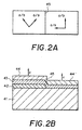
- Fig. 2A is a planar view showing a conventional thin film
- Fig. 2B is a cross sectional view showing the thin film shown in Fig. 2A
- reference numeral 41 designates a sapphire substrate
- 42 is a MgO thin film formed on a part of a surface of the sapphire substrate 41
- 43 is a SrTiO 3 thin film over the MgO thin film 42 and the remaining part of the surface of the sapphire substrate 41
- 44 and 44' are c-axis oriented YBa 2 Cu 3 O x thin films, respectively, formed on the SrTiO 3 thin film 43.
- Reference numeral 45 designates a grain boundary junction formed between the thin films 44 and 44'.
- Arrows c indicate the direction of c-axes of the YBa 2 Cu 3 O x thin films 44 and 44', and arrows a/b indicate the direction of a- or b-axes of the YBa 2 Cu 3 O x thin films 44 and 44', respectively.
- the axes of preferential orientation of the electrodes sandwiching the grain boundary junction 45 are the same as the c-axis while the YBa 2 Cu 3 O x thin films 44 and 44' form a 45°-inclined junction.
- CuO 2 planes (a- or b-planes), in which electric current flows, exist in the same plane in both electrodes sandwiching the junction and contact each other in parallel relation, as in the case of the bicrystal.
- the CuO 2 planes in the YBa 2 Cu 3 O x in which electric current flows, always exist in the planes of YBa 2 Cu 3 O x thin films 44 and 44', and the CuO 2 planes contact each other always in parallel (a/b-axis direction vs. a/b-axis direction) in a boundary region of the junction and in the both electrode portions.
- This arrangement causes a serious problem of increase in leak current.
- superconducting current flows in c-axis direction having a small coherence length at a critical current density by several digits smaller than a-axis direction having a large coherence length.
- superconducting current must flow through a c-axis oriented portion having a small coherence length at the time of transmission and receipt of signals from a lower circuit layer to an upper circuit layer.
- cross section must be large so that the density of signal current does not exceed a critical current density. This causes a problem of difficulty of high integration of circuits.
- EP-A-05 02 787 relates to a thin film of oxide superconductor consisting of more than two portions each possessing a predetennined crystal orientation and deposited on a common surface of a substrate. At least one selected portion of the thin film of oxide superconductor is deposited on a thin under-layer which facilitates crystal growth of the selected portion and which is deposited previously on the substrate.
- the selected portions may consist of a-axis oriented thin film portions while non-selected portions may consists of c-axis oriented thin film portions.
- the thin under-layer can be a buffer layer or a very thin film of oxide superconductor. MgO substrates for a-axis oriented portions and PrGaO 3 thin under-layers for c-axis oriented portions are proposed.
- An object of the present invention is to provide a superconducting thin film device in which a desired region on a substrate has a desired preferential orientation and a method for fabricating such a device.
- Another object of the present invention is to provide a superconducting thin film grain boundary junction device including a substrate having formed thereon a grain boundary junction whose CuO 2 planes in which current flows cross at right angles each other and showing less leak current, and a method for fabricating such a device.
- the present invention provides a superconducting thin film grain boundary junction device comprising: a substrate; first and second monocrystal regions provided on the substrate and having lattice mismatches with respect to a superconductor represented by formula LnBa 2 Cu 3 O x wherein Ln represents yttrium or a lanthanide, and x satisfies 6 ⁇ x ⁇ 7, wherein the lattice mismatch of said first monocrystal region is exceeding 1% and the lattice mismatch of said second monocrystal region is not exceeding 1%; a superconducting thin film composed of a superconductor represented by formula LnBa 2 Cu 3 O x wherein Ln represents yttrium or a lanthanide, and x satisfies 6 ⁇ x ⁇ 7, the superconducting thin film in said first monocrystal region having a c-axis perpendicular to a surface of the superconducting thin film, and said superconducting thin film in said second
- the substrate may consist of a material selected from the group consisting of Nd:YAlO 3 , LaAlO 3 , SrLaGaO 4 , NdGaO 3 , PrGaO 3 , LaGaO 3 , SrTiO 3 and MgO.
- the present invention also provides a method for fabricating a lattice matching device, comprising the steps of: providing a substrate; forming on a surface of the substrate at least two monocrystal regions having lattice mismatches with respect to a superconductor represented by a formula LnBa 2 Cu 3 O x wherein Ln represents yttrium or a lanthanide, and x satisfies 6 ⁇ x ⁇ 7, wherein the lattice mismatches of some of said at least two regions are exceeding 1% and the lattice mismatches of others of said at least two monocrystal regions are not exceeding 1%; simultaneously forming on said first and second monocrystal regions a thin film of a superconductor represented by a formula LnBa 2 Cu 3 O x wherein Ln represents yttrium or a lanthanide, and x satisfies 6 ⁇ x ⁇ 7, at a substrate temperature from 550 to 850°C and an oxygen pressure from 1,
- the substrate may consist of a material selected from the group consisting of Nd:YAlO 3 , LaAlO 3 , SrLaGaO 4 , NdGaO 3 , PrGaO 3 , LaGaO 3 , SrTiO 3 and MgO.
- a grain boundary junction whose CuO 2 planes in that superconducting current flows contact perpendicular to each other can be fabricated with ease in high yield, the junction showing less leak current.
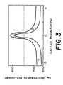
- Fig. 3 is a graph illustrating dependence of an axis of crystallographic orientation on substrate temperature when a thin film of a YBa 2 Cu 3 O x superconductor is formed on a substrate composed of a material having a lattice mismatch differing from that of the YBa 2 Cu 3 O x superconductor, the substrate being composed of a metal oxide such as MgO, SrTiO 3 , LaSrGaO 4 , PrGaO 3 , NdGaO 3 , LaAlO 3 , or YAlO 3 .
- a metal oxide such as MgO, SrTiO 3 , LaSrGaO 4 , PrGaO 3 , NdGaO 3 , LaAlO 3 , or YAlO 3 .
- a substrate temperature or deposition temperature exists at which there appear both a-axis oriented and c-axis oriented phases.
- Table 1 below shows lattice constant at room temperature, lattice constant of pseudo tetragonal crystal, crystal structure, and thermal expansion coefficient of various substrates.
- the substrate materials have different lattice mismatches with respect to YBa 2 Cu 3 O x from each other.
- symbol a designates a region where a YBa 2 Cu 3 O x thin film grows which has an a-axis orientation (i.e., a CuO 2 plane is perpendicular to a surface of the substrate);
- symbol c designates a region where a YBa 2 Cu 3 O x thin film grows which has a c-axis orientation (i.e., a CuO 2 plane is parallel to a surface of the substrate);
- symbol (a+c) designates a region where a YBa 2 Cu 3 O x thin film in which a-axis orientation and c-axis orientation coexist.
- Fig. 3 indicates that crystal directions (orientations) of YBa 2 Cu 3 O x superconducting thin films formed on substrates composed of different materials, respectively, depend on lattice mismatch with respect to the materials of substrates even when the substrates are at the same substrate temperature.
- a YBa 2 Cu 3 O x superconducting thin film is c-axis oriented on a substrate composed of a material having a large lattice mismatch with respect to the thin film while it is a-axis oriented on a substrate composed of a material having a small lattice mismatch with respect to the thin film.
- a YBa 2 Cu 3 O x thin film deposited on SrTiO 3 has a c-axis orientation (i.e., CuO 2 plane is parallel to a surface of the substrate) while a YBa 2 Cu 3 O x thin film deposited on PrGaO 3 has an a-axis orientation (CuO 2 plane is perpendicular to a surface of the substrate). Therefore, the CuO 2 plane in which current flows can be made perpendicular to a surface of the thin film to thereby reduce leak current, which was impossible to attain conventionally.
- Fabrication of thin films can be performed by laser beam vapor deposition, for example, ArF excimer laser beam vapor deposition.
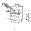
- Laser beam vapor deposition can be carried out by using a conventional laser beam vapor deposition apparatus as shown in Fig. 4.
- reference numeral 50 designates a laser beam vapor deposition apparatus, which is provided with a vacuum container 52 formed with an inlet window 54. Inside the vacuum container 52, there is fixed a support rod 56. To a top 56a of the support rod 56 is attached a substrate holder 58 on which a substrate 59 is mounted. Opposite to the substrate holder 58, there is arranged a target holder 60 on which a target 61 is held. A motor 62 is arranged outside the vacuum container 52.
- the motor 62 has a shaft 64, which is inserted into the vacuum container 52 airtightly. An end of the shaft 64 is connected to the target holder 60, and the target holder 60 is rotated by the shaft 64 driven by the motor 62.
- the vacuum container 52 is connected to an oxygen inlet conduit 70 which supplies oxygen to the vacuum container 52 through a leak valve 68.
- the vacuum container 52 is provided with an exhaust port 72 and a valve 74 through which the vacuum container 52 is connected to an exhaust system (not shown) to maintain vacuum. Outside the inlet window 54, there is arranged a focusing lens 78 and a laser beam source (not shown).
- a laser beam from the laser beam source (not shown) passes through the focusing lens 78 and then through the inlet window 54 arrives onto a rotating target driven by the shaft 64 of the motor 62 to generate plasma, and allows a thin film to deposit on an opposing substrate held on the substrate holder 58.
- the substrate attached to the substrate holder 58 heated by a heater (not shown) energized by a power source (not shown) for the heater to an appropriate temperature.
- the temperature is monitored by a thermocouple (not shown).
- a vacuum meter 80 attached to the vacuum container 52 monitors degree of vacuum inside the vacuum container 52 and sends a control signal to a vacuum control system (not shown) for adjusting the vacuum degree.
- oxygen source there can be used oxygen atom, or ozone. Generally, it is carried out at a substrate temperature of from 550 to 850°C, preferably from 600 to 750°C, at an oxygen pressure of from 1,33 x 10 -8 from (1x10 -5 ) Torr to 1,33 x 10 -2 bar (10 Torr), preferably from 1,33 x 10 -6 bar (1 mTorr) to 1,33 x 10 -3 bar (1 Torr).
- the substrate is composed of (100) SrTiO 3 having a lattice mismatch of 1.1%, a part of which is masked with MgO and unmasked part of which is deposited with a PrGaO 3 thin film having a lattice mismatch of 0.02% at a substrate temperature of 750°C and at an oxygen pressure of 50 mTorr to a thickness of 50 ⁇ .
- the mask is removed and a YBa 2 Cu 3 O x thin film is deposited to a thickness of 800 ⁇ at a substrate temperature of 680°C and at an oxygen pressure of 5,32 x 10 -4 bar (400 mTorr).
- the thin film formed can be evaluated by XRD, RHEED, ⁇ -scan using a (102) surface, and cross section TEM.
- Orientation axis length of the YBa 2 Cu 3 O x thin film formed is measured by X-ray diffraction (XRD) analysis using Cu-K ⁇ .
- Preferential orientation axis of the YBa 2 Cu 3 O x is determined by the intensities obtained by XRD. That is, c-axis and a-axis orientations are assumed to be represented by (005) peak and (200) peak, respectively, of the YBa 2 Cu 3 O x as representative peaks, and when both (005) and (200) peaks are detected by XRD, then the stronger peak is judged to be dominant, and when one of them is undetectable at all, orientation is judged to be pure or uniform.
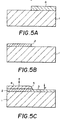
- Figs. 5A, 5B and 5C are cross sectional views illustrating fabrication of a grain boundary junction device according to a first example of the present invention.
- reference numeral 1 designates a SrTiO 3 substrate
- 2 is a PrGaO 3 layer
- 3 is a c-axis oriented YBa 2 Cu 3 O x thin film
- 4 is an a-axis oriented YBa 2 Cu 3 O x thin film
- 5 is a grain boundary junction formed between the c-axis oriented YBa 2 Cu 3 O x thin film 3 and the a-axis oriented YBa 2 Cu 3 O x thin film 4
- 6 is a mask.
- Fig. 5A shows, in cross section, a SrTiO 3 substrate 1 having a lattice mismatch with respect to YBa 2 Cu 3 O x of 1.1%, for example, the substrate having thereon a mask 6. Then, PrGaO 3 having a lattice mismatch with respect to YBa 2 Cu 3 O x of 0.02% is deposited on a part of the surface of the substrate 1 which part is uncovered by the mask 6. Removal of the mask 6 gives a structure shown in Fig. 5B.
- a YBa 2 Cu 3 O x thin film is deposited on overall surface of the substrate shown in Fig. 5B at a substrate temperature of 750°C which is shown in broken line in Fig. 3. As shown in Fig. 5C, a YBa 2 Cu 3 O x thin film is deposited on overall surface of the substrate shown in Fig. 5B at a substrate temperature of 750°C which is shown in broken line in Fig. 3. As shown in Fig.
- the grain boundary junction 5 is a grain boundary junction of c-axis orientation/a-axis orientation in which a CuO 2 plane, that allows current to pass therein, crosses the boundary portion between the both YBa 2 Cu 3 O x thin films at right angles.
- a grain boundary junction according to a second example of the present invention will be described below.
- This example uses a (110) PrGaO 3 substrate and a SrTiO 3 deposition material.
- Fig. 6A is a planar view showing a grain boundary junction according to this example
- Fig. 6B is a cross sectional view of the grain boundary junction shown in Fig. 6A.
- Fig. 6A is a planar view showing a grain boundary junction according to this example
- Fig. 6B is a cross sectional view of the grain boundary junction shown in Fig. 6A.
- reference numeral 2 designates a (110) PrGaO 3 substrate
- 1 is SrTiO 3 layer deposited on the substrate 2
- 3 is a c-axis oriented YBa 2 Cu 3 O x thin film
- 4 is an a-axis oriented YBa 2 Cu 3 O x thin film
- 5 is a grain boundary junction formed between the c-axis oriented YBa 2 Cu 3 O x thin film 3 and the a-axis oriented YBa 2 Cu 3 O x thin film 4
- 7 is an arrow indicating direction of longer axis in an in-plane lattice of the substrate.
- Fabrication of the grain boundary junction device of this example is in substantially the same manner as in Example 1 illustrated in Figs. 5A to 5C except that a portion designed to be a-axis oriented must be masked.
- a material whose in-plane lattice is not square such as (110) PrGaO 3 , (110) NdGaO 3 , or (100) LaSrGaO 4
- the resulting a-axis oriented YBa 2 Cu 3 O x thin film has a c-axis which is parallel to a surface of the substrate is in its nature in the direction of the longer axis of the in-plane lattice of the substrate.
- the junction plane is defined between an a-/b-axis oriented YBa 2 Cu 3 O x thin film (formed on the SrTiO 3 layer) and a c-axis oriented YBa 2 Cu 3 O x thin film (formed on the PrGaO 3 substrate).
- a junction which has a junction plane defined between an a-/b-axis oriented YBa 2 Cu 3 O x thin film (formed on the SrTiO 3 layer) and a b-axis oriented YBa 2 Cu 3 O x thin film (formed on the PrGaO 3 substrate), which plane is perpendicular to a CuO 2 plane, that allows current to flow therein.
- the junction plane of a grain boundary junction can be controlled by selecting orientation of the crystal of the substrate.
- the junction is fabricated only one side of the original substrate.
- an unmasked portion may be formed in the form of a rectangle on the substrate so that a plurality of junctions can be fabricated.
- a junction between a-/b-axis oriented thin film and a c-axis oriented thin film is fabricated on side of the rectangle and a junction between an a-/b-axis oriented thin film and a b-axis oriented thin film is fabricated on another side of the rectangle, thus giving rise to a junction having opposing electrodes one of which is constituted by an a-axis oriented thin film and the other is constituted by a c-axis oriented thin film so that a CuO 2 plane in which current flows can be perpendicular to a surface of the substrate.
- different types of junctions can be fabricated at will by selecting preferential orientation of the substrate.
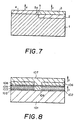
- Fig. 7 is a cross sectional view showing a grain boundary junction according to a third example of the present invention.
- reference numeral 1 designates SrTiO 3 layer
- 2 is a (110) PrGaO 3 substrate
- 3 is a c-axis oriented YBa 2 Cu 3 O x thin film
- 4 is an a-axis oriented YBa 2 Cu 3 O x thin film
- 5 is a grain boundary junction.
- the grain boundary junction device according to this example is fabricated in the same manner as the grain boundary junction device shown in Fig. 6B except that after a mask is provided on the substrate as shown in Figs.
- the substrate is etched to some depth, and SrTiO 3 is deposited on the etched portion to form a SrTiO 3 layer 1 to make up the hollow portion or provide an even or leveled surface.
- the leveling is advantageous in that a junction having a uniform junction plane 5a free of irregular crystal orientation.
- the both regions may be formed by deposition of thin films. In that case, less expensive substrates may be used.
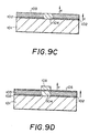
- Fig. 8 is a cross sectional view showing a superconducting vertical junction according to a fourth example.
- reference numeral 101 is a NdGaO 3 substrate
- 102 is a SrTiO 3 thin film
- 103 is a lower electrode composed of a c-axis oriented YBa 2 Cu 3 O x thin film
- 104 is a lower electrode composed of an a-axis oriented YBa 2 Cu 3 O x thin film
- 105 is a barrier layer composed of a SrTiO 3 thin film
- 106 is a SrTiO 3 interlayer insulator
- 107 is an upper electrode composed of a c-axis oriented YBa 2 Cu 3 O x thin film.
- the junction portion is comprised by the upper electrode 107, the barrier layer 105 and the lower electrode 104 which constitute a superconductor/insulator/superconductor structure (SIS structure).
- the superconducting wiring 103 is composed of a c-axis oriented thin film (i.e., a thin film whose c-axis in the direction of a smaller coherence length is perpendicular to a surface of the substrate) and the lower electrode 104 is composed of an a-axis oriented thin film (i.e., a thin film whose c-axis in the direction of a smaller coherence length is in a plane parallel to a surface of the substrate).
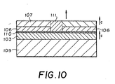
- FIG. 9A illustrates a state in which a mask 108 is formed on, for example, a NdGaO 3 substrate 101 having a lattice mismatch with respect to YBa 2 Cu 3 O x of 0.3%. Then, for example, a SrTiO 3 layer 102 having a lattice mismatch with respect to YBa 2 Cu 3 O x of 1.1% is deposited on a portion other than that covered with the mask 108. After the deposition, the mask 108 is removed.
- Fig. 9B shows an arrangement in which the mask 108 has been removed after the deposition of the SrTiO 3 layer 102.
- a YBa 2 Cu 3 O x thin film On the overall surface of the substrate, there is deposited a YBa 2 Cu 3 O x thin film at a substrate temperature of 750°C, for example, which is shown in broken line in Fig. 3.
- a c-axis oriented YBa 2 Cu 3 O x thin film 103 is deposited on the SrTiO 3 thin film 102 and an a-axis oriented YBa 2 Cu 3 O x thin film 104 is deposited on the NdGaO 3 substrate 101, as shown in Fig. 9C.
- a SrTiO 3 ultra thin film 105 serving as a barrier layer, followed by depositing a mask 108 on the a-axis oriented YBa 2 Cu 3 O x thin film 104 which constitutes a superconducting junction to obtain a structure as shown in Fig. 9D.
- a SrTiO 3 interlayer insulator 106 is deposited on the surface of the structure shown in Fig. 9D, and after the mask 108 is removed, an upper electrode 107 is deposited to obtain an arrangement shown in Fig. 8.
- the c-axis oriented thin film 103 having the a-axis oriented lower electrode 104 only on the junction portion. While explanation has been made hereinabove on the case where a c-axis oriented thin film is used as the upper electrode, there may be used those thin films oriented in directions other than the direction of c-axis (such as ⁇ 103>, ⁇ 110>, ⁇ 100>, etc.). Needless to say, the effect of the present invention can be obtained if only an a-axis oriented lower electrode exists only on the junction portion.
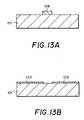
- Fig. 10 is a cross sectional view showing a superconducting vertical junction according to a fifth example.
- reference numeral 103 designates a lower electrode composed of a c-axis oriented YBa 2 Cu 3 O x thin film
- 106 is a SrTiO 3 interlayer insulator
- 107 is an upper electrode composed of a c-axis oriented YBa 2 Cu 3 O x thin film
- 109 is a SrTiO 3 substrate
- 110 is a NdGaO 3 barrier layer thin film
- 111 is an upper electrode composed of an a-axis oriented YBa 2 Cu 3 O x thin film.
- Fig. 10 is a cross sectional view showing a superconducting vertical junction according to a fifth example.
- reference numeral 103 designates a lower electrode composed of a c-axis oriented YBa 2 Cu 3 O x thin film
- 106 is a SrTiO 3 interlayer
- the lower electrode 103, the barrier layer 110 and the upper electrode 108 constitute a superconductor/insulator/superconductor structure (SIS structure).
- the superconducting wiring 107 is composed of a c-axis oriented thin film (i.e., a thin film whose c-axis in the direction of a smaller coherence length is perpendicular to a surface of the substrate) and the upper electrode 111 is composed of an a-axis oriented thin film (i.e., a thin film whose c-axis in the direction of a smaller coherence length is in a plane parallel to a surface of the substrate).
- FIG. 11A illustrates a state in which a YBa 2 Cu 3 O x thin film 103 is deposited on the overall surface of a SrTiO 3 substrate 109.
- an ultra thin film 110 of NdGaO 3 which serves as a barrier layer, followed by covering a surface of the layer 110 to obtain a structure shown in Fig. 11B.
- a YBa 2 Cu 3 O x thin film is deposited on the overall surface of the resulting structure at a substrate temperature of 750°C, for example, which is shown in broken line in Fig. 3.
- a c-axis oriented YBa 2 Cu 3 O x thin film 107 is deposited on the SrTiO 3 thin film 106 and an a-axis oriented YBa 2 Cu 3 O x thin film 111 is deposited on the NdGaO 3 substrate 101, as shown in Fig. 10.
- Fig. 12 is a cross sectional view showing a superconducting vertical junction according to a sixth example.
- reference numeral 101 is a NdGaO 3 substrate
- 102 is a SrTiO 3 thin film
- 103 is a lower electrode composed of a c-axis oriented YBa 2 Cu 3 O x thin film
- 104 is a lower electrode composed of an a-axis oriented YBa 2 Cu 3 O x thin film
- 106 is a SrTiO 3 interlayer insulator
- 107 is an upper electrode composed of a c-axis oriented YBa 2 Cu 3 O x thin film
- 108 is a mask
- 110 is a NdGaO 3 barrier layer thin film
- 111 is an upper electrode composed of an a-axis oriented YBa 2 Cu 3 O x thin film.
- the lower electrode 103, the barrier layer 110 and the upper electrode 111 constitute a superconductor/insulator/superconductor structure (SIS structure).
- the superconducting wiring 102 is composed of a c-axis oriented thin film (i.e., a thin film whose c-axis in the direction of a smaller coherence length is perpendicular to a surface of the substrate)
- the lower electrode 103 is composed of an a-axis oriented thin film (i.e., a thin film whose c-axis in the direction of a smaller coherence length is in a plane parallel to a surface of the substrate)
- the superconducting wiring 107 is c-axis oriented (i.e., a direction in which current flows more easily is parallel to a surface of the substrate)
- the upper electrode 111 is a-axis oriented (i.e., direction in which current flows more easily is perpendicular to a surface of the substrate).
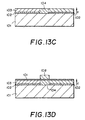
- FIG. 13A illustrates a state in which a mask 108 is formed on, for example, a NdGaO 3 substrate 101 having a lattice mismatch with respect to YBa 2 Cu 3 O x of 0.3%.
- a SrTiO 3 layer 102 having a lattice mismatch with respect to YBa 2 Cu 3 O x of 1.1% is deposited on a portion other than that covered with the mask 108.
- the mask 108 is removed.
- Fig. 13B shows an arrangement in which the mask 108 has been removed after the deposition of the SrTiO 3 layer 102.
- a YBa 2 Cu 3 O x thin film On the overall surface of the NdGaO 3 substrate 101 shown in Fig. 13B, there is deposited a YBa 2 Cu 3 O x thin film at a substrate temperature of 750°C, for example, which is shown in broken line in Fig. 3.
- a c-axis oriented YBa 2 Cu 3 O x thin film 103 is deposited on the SrTiO 3 thin film 102 and an a-axis oriented YBa 2 Cu 3 O x thin film 104 is deposited on the NdGaO 3 substrate 101.
- a NdGaO 3 ultra thin film 110 serving as a barrier layer, followed by covering a mask 108 on a portion which is designed to be a junction to obtain a structure as shown in Fig. 13D.
- an interlayer insulator 106 composed of a SrTiO 3 thin film is formed by deposition, the mask 108 is removed, and an a-axis oriented YBa 2 Cu 3 O x thin film is deposited at a substrate temperature of, for example, 750°C, which is indicated in broken line in Fig. 3 on the overall surface to obtain a structure as shown in Fig. 12.
- a c-axis oriented YBa 2 Cu 3 O x thin film 107 is deposited on the SrTiO 3 thin film 106 while an a-axis oriented YBa 2 Cu 3 O x thin film 111 is deposited on the NdGaO 3 substrate 101.
- a junction is realized in which only the junction electrodes 111 and 104 sandwiching the barrier layer 110 constituting the junction are a-axis oriented, with wiring portions other than the junction portion being c-axis oriented.
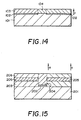
- Fig. 14 is a cross sectional view showing a superconducting vertical junction according to a seventh example.
- reference numeral 101 designates a NdGaO 3 substrate
- 102 is a SrTiO 3 thin film
- 103 is a lower electrode composed of a c-axis oriented YBa 2 Cu 3 O x thin film
- 104 is a lower electrode composed of an a-axis oriented YBa 2 Cu 3 O x thin film.
- This example differs from Examples 1 and 3 in that in this example, before the SrTiO 3 thin film 102 is deposited on the substrate 101, the substrate 101 is etched to a depth equal to the thickness of the thin film 102 to be deposited subsequently with using a mask 108 to protect a portion on which a junction is designed to be formed.
- This increases contact area in which an a-axis oriented portion constituting the junction and a c-axis oriented portion constituting a wiring contact each other, i.e., current density, and additionally achieves leveling which increases process margin.
- the substrate itself and a thin film are used as materials on whose surfaces a lower electrode is to be deposited.
- the same or similar effects can be obtained with two or more thin film materials having different lattice mismatches deposited on the substrate in the same manner as the substrate surfaces prior to deposition of upper electrode as described in Examples 5 and 6 (Fig. 9C and Fig. 13C, respectively).
- Fig. 15 is a cross sectional view showing a superconducting vertical junction according to an eighth example.
- reference numeral 201 is a StTiO 3 substrate
- 202 is a NdGaO 3 thin film
- 203 is a c-axis oriented YBa 2 Cu 3 O x thin film as a lower integrated circuit
- 204 is an a-axis oriented YBa 2 Cu 3 O x thin film serving as an interlayer wiring
- 205 is a SrTiO 3 interlayer insulator
- 206 is a c-axis oriented YBa 2 Cu 3 O x thin film serving as an upper electrode.
- the thin film in the integrated circuit is composed of a c-axis oriented thin film (direction of a smaller coherence length is perpendicular to a surface of the substrate), and the interlayer wiring 204 is composed of an a-axis oriented thin film (direction of a smaller coherence length is parallel to a surface of the substrate).
- Current which flows through the interlayer wiring transmits through the thin film 203 in the lower integrated circuit to the interlayer wiring 204 and then to the thin film 206 in the upper integrated circuit.
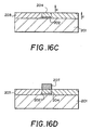
- FIG. 16A illustrates a state in which a mask 207 is formed on, for example, a SrTiO 3 substrate 201 having a lattice mismatch with respect to YBa 2 Cu 3 O x of 1.1%. Then, for example, a NdGaO 3 layer 202 having a lattice mismatch with respect to YBa 2 Cu 3 O x of 0.3% is deposited on a portion other than that covered with the mask 207.
- a c-axis oriented YBa 2 Cu 3 O x thin film 203 is deposited on the SrTiO 3 substrate 1 and an a-axis oriented YBa 2 Cu 3 O x thin film 204 is deposited on the NdGaO 3 thin film 202, as shown in Fig. 16C.
- a mask 207 is arranged on the a-axis oriented YBa 2 Cu 3 O x thin film 204 serving as an interlayer wiring to obtain a structure shown in Fig. 16D.
- a SrTiO 3 interlayer insulator 205 is deposited and the mask 207 is removed, followed by depositing a YBa 2 Cu 3 O x thin film 206 in an upper integrated circuit.
- the c-axis oriented thin film 206 grows on the SrTiO 3 interlayer insulator 205 while the a-axis oriented thin film grows on the interlayer wiring 204 as shown in Fig. 15.
- Fig. 17 is a cross sectional view showing a superconducting vertical junction according to a ninth example.
- reference numeral 201 designates a SrTiO 3 substrate
- 202 is a NdGaO 3 thin film
- 203 is a c-axis oriented YBa 2 Cu 3 O x thin film as a lower integrated circuit
- 204 is an a-axis oriented YBa 2 Cu 3 O x thin film serving as an interlayer wiring
- 205 is a SrTiO 3 interlayer insulator
- 206 is a c-axis oriented YBa 2 Cu 3 O x thin film serving as an upper electrode.
- This example differs from Example 1 in that in this example, before the NdGaO 3 thin film 202 is deposited on the SrTiO 3 substrate 201, the substrate 201 is etched to a depth equal to the thickness of the thin film 202 to be deposited subsequently with using a mask to protect a portion on which a junction is designed to be formed. This increases contact area at which an a-axis oriented portion constituting the junction and a c-axis oriented portion constituting a wiring contact each other, i.e., current density, and additionally achieves leveling which increases process margin.
- the substrate itself and a thin film are used as materials on whose surfaces a lower electrode is to be deposited.
- the same or similar effects can be obtained with two or more thin film materials having different lattice mismatches deposited on the substrate in the same manner as the substrate surfaces prior to deposition of upper electrode.
Landscapes
- Engineering & Computer Science (AREA)
- Manufacturing & Machinery (AREA)
- Chemical & Material Sciences (AREA)
- Ceramic Engineering (AREA)
- Superconductor Devices And Manufacturing Methods Thereof (AREA)
- Superconductors And Manufacturing Methods Therefor (AREA)
Claims (9)
- Supraleitendes Dünnfilm-Bauelement mit Korngrenzenübergangsbereich (5), mit:dargestellt wird, wobei Ln Yttrium oder ein Lanthanid bezeichnet und x die Beziehung 6 < x < 7 erfüllt;einem Substrat (1);einem ersten und einem zweiten monokristallinen Bereich, die auf dem Substrat angeordnet sind und Gitterfehlanpassungen bezüglich eines Supraleiters aufweisen, der durch die Formel
wobei die Gitterfehlanpassung des ersten monokristallinen Bereichs größer ist als 1% und die Gitterfehlanpassung des zweiten monokristallinen Bereichs nicht größer ist als 1%;
einem supraleitenden Dünnfilm (3, 4) aus einem Supraleiter, der durch die Formel
wobei der supraleitende Dünnfilm (3) in dem ersten monokristallinen Bereich eine senkrecht zu einer Oberfläche des supraleitenden Dünnfilms ausgerichtete c-Achse aufweist; und
der supraleitende Dünnfilm (4) in dem zweiten monokristallinen Bereich eine senkrecht zu einer Oberfläche des supraleitenden Dünnfilms ausgerichtete a-Achse aufweist. - Bauelement nach Anspruch 1, wobei das Substrat (1) aus einem aus der aus Nd:YAlO3, LaAlO3, SrLaGaO4, NdGaO3, PrGaO3, LaGaO3, SrTiO3 und MgO bestehenden Gruppe ausgewählten Material besteht.
- Bauelement nach Anspruch 1, wobei das Substrat (1) aus SrTiO3 besteht, und wobei zwischen dem Substrat (1) und dem ersten monokristallinen Bereich (4) des supraleitenden Dünnfilms (3, 4) eine PrGaO3-Schicht (2) ausgebildet ist.
- Bauelement nach Anspruch 1 oder 2, wobei das Substrat (1) aus PrGaO3 besteht, und wobei zwischen dem Substrat (1) und dem zweiten monokristallinen Bereich (3) des supraleitenden Dünnfilms (3, 4) eine SrTiO3-Schicht (2) ausgebildet ist.
- Verfahren zum Herstellen eines Dünnfilm-Bauelements mit Korngrenzen-Übergangsbereich (5), mit den Schritten:dargestellt wird, wobei Ln Yttrium oder ein Lanthanid bezeichnet und x die Beziehung 6 < x < 7 erfüllt;Bereitstellen eines Substrats (1);Ausbilden mindestens zweier monokristalliner Bereiche auf einer Oberfläche des Substrats, wobei die beiden monokristallinen Bereiche Gitterfehlanpassungen bezüglich eines Supraleiters aufweisen, der durch die Formel
wobei die Gitterfehlanpassungen mindestens eines der mindestens zwei Bereiche größer sind als 1% und die Gitterfehlanpassungen mindestens eines anderen der mindestens zwei monokristallinen Bereiche nicht größer sind als 1%;
gleichzeitiges Ausbilden eines Dünnfilms (3, 4) eines Supraleiters auf den ersten und den zweiten monokristallinen Bereichen, wobei der Supraleiter durch die Formel - Verfahren nach Anspruch 5, wobei das Substrat (1) aus einem aus der aus Nd:YAlO3, LaAlO3, SrLaGaO4, NdGaO3, PrGaO3, LaGaO3, SrTiO3 und MgO bestehenden Gruppe ausgewählten Material besteht.
- Verfahren nach Anspruch 5 oder 6, mit den Schritten:wobei die senkrecht zu einer Oberfläche des Substrats (1) ausgerichtete Orientierungsachse des Dünnfilms (3) auf dem Substrat (1) eine c-Achse und die senkrecht zu einer Oberfläche des Substrats (1) ausgerichtete Orientierungsachse des Dünnfilms (4) auf der PrGaO3-Schicht (2) eine a-Achse ist.a) Bereitstellen eines Substrats (1) aus SrTiO3;b) Abdecken eines Teils der Oberfläche des Substrats (1) durch eine Maske (6);c) Aufbringen einer PrGaO3-Schicht (2) auf einen durch die Maske (6) nicht abgedeckten Teil der Oberfläche;d) Entfernen der Maske (6); unde) Aufbringen des Dünnfilms (3, 4) des Supraleiters auf der gesamten Oberfläche des Substrats (1);
- Verfahren nach Anspruch 5 oder 6, mit den Schritten:wobei die senkrecht zu einer Oberfläche des Substrats (1) ausgerichtete Orientierungsachse des Dünnfilms (3) auf der SrTiO3-Schicht (2) eine c-Achse und die senkrecht zu einer Oberfläche des Substrats (1) ausgerichtete Orientierungsachse der Dünnfilm (4) auf dem Substrat (1) eine a-Achse ist.a) Bereitstellen eines Substrats aus PrGaO3;b) Abdecken eines Teils der Oberfläche des Substrats (1) durch eine Maske (6);c) Aufbringen einer SrTiO3-Schicht (2) auf einen durch die Maske (6) nicht abgedeckten Teil der Oberfläche des Substrats (1);d) Entfernen der Maske (6); unde) Aufbringen des Dünnfilms (3, 4) des Supraleiters auf der gesamten Oberfläche des Substrats (1);
- Verfahren nach Anspruch 5 oder 6, mit den Schritten:wobei die senkrecht zu einer Oberfläche des Substrats (1) ausgerichtete Orientierungsachse des Dünnfilms (3) auf der SrTiO3-Schicht (2) eine c-Achse und die senkrecht zu einer Oberfläche des Substrats (1) ausgerichtete Orientierungsachse des Dünnfilms (4) auf dem Substrat (1) eine a-Achse ist.a) Bereitstellen eines Substrats (1) aus PrGaO3;b) Abdecken eines Teils der Oberfläche des Substrats (1) durch eine Maske (6);c) Ätzen des Substrats (1) bis zu einer gewissen Tiefe;d) Aufbringen einer SrTiO3-Schicht (2) auf den geätzten Abschnitt des Substrats (1);e) Entfernen der Maske (6); undf) Aufbringen des Dünnfilms (3, 4) des Supraleiters auf der gesamten Oberfläche des Substrats (1);
Priority Applications (1)
| Application Number | Priority Date | Filing Date | Title |
|---|---|---|---|
| EP05005034A EP1544926A3 (de) | 1992-07-28 | 1993-07-27 | Supraleitende Dünnschicht-Vorrichtung mit Mehrlagenverdrahtung aus supraleitenden Oxiden und Herstellungsverfahren |
Applications Claiming Priority (7)
| Application Number | Priority Date | Filing Date | Title |
|---|---|---|---|
| JP22077892 | 1992-07-28 | ||
| JP4220778A JP2708671B2 (ja) | 1992-07-28 | 1992-07-28 | 超伝導薄膜粒界接合素子の製造方法。 |
| JP22379692 | 1992-08-24 | ||
| JP4223796A JP2708673B2 (ja) | 1992-08-24 | 1992-08-24 | 超伝導薄膜縦型接合素子の製造方法 |
| JP4240501A JP2708675B2 (ja) | 1992-09-09 | 1992-09-09 | 超伝導薄膜層間配線の製造方法 |
| JP24050192 | 1992-09-09 | ||
| EP93111981A EP0582889B1 (de) | 1992-07-28 | 1993-07-27 | Übergangsvorrichtung mit Gitteranpassung und Verfahren zu ihrer Herstellung |
Related Parent Applications (2)
| Application Number | Title | Priority Date | Filing Date |
|---|---|---|---|
| EP93111981A Division EP0582889B1 (de) | 1992-07-28 | 1993-07-27 | Übergangsvorrichtung mit Gitteranpassung und Verfahren zu ihrer Herstellung |
| EP93111981A Division-Into EP0582889B1 (de) | 1992-07-28 | 1993-07-27 | Übergangsvorrichtung mit Gitteranpassung und Verfahren zu ihrer Herstellung |
Related Child Applications (1)
| Application Number | Title | Priority Date | Filing Date |
|---|---|---|---|
| EP05005034A Division EP1544926A3 (de) | 1992-07-28 | 1993-07-27 | Supraleitende Dünnschicht-Vorrichtung mit Mehrlagenverdrahtung aus supraleitenden Oxiden und Herstellungsverfahren |
Publications (3)
| Publication Number | Publication Date |
|---|---|
| EP0973208A2 EP0973208A2 (de) | 2000-01-19 |
| EP0973208A3 EP0973208A3 (de) | 2000-03-08 |
| EP0973208B1 true EP0973208B1 (de) | 2005-04-27 |
Family
ID=27330476
Family Applications (3)
| Application Number | Title | Priority Date | Filing Date |
|---|---|---|---|
| EP99118017A Expired - Lifetime EP0973208B1 (de) | 1992-07-28 | 1993-07-27 | Vorrichtung mit Gitteranpassung und Verfahren zu ihrer Herstellung |
| EP93111981A Expired - Lifetime EP0582889B1 (de) | 1992-07-28 | 1993-07-27 | Übergangsvorrichtung mit Gitteranpassung und Verfahren zu ihrer Herstellung |
| EP05005034A Withdrawn EP1544926A3 (de) | 1992-07-28 | 1993-07-27 | Supraleitende Dünnschicht-Vorrichtung mit Mehrlagenverdrahtung aus supraleitenden Oxiden und Herstellungsverfahren |
Family Applications After (2)
| Application Number | Title | Priority Date | Filing Date |
|---|---|---|---|
| EP93111981A Expired - Lifetime EP0582889B1 (de) | 1992-07-28 | 1993-07-27 | Übergangsvorrichtung mit Gitteranpassung und Verfahren zu ihrer Herstellung |
| EP05005034A Withdrawn EP1544926A3 (de) | 1992-07-28 | 1993-07-27 | Supraleitende Dünnschicht-Vorrichtung mit Mehrlagenverdrahtung aus supraleitenden Oxiden und Herstellungsverfahren |
Country Status (3)
| Country | Link |
|---|---|
| US (2) | US5593950A (de) |
| EP (3) | EP0973208B1 (de) |
| DE (2) | DE69328278T2 (de) |
Families Citing this family (6)
| Publication number | Priority date | Publication date | Assignee | Title |
|---|---|---|---|---|
| JP2994183B2 (ja) * | 1993-09-21 | 1999-12-27 | 財団法人国際超電導産業技術研究センター | 超電導素子およびその作製方法 |
| KR0148596B1 (ko) * | 1994-11-28 | 1998-10-15 | 양승택 | 결정 입계 채널을 갖는 초전도 전계효과 소자와 그 제조방법 |
| KR100194621B1 (ko) * | 1995-12-21 | 1999-07-01 | 정선종 | 고온초전도 전계효과 소자 및 그 제조방법 |
| US5906965A (en) * | 1996-01-19 | 1999-05-25 | Superconductor Technologies, Inc. | Thin film superconductor-insulator-superconductor multi-layer films and method for obtaining the same |
| EP1126971A2 (de) * | 1998-09-14 | 2001-08-29 | The Regents of The University of California | Supraleiterstruktur aus gemischtensettenerd-, barium-, und kupferverbindungen |
| US6635368B1 (en) | 2001-12-20 | 2003-10-21 | The United States Of America As Represented By The Secretary Of The Navy | HTS film-based electronic device characterized by low ELF and white noise |
Family Cites Families (27)
| Publication number | Priority date | Publication date | Assignee | Title |
|---|---|---|---|---|
| US4589001A (en) * | 1980-07-09 | 1986-05-13 | Agency Of Industrial Science & Technology | Quasiparticle injection control type superconducting device |
| US4509001A (en) * | 1983-03-04 | 1985-04-02 | Matsushita Electric Industrial Co., Ltd. | Brushless linear servomotor |
| JPH0634418B2 (ja) * | 1987-09-07 | 1994-05-02 | 株式会社半導体エネルギー研究所 | 超電導素子の作製方法 |
| JPS6439084A (en) * | 1987-08-04 | 1989-02-09 | Mitsubishi Electric Corp | Josephson element |
| FR2626715B1 (fr) * | 1988-02-02 | 1990-05-18 | Thomson Csf | Dispositif en couches minces de materiau supraconducteur et procede de realisation |
| JPH01241874A (ja) * | 1988-03-23 | 1989-09-26 | Mitsubishi Electric Corp | ジョゼフソン接合素子 |
| US4962086A (en) * | 1988-06-08 | 1990-10-09 | International Business Machines Corporation | High Tc superconductor - gallate crystal structures |
| US5047385A (en) * | 1988-07-20 | 1991-09-10 | The Board Of Trustees Of The Leland Stanford Junior University | Method of forming superconducting YBa2 Cu3 O7-x thin films with controlled crystal orientation |
| EP0358879A3 (de) * | 1988-09-13 | 1991-02-27 | Hewlett-Packard Company | Verfahren zur Herstellung hochintegrierter Verbindungen |
| US5077266A (en) * | 1988-09-14 | 1991-12-31 | Hitachi, Ltd. | Method of forming weak-link josephson junction, and superconducting device employing the junction |
| JPH02253515A (ja) * | 1989-03-25 | 1990-10-12 | Showa Electric Wire & Cable Co Ltd | セラミックス超電導線路およびその形成方法 |
| CA2037795C (en) * | 1990-03-09 | 1998-10-06 | Saburo Tanaka | Process for preparing high-temperature superconducting thin films |
| JPH05894A (ja) * | 1990-06-28 | 1993-01-08 | Sumitomo Electric Ind Ltd | 複合酸化物超電導薄膜 |
| US5236896A (en) * | 1990-10-08 | 1993-08-17 | Sumitomo Electric Industries, Ltd. | Superconducting device having an extremely thin superconducting channel formed of oxide superconductor material |
| JP2703404B2 (ja) * | 1990-10-31 | 1998-01-26 | 住友電気工業株式会社 | 超電導回路とその作製方法 |
| EP0484252B1 (de) * | 1990-10-31 | 1996-03-20 | Sumitomo Electric Industries, Ltd. | Supraleitende Einrichtung aus oxydisch supraleitendem Material |
| CA2054597C (en) * | 1990-10-31 | 1997-08-19 | Hiroshi Inada | Superconducting circuit and a process for fabricating the same |
| JPH04168779A (ja) * | 1990-11-01 | 1992-06-16 | Sumitomo Electric Ind Ltd | 超電導回路とその作製方法 |
| JPH04214097A (ja) * | 1990-12-13 | 1992-08-05 | Sumitomo Electric Ind Ltd | 超電導薄膜の作製方法 |
| JPH04268774A (ja) * | 1991-02-25 | 1992-09-24 | Riken Corp | ジョセフソン接合 |
| DE69212670T2 (de) * | 1991-03-04 | 1997-03-06 | Sumitomo Electric Industries | Supraleitende oxydische Dünnschicht mit lokal unterschiedlichen Kristallorientierungen und ein Verfahren zu deren Herstellung |
| US5157466A (en) * | 1991-03-19 | 1992-10-20 | Conductus, Inc. | Grain boundary junctions in high temperature superconductor films |
| JPH04302183A (ja) * | 1991-03-29 | 1992-10-26 | Furukawa Electric Co Ltd:The | トンネル型ジョセフソン接合の形成方法 |
| DE69215993T2 (de) * | 1991-07-16 | 1997-06-19 | Sumitomo Electric Industries | Vorrichtung mit Josephson-Übergang aus supraleitendem Oxyd und Verfahren zu seiner Herstellung |
| US5430012A (en) * | 1991-12-02 | 1995-07-04 | Sumitomo Electric Industries, Ltd. | Superconducting multilayer interconnection formed of a-axis and c-axis oriented oxide superconductor materials |
| JPH05251771A (ja) * | 1991-12-02 | 1993-09-28 | Sumitomo Electric Ind Ltd | 人工粒界型ジョセフソン接合素子およびその作製方法 |
| EP0557207B1 (de) * | 1992-02-19 | 2000-05-03 | Sumitomo Electric Industries, Ltd. | Josephson-Übergangseinrichtung aus oxidischem Supraleiter und Verfahren zu ihrer Herstellung |
-
1993
- 1993-07-27 US US08/097,235 patent/US5593950A/en not_active Expired - Fee Related
- 1993-07-27 EP EP99118017A patent/EP0973208B1/de not_active Expired - Lifetime
- 1993-07-27 EP EP93111981A patent/EP0582889B1/de not_active Expired - Lifetime
- 1993-07-27 EP EP05005034A patent/EP1544926A3/de not_active Withdrawn
- 1993-07-27 DE DE69328278T patent/DE69328278T2/de not_active Expired - Fee Related
- 1993-07-27 DE DE69333799T patent/DE69333799T2/de not_active Expired - Fee Related
-
1995
- 1995-06-07 US US08/479,751 patent/US5821200A/en not_active Expired - Fee Related
Also Published As
| Publication number | Publication date |
|---|---|
| DE69328278D1 (de) | 2000-05-11 |
| EP0973208A2 (de) | 2000-01-19 |
| DE69333799T2 (de) | 2006-01-19 |
| US5593950A (en) | 1997-01-14 |
| DE69333799D1 (de) | 2005-06-02 |
| US5821200A (en) | 1998-10-13 |
| EP1544926A3 (de) | 2005-07-20 |
| EP0582889A1 (de) | 1994-02-16 |
| DE69328278T2 (de) | 2000-11-30 |
| EP0973208A3 (de) | 2000-03-08 |
| EP1544926A2 (de) | 2005-06-22 |
| EP0582889B1 (de) | 2000-04-05 |
Similar Documents
| Publication | Publication Date | Title |
|---|---|---|
| US5418216A (en) | Superconducting thin films on epitaxial magnesium oxide grown on silicon | |
| US5173474A (en) | Silicon substrate having an epitaxial superconducting layer thereon and method of making same | |
| EP0345441B1 (de) | Hochtemperatursupraleiter-Gallatkristallstruktur | |
| EP0619283A2 (de) | Substrat mit einer supraleitenden Schicht | |
| EP0576633A1 (de) | Korngrenz-uebergaenge in hochtemperatur-supraleitern | |
| JP3278638B2 (ja) | 高温超伝導ジョセフソン接合およびその製造方法 | |
| US5196395A (en) | Method for producing crystallographic boundary junctions in oxide superconducting thin films | |
| WO1991019026A1 (en) | Growth of a,b-axis oriented perovskite thin films | |
| CA2037795C (en) | Process for preparing high-temperature superconducting thin films | |
| EP0502787B1 (de) | Supraleitende oxydische Dünnschicht mit lokal unterschiedlichen Kristallorientierungen und ein Verfahren zu deren Herstellung | |
| EP0635894B1 (de) | Schichtstruktur mit isolierender Dünnschicht und Oxydsupraleiter-Dünnschicht | |
| EP0973208B1 (de) | Vorrichtung mit Gitteranpassung und Verfahren zu ihrer Herstellung | |
| EP0546904B1 (de) | Verfahren zum Herstellen eines künstlichen Josephson-Korngrenzen-Übergangselementes | |
| EP0506570B1 (de) | Verfahren zur Herstellung einer Dünnschicht aus supraleitender oxydischer Verbindung | |
| EP0341148B1 (de) | Halbleitersubstrat mit dünner Supraleiterschicht | |
| US5416062A (en) | Thin film superconductor with an interlayer on a silicon substrate | |
| EP0599699B1 (de) | Verfahren zur Herstellung einer supraleitenden Dünnschicht aus hoch-temperatur-supraleitenden-Oxid | |
| US6083884A (en) | A-axis high temperature superconducting films with preferential in-plane alignment | |
| US6194353B1 (en) | Process for preparing superconducting thin film formed of oxide superconductor material | |
| EP0466607B1 (de) | Prozess zur Abscheidung einer anderen Dünnschicht auf einen oxydischen Supraleiter | |
| AU643286B2 (en) | Process for preparing superconducting junction of oxide superconductor | |
| EP0620602A1 (de) | Verfahren zum Ablegen einer anderen Dünnschicht auf einer Oxyd-Dünnschicht mit perovskiter Kristallstruktur | |
| EP0431595B1 (de) | Dünnfilm aus supraleitendem Oxid | |
| EP0691418A1 (de) | Verfahren zum Herstellen einer hochkristallen dünnen Oxidfilms | |
| Takeuchi et al. | Heterostructure applications of in-plane oriented a-axis YBa/sub 2/Cu/sub 3/O/sub 7-x/films on LaSrGaO/sub 4 |
Legal Events
| Date | Code | Title | Description |
|---|---|---|---|
| PUAI | Public reference made under article 153(3) epc to a published international application that has entered the european phase |
Free format text: ORIGINAL CODE: 0009012 |
|
| AC | Divisional application: reference to earlier application |
Ref document number: 582889 Country of ref document: EP |
|
| AK | Designated contracting states |
Kind code of ref document: A2 Designated state(s): DE FR GB |
|
| PUAL | Search report despatched |
Free format text: ORIGINAL CODE: 0009013 |
|
| AK | Designated contracting states |
Kind code of ref document: A3 Designated state(s): DE FR GB |
|
| RIN1 | Information on inventor provided before grant (corrected) |
Inventor name: KOBAYASHI, JUNYA Inventor name: MIYAZAWA, SHINTARO Inventor name: MUKAIDA, MASASHI |
|
| 17P | Request for examination filed |
Effective date: 20000720 |
|
| AKX | Designation fees paid |
Free format text: DE FR GB |
|
| 17Q | First examination report despatched |
Effective date: 20020611 |
|
| GRAP | Despatch of communication of intention to grant a patent |
Free format text: ORIGINAL CODE: EPIDOSNIGR1 |
|
| GRAS | Grant fee paid |
Free format text: ORIGINAL CODE: EPIDOSNIGR3 |
|
| GRAA | (expected) grant |
Free format text: ORIGINAL CODE: 0009210 |
|
| AC | Divisional application: reference to earlier application |
Ref document number: 0582889 Country of ref document: EP Kind code of ref document: P |
|
| AK | Designated contracting states |
Kind code of ref document: B1 Designated state(s): DE FR GB |
|
| REG | Reference to a national code |
Ref country code: GB Ref legal event code: FG4D |
|
| REF | Corresponds to: |
Ref document number: 69333799 Country of ref document: DE Date of ref document: 20050602 Kind code of ref document: P |
|
| PLBE | No opposition filed within time limit |
Free format text: ORIGINAL CODE: 0009261 |
|
| STAA | Information on the status of an ep patent application or granted ep patent |
Free format text: STATUS: NO OPPOSITION FILED WITHIN TIME LIMIT |
|
| ET | Fr: translation filed | ||
| 26N | No opposition filed |
Effective date: 20060130 |
|
| PGFP | Annual fee paid to national office [announced via postgrant information from national office to epo] |
Ref country code: DE Payment date: 20070831 Year of fee payment: 15 |
|
| PGFP | Annual fee paid to national office [announced via postgrant information from national office to epo] |
Ref country code: GB Payment date: 20070723 Year of fee payment: 15 |
|
| PGFP | Annual fee paid to national office [announced via postgrant information from national office to epo] |
Ref country code: FR Payment date: 20070718 Year of fee payment: 15 |
|
| GBPC | Gb: european patent ceased through non-payment of renewal fee |
Effective date: 20080727 |
|
| PG25 | Lapsed in a contracting state [announced via postgrant information from national office to epo] |
Ref country code: DE Free format text: LAPSE BECAUSE OF NON-PAYMENT OF DUE FEES Effective date: 20090203 |
|
| REG | Reference to a national code |
Ref country code: FR Ref legal event code: ST Effective date: 20090331 |
|
| PG25 | Lapsed in a contracting state [announced via postgrant information from national office to epo] |
Ref country code: GB Free format text: LAPSE BECAUSE OF NON-PAYMENT OF DUE FEES Effective date: 20080727 |
|
| PG25 | Lapsed in a contracting state [announced via postgrant information from national office to epo] |
Ref country code: FR Free format text: LAPSE BECAUSE OF NON-PAYMENT OF DUE FEES Effective date: 20080731 |