EP0448069B1 - Circuit à diversité et circuit d'estimation de phase de trame (ou de temporisation d'échantillonnage) utilisant le circuit à diversité - Google Patents
Circuit à diversité et circuit d'estimation de phase de trame (ou de temporisation d'échantillonnage) utilisant le circuit à diversité Download PDFInfo
- Publication number
- EP0448069B1 EP0448069B1 EP91104319A EP91104319A EP0448069B1 EP 0448069 B1 EP0448069 B1 EP 0448069B1 EP 91104319 A EP91104319 A EP 91104319A EP 91104319 A EP91104319 A EP 91104319A EP 0448069 B1 EP0448069 B1 EP 0448069B1
- Authority
- EP
- European Patent Office
- Prior art keywords
- power
- circuit
- computing
- received signal
- transmission channel
- Prior art date
- Legal status (The legal status is an assumption and is not a legal conclusion. Google has not performed a legal analysis and makes no representation as to the accuracy of the status listed.)
- Expired - Lifetime
Links
Images


Classifications
-
- H—ELECTRICITY
- H04—ELECTRIC COMMUNICATION TECHNIQUE
- H04L—TRANSMISSION OF DIGITAL INFORMATION, e.g. TELEGRAPHIC COMMUNICATION
- H04L1/00—Arrangements for detecting or preventing errors in the information received
- H04L1/02—Arrangements for detecting or preventing errors in the information received by diversity reception
- H04L1/06—Arrangements for detecting or preventing errors in the information received by diversity reception using space diversity
-
- H—ELECTRICITY
- H04—ELECTRIC COMMUNICATION TECHNIQUE
- H04L—TRANSMISSION OF DIGITAL INFORMATION, e.g. TELEGRAPHIC COMMUNICATION
- H04L25/00—Baseband systems
- H04L25/02—Details ; arrangements for supplying electrical power along data transmission lines
- H04L25/0202—Channel estimation
- H04L25/0204—Channel estimation of multiple channels
-
- H—ELECTRICITY
- H04—ELECTRIC COMMUNICATION TECHNIQUE
- H04L—TRANSMISSION OF DIGITAL INFORMATION, e.g. TELEGRAPHIC COMMUNICATION
- H04L25/00—Baseband systems
- H04L25/02—Details ; arrangements for supplying electrical power along data transmission lines
- H04L25/0202—Channel estimation
- H04L25/0212—Channel estimation of impulse response
Definitions
- the present invention relates to a diversity circuit and a frame phase (or sampling timing) estimation circuit which uses the diversity circuit, in digital radio communication.
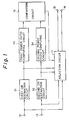
- Fig. 1 is a block diagram illustrating a diversity circuit according to a prior art such as the one disclosed in the literature titled "A New Post-detection Selection Diversity with MLSE ( M aximum L ikelihood S equence E stimation) Equalization” (Autumnal National Session of the Institute of Electronics, Information and Communication Engineers, 1989, B-502, pp. 2 - 172).
- MLSE M aximum L ikelihood S equence E stimation
- numeral 10 designates a comparison circuit adapted to compare a power ratio
- numeral 11 a selection circuit adapted to output the optimum received signal and an estimated value of the channel characteristics such as an estimated channel impulse response (CIR) respectively to output terminal 15 for selected received signal and output terminal 16 for the selected estimated CIR value
- numerals 31, 32 respectively a first CIR estimation circuit and a second CIR estimation circuit adapted to estimate CIR on the basis of the received signals input to the input terminals 12, 13 and a transmission pattern which is known
- numerals 33, 34 respectively a first power ratio computing circuit and a second power ratio computing circuit adapted to obtain the power ratio of the estimated CIR.
- the signals which have been received by antennas (not shown) installed at different locations spaced from each other are detected by respective detection circuits (not shown) and then input to the input terminals 12, 13 as the received signals.
- the first CIR estimation circuit 31 and the second CIR estimation circuit 32 receive the respective received signals and compute estimated CIR values for the respective input systems and output the computed values (Step ST21).
- the first power ratio computing circuit 33 and the second power ratio computing circuit 34 are adapted to receive the respective estimated CIR values and compute the ratio of the power component to be used in the maximum likelihood sequence estimation (MLSE) section at the later stage (not shown) (i.e., the power within the processing range) relative to the power out of the range of MLSE equalization (i.e., the power out of the processing range) (Step ST22).
- the comparison circuit 10 is adapted to receive the respective power ratios and output a selected signal designating the received signal which corresponds to the largest power ratio or the received signal which is supposed to have the largest equivalent S/N ratio.
- the selection circuit 11 is then adapted to output the received signal and the estimated CIR value corresponding to the selection signal.
- Fig. 3 is an explanatory diagram showing an example of the relationship between the estimated CIR and the actual CIR.
- the solid line designates the estimated CIR while the dotted line designates the actual CIR.
- the power ratios of the CIR power within the processing range relative to the CIR power out of the processing range are computed and the power ratio designating that the power is most concentrated in the processing range is selected.
- the estimated CIR values for the received signals input to the two input terminals 12, 13 have exactly the same values but only the noise power respectively corresponding to these received signals are different from one another. In this case, the received signal corresponding to the smaller noise power should be selected.
- the probability of such a selection being made is 0.5.
- Another consideration is also made in respect of the case in which the estimated CIR values for the received signals are exactly the same but the relationship between the estimated CIR values and the actual CIR values are respectively as illustrated by symbols (A) and (B) of Fig. 3.
- the received signal corresponding to the smaller error in CIR estimation shown by symbol (A) of Fig. 3 should be selected, but the probalility of such a selection being made 0,5.
- the present invention is directed to eliminate the problem as mentioned above and an object of the present invention is to provide a diversity circuit capable of selecting a proper received signal even when the noise power and CIR estimation errors are considerable and a frame phase (or sampling timing) estimation circuit using the diversity circuit.
- the error computing circuit computes the estimated CIR power from the estimated CIR value, for example by calculating the squared value of the estimated CIR value, estimates a received signal based on the estimated CIR value and the known transmission pattern, computes the error power between the power of the actual received signal and the power of the estimated received signal, and computes the power ratio of the estimated CIR power to the error power to output this power ratio which has taken the noise power and CIR estimation error into consideration for each received signal.
- a frame phase (or sampling timing) estimation circuit using the diversity circuit according to the present invention comprises, at the front stage of the diversity circuit, a delay circuit for providing a received signal with a plurality of different delays to output a plurality of different delayed received signals to transmission channel characteristic estimation circuits of said diversity circuit, whereby the respective delayed received signals are treated as respective received signals in said diversity circuit.
- FIG. 4 designate respectively a first arithmetic circuit, a second arithmetic circuit and a third arithmetic circuit which are adapted to output the estimated CIR value, and the power ratio of the estimated CIR power relative to the error power.
- the rest of the elements in Fig. 4 are the same as those designated by the same numerals as those in Fig. 1.
- Fig. 5 is a block diagram illustrating the constitution of the first arithmetic circuit 7.
- Fig. 4 designate respectively a first arithmetic circuit, a second arithmetic circuit and a third arithmetic circuit which are adapted to output the estimated CIR value, and the power ratio of the estimated CIR power relative to the error power.
- Fig. 5 is a block diagram illustrating the constitution of the first arithmetic circuit 7.
- Fig. 5 is a block diagram illustrating the constitution of the first arithmetic circuit 7.
- numeral 1 designates a transmission channel characteristic estimation circuit adapted to output such estimated transmission channel characteristic as estimated CIR values to an output terminal 5 and an error computing circuit 2 which outputs the power ratio to an output terminal 4.
- Fig. 6 is a flow chart illustrating an operation of the respective arithmetic circuits 7, 8, 9.
- the CIR estimation circuit 1 of the first arithmetic circuit 7 estimates the CIR on the basis of the received signal input to the input terminal 12 in the conventional manner and outputs the estimated CIR value (Step ST11).
- the error computing circuit 2 calculates the squared value of the estimated CIR value as the estimated CIR power (Step ST12).
- Received signals are estimated on the basis of the actual received signals and the known transmission pattern such as preambles of frames (Step ST13).
- the squared value of the error between the actual received signal and the estimated received signal is computed as error power (Step ST14).
- the power ratio of the estimated CIR power relative to the error power is computed (Step ST15).
- the second arithmetic circuit 8 and the third arithmetic circuit 9 also receive the received signals at the respective input terminals 13, 14 and output the power ratio and estimated CIR value respectively by a similar operation to that of the first arithmetic circuit 7.
- the comparison circuit 10 is adapted to compare the respective power ratios and output to the selection circuit 11 the selection signal specifying the received signal corresponding to the largest power ratio.
- the selection circuit 11 selects the received signal specified by said selection signal, and the estimated CIR value acquired from this received signal and outputs them to the output terminals 15, 16.
- Fig. 7 illustrates an example of the relationship between the estimated CIR and the actual CIR.
- CIR within the processing range alone becomes the estimated CIR and CIR out of the processing range contributes to the error power.
- Consideration is here made in respect of the case in which estimated CIR values for the received signals input to the two input terminals 12, 13 are exactly equal but the noise powers related to these received signals are different each other. In this case, the received signal corresponding to the smaller error power should be selected, thus the received signal having a small noise power is selected.
- Fig. 8 is a block diagram showing a frame phase (sampling timing) estimation circuit according to an embodiment of the present invention.
- numeral 20 designates an input terminal for the received signals
- numeral 21 designates a delay circuit such as a shift register adapted to provide received signals with sequential delays and the other elements are the same as those shown in Fig. 4.
- the delayed received signals output from the respective taps of the delay circuit 21 are input to the input terminals 12, 13, 14. It is to be noted here that the delayed received signal input to the input terminal 13 is delayed by ⁇ T from the received signal input to the input terminal 14 and the delayed received signal input to the input terminal 12 is delayed by 2 ⁇ T from the received signal input to the input terminal 14.
- the delay ⁇ T the inverse of the symbol rate of the signal to be transmitted is established.
- the respective arithmetic circuits 7, 8, 9, and the selection circuit 11, which have respectively input the respective delayed received signals, and the comparison circuit 10 are caused to operate in a manner similar to that of the apparatus shown in Fig. 4 and output the received signal having an optimum delay and the estimated CIR value to the output terminals 15, 16.
- the circuit provided at the later stage could demodulate the selected delayed received signal, then receiving can be carried out from the top of the frame.
- the respective embodiments as described above had three input terminals 12, 13, 14, the number of said input terminals can be increased. If the input terminals are increased, then the effect of diversity can be enhanced and the estimation range of the top phase of a frame can be further extended.
- the diversity circuit and the frame phase (sampling timing) estimation circuit using the diversity circuit are adapted to estimate the input signals from estimated CIR values, and select the optimum input signal by using the power ratio of the estimated CIR power relative to the error power between the estimated input signals and the actual input signals, even if the noise power and CIR estimation error are considerable, proper input signal may be selected.
Landscapes
- Engineering & Computer Science (AREA)
- Computer Networks & Wireless Communication (AREA)
- Signal Processing (AREA)
- Power Engineering (AREA)
- Radio Transmission System (AREA)
- Synchronisation In Digital Transmission Systems (AREA)
Claims (6)
- Circuit de diversité destiné à recevoir une pluralité de signaux reçus qui ont été propagés à travers une pluralité de trajets de signaux différents et destiné à sélectionner un signal reçu optimal, ledit circuit de diversité comprenantdes moyens d'estimation (1) des caractéristiques de la voie de transmission afin de calculer la valeur estimée des caractéristiques de la voie de transmission représentant les caractéristiques estimées de la voie de transmission du trajet de signal à partir du signal reçu, pour chacun de ladite pluralité de signaux reçus;des moyens (2) pour calculer la puissance des caractéristiques estimées de la voie de transmission à partir de ladite valeur estimée pour chaque signal reçu;des moyens (2) pour estimer un signal reçu à partir de ladite valeur estimée et du modèle de transmission qui est connu d'avance, pour chaque signal reçu;des moyens (2) pour calculer les rapports de puissance etdes moyens (10, 11) pour comparer les rapports de puissance respectifs afin de sélectionner et de délivrer les signaux reçus correspondant au rapport de puissance maximal,caractérisé par:des moyens (2) pour calculer la puissance d'erreur entre la puissance du signal estimé reçu et la puissance dudit signal reçu correspondant pour chaque signal reçu etlesdits moyens (2) pour calculer les rapports de puissance calculant le rapport de puissance de ladite puissance des caractéristiques estimées de la voie de transmission à ladite puissance d'erreur correspondante pour chaque signal reçu.
- Circuit de diversité selon la revendication 1, caractérisé par la présence d'une pluralité de bornes d'entrée (12 à 14) destinées à recevoir des signaux reçus respectifs, de circuits d'estimation de la caractéristique de la voie de transmission (1) conçus pour correspondre à ladite pluralité de bornes d'entrée (12 à 14), de circuits de calcul de l'erreur (2) conçus pour correspondre auxdits circuits d'estimation de la caractéristique respective de la voie de transmission et formant lesdits moyens destinés à calculer la puissance des caractéristiques estimées de la voie de transmission, lesdits moyens destinés à estimer un signal reçu, lesdits moyens destinés à calculer la puissance d'erreur et lesdits moyens destinés à calculer les rapports de puissance,
lesdits moyens destinés à comparer les rapports de puissance respectifs et destinés à sélectionner et à délivrer le signal reçu comprenant, un circuit de comparaison pour comparer les rapports de puissance respectifs délivrés respectivement par lesdits circuits de calcul d'erreur, pour délivrer le signal de sélection désignant le trajet de signal qui correspond au rapport de puissance maximal, et un circuit de sélection (11) pour délivrer le signal reçu et la valeur estimée de la voie de transmission, qui correspondent audit trajet de signal désigné par ledit signal de sélection, parmi lesdits signaux reçus estimés et lesdites valeurs respectives estimées des caractéristiques de transmission. - Circuit de diversité selon la revendication 1, caractérisé en ce que lesdits moyens (10, 11) destinés à sélectionner et à délivrer le signal reçu qui correspond au rapport de puissance maximal sélectionnent et délivrent en outre la valeur estimée de la voie de transmission correspondant au rapport de puissance maximal.
- Circuit de diversité selon l'une quelconque des revendications 1 à 3, caractérisé en ce que lesdites caractéristiques de la voie de transmission comprennent une réponse impulsionnelle de la voie.
- Circuit de diversité selon la revendication 1, caractérisé en ce que lesdits moyens d'estimation (1) des caractéristiques de la voie de transmission, lesdits moyens (2) destinés à calculer la puissance des caractéristiques estimées de la voie de transmission, lesdits moyens (2) destinés à estimer un signal reçu, lesdits moyens (2) destinés à calculer la puissance d'erreur, et lesdits moyens (2) destinés à calculer le rapport de puissance sont adaptés aux signaux reçus respectifs.
- Circuit d'estimation de la phase de trame (ou de la cadence d'échantillonnage) utilisant un circuit de diversité selon l'une quelconque des revendications 1 à 5, comprenant un circuit à retard (21) destiné à produire ladite pluralité de signaux reçus présentant différents retards.
Applications Claiming Priority (2)
| Application Number | Priority Date | Filing Date | Title |
|---|---|---|---|
| JP70557/90 | 1990-03-20 | ||
| JP7055790 | 1990-03-20 |
Publications (3)
| Publication Number | Publication Date |
|---|---|
| EP0448069A2 EP0448069A2 (fr) | 1991-09-25 |
| EP0448069A3 EP0448069A3 (en) | 1993-05-05 |
| EP0448069B1 true EP0448069B1 (fr) | 1996-08-28 |
Family
ID=13434950
Family Applications (1)
| Application Number | Title | Priority Date | Filing Date |
|---|---|---|---|
| EP91104319A Expired - Lifetime EP0448069B1 (fr) | 1990-03-20 | 1991-03-20 | Circuit à diversité et circuit d'estimation de phase de trame (ou de temporisation d'échantillonnage) utilisant le circuit à diversité |
Country Status (5)
| Country | Link |
|---|---|
| US (1) | US5164964A (fr) |
| EP (1) | EP0448069B1 (fr) |
| AU (1) | AU634035B2 (fr) |
| CA (1) | CA2037824C (fr) |
| DE (1) | DE69121611T2 (fr) |
Families Citing this family (20)
| Publication number | Priority date | Publication date | Assignee | Title |
|---|---|---|---|---|
| JP2683665B2 (ja) * | 1991-11-27 | 1997-12-03 | 日本電気株式会社 | 最尤系列推定装置 |
| JPH07123257B2 (ja) * | 1992-12-25 | 1995-12-25 | 日本電気株式会社 | ディジタルデータ復調装置 |
| US5349606A (en) * | 1992-12-31 | 1994-09-20 | Gte Government Systems Corporation | Apparatus for multipath DSSS communications |
| US5465412A (en) * | 1993-05-19 | 1995-11-07 | Motorola, Inc. | Apparatus and method for determining a point in time for detecting a sampled signal in a receiver |
| US5351274A (en) * | 1993-08-20 | 1994-09-27 | General Electric Company | Post detection selection combining diversity receivers for mobile and indoor radio channels |
| US5440590A (en) * | 1993-11-01 | 1995-08-08 | Motorola, Inc. | Method and apparatus for producing a usable signal from received diverse modulated signals |
| US5687197A (en) * | 1995-07-07 | 1997-11-11 | Motorola, Inc. | Method and apparatus for detecting data symbols in a diversity communication system |
| JP3674111B2 (ja) * | 1995-10-25 | 2005-07-20 | 三菱電機株式会社 | データ伝送装置 |
| US5838739A (en) * | 1996-03-29 | 1998-11-17 | Ericsson Inc. | Channel estimator circuitry, and associated method, for a digital communication system |
| FI101659B1 (fi) | 1996-07-12 | 1998-07-31 | Nokia Mobile Phones Ltd | Viiveen estimointimenetelmä ja vastaanotin |
| US5909465A (en) * | 1996-12-05 | 1999-06-01 | Ericsson Inc. | Method and apparatus for bidirectional demodulation of digitally modulated signals |
| US6335954B1 (en) | 1996-12-27 | 2002-01-01 | Ericsson Inc. | Method and apparatus for joint synchronization of multiple receive channels |
| JP3300252B2 (ja) * | 1997-04-02 | 2002-07-08 | 松下電器産業株式会社 | 適応送信ダイバーシチ装置及び適応送信ダイバーシチ方法 |
| JP3986209B2 (ja) | 1998-06-18 | 2007-10-03 | 三菱電機株式会社 | ビットタイミング同期装置およびその方法 |
| EP1073214B1 (fr) | 1999-02-16 | 2008-12-17 | Mitsubishi Denki Kabushiki Kaisha | Systeme de communication radio, emetteur et recepteur |
| FR2791841B1 (fr) * | 1999-04-02 | 2001-05-11 | Commissariat Energie Atomique | Module recepteur et recepteur compose de plusieurs modules montes en cascade |
| EP1115216A4 (fr) | 1999-07-07 | 2006-07-05 | Mitsubishi Electric Corp | Recepteur et procede d'egalisation adaptative |
| GB2353181A (en) * | 1999-08-10 | 2001-02-14 | Fujitsu Ltd | Channel estimation in mobile communications networks |
| US6717985B1 (en) * | 2000-03-08 | 2004-04-06 | Telefonaktiebolaget Lm Ericsson (Publ) | Technique for efficiently equalizing a transmission channel in a data transmission system |
| JP3844951B2 (ja) * | 2000-09-21 | 2006-11-15 | 三菱電機株式会社 | 受信機および適応等化処理方法 |
Family Cites Families (9)
| Publication number | Priority date | Publication date | Assignee | Title |
|---|---|---|---|---|
| US4935940A (en) * | 1967-05-24 | 1990-06-19 | The United States Of America As Represented By The Secretary Of The Army | Interference-proof reception of radio signals using frequency hopping techniques |
| US4217586A (en) * | 1977-05-16 | 1980-08-12 | General Electric Company | Channel estimating reference signal processor for communication system adaptive antennas |
| US4519096A (en) * | 1979-10-15 | 1985-05-21 | Motorola, Inc. | Large dynamic range multiplier for a maximal-ratio diversity combiner |
| US4715048A (en) * | 1986-05-02 | 1987-12-22 | Canadian Patents And Development Limited | Frequency offset diversity receiving system |
| US4733402A (en) * | 1987-04-23 | 1988-03-22 | Signatron, Inc. | Adaptive filter equalizer systems |
| US4972423A (en) * | 1988-12-30 | 1990-11-20 | Alfano Robert R | Method and apparatus for generating ultrashort light pulses |
| DE69024525T2 (de) * | 1989-05-02 | 1996-05-15 | Nippon Electric Co | TDMA-Raumdiversity-Empfänger |
| CA2021232C (fr) * | 1989-07-17 | 1993-09-21 | Hiroyasu Muto | Systeme de reception en diversite pour les radiocommunications numeriques a dispositif de selection de branche par evaluation du trajet de propagation |
| US5031193A (en) * | 1989-11-13 | 1991-07-09 | Motorola, Inc. | Method and apparatus for diversity reception of time-dispersed signals |
-
1991
- 1991-03-08 CA CA002037824A patent/CA2037824C/fr not_active Expired - Fee Related
- 1991-03-11 US US07/667,457 patent/US5164964A/en not_active Expired - Lifetime
- 1991-03-13 AU AU72889/91A patent/AU634035B2/en not_active Ceased
- 1991-03-20 EP EP91104319A patent/EP0448069B1/fr not_active Expired - Lifetime
- 1991-03-20 DE DE69121611T patent/DE69121611T2/de not_active Expired - Fee Related
Also Published As
| Publication number | Publication date |
|---|---|
| CA2037824C (fr) | 1999-11-09 |
| EP0448069A2 (fr) | 1991-09-25 |
| EP0448069A3 (en) | 1993-05-05 |
| DE69121611D1 (de) | 1996-10-02 |
| AU7288991A (en) | 1991-09-26 |
| AU634035B2 (en) | 1993-02-11 |
| DE69121611T2 (de) | 1997-03-06 |
| CA2037824A1 (fr) | 1991-09-21 |
| US5164964A (en) | 1992-11-17 |
Similar Documents
| Publication | Publication Date | Title |
|---|---|---|
| EP0448069B1 (fr) | Circuit à diversité et circuit d'estimation de phase de trame (ou de temporisation d'échantillonnage) utilisant le circuit à diversité | |
| JP2715662B2 (ja) | 時分割信号のダイバーシチ受信のための方法および装置 | |
| EP0604208B1 (fr) | Equilibreur adaptatif | |
| JP2556179B2 (ja) | ダイバーシティ受信方式 | |
| EP0449327B1 (fr) | Récepteur à diversité d'espace et à immunité contre le bruit | |
| CA2036423C (fr) | Methode pour reduire l'effet du a l'evanouissement dans un recepteur viterbi a antennes multiples | |
| US4271525A (en) | Adaptive diversity receiver for digital communications | |
| US5444739A (en) | Equalizer for data receiver apparatus | |
| EP0500326B1 (fr) | Equipement mobile digital de poste terminal de communication et méthode de réception pour celui-ci | |
| CA2076061A1 (fr) | Methode de fabrication d'estimateur de canaux radio a intensite de signal variable avec le temps | |
| JP2000049662A (ja) | Cdma受信装置における復調回路 | |
| JP2000082978A (ja) | 復調器 | |
| US5673288A (en) | System and method for adaptive maximum likelihood sequence estimation | |
| US5140617A (en) | Frame phase estimation method and circuit | |
| US5299231A (en) | Method and device for estimating the carrier frequency of a modulated data signal | |
| US6970524B1 (en) | Methods and systems for symbol timing recovery | |
| US6956916B1 (en) | Delayed decision feedback sequence estimation diversity receiver | |
| JPH11127208A (ja) | パイロットシンボル及び仮判定データシンボルを用いた同期検波方法及び移動体通信用受信装置及び干渉除去装置 | |
| US7269437B2 (en) | Transmission power control circuit using W-CDMA method | |
| JPH098715A (ja) | 適応等化方法及び適応等化器 | |
| JP3336991B2 (ja) | スペクトル拡散通信用受信装置 | |
| JPH118575A (ja) | 最尤系列推定受信装置 | |
| US6292510B1 (en) | Automatic equalization method and automatic equalizer | |
| KR20000048164A (ko) | 기지국 장치 및 송신 브랜치 선택 방법 | |
| JP2600970B2 (ja) | ダイバーシティ受信装置 |
Legal Events
| Date | Code | Title | Description |
|---|---|---|---|
| PUAI | Public reference made under article 153(3) epc to a published international application that has entered the european phase |
Free format text: ORIGINAL CODE: 0009012 |
|
| AK | Designated contracting states |
Kind code of ref document: A2 Designated state(s): DE FR GB SE |
|
| PUAL | Search report despatched |
Free format text: ORIGINAL CODE: 0009013 |
|
| AK | Designated contracting states |
Kind code of ref document: A3 Designated state(s): DE FR GB SE |
|
| 17P | Request for examination filed |
Effective date: 19930618 |
|
| 17Q | First examination report despatched |
Effective date: 19950505 |
|
| GRAH | Despatch of communication of intention to grant a patent |
Free format text: ORIGINAL CODE: EPIDOS IGRA |
|
| GRAH | Despatch of communication of intention to grant a patent |
Free format text: ORIGINAL CODE: EPIDOS IGRA |
|
| GRAA | (expected) grant |
Free format text: ORIGINAL CODE: 0009210 |
|
| AK | Designated contracting states |
Kind code of ref document: B1 Designated state(s): DE FR GB SE |
|
| REF | Corresponds to: |
Ref document number: 69121611 Country of ref document: DE Date of ref document: 19961002 |
|
| ET | Fr: translation filed | ||
| PLBE | No opposition filed within time limit |
Free format text: ORIGINAL CODE: 0009261 |
|
| STAA | Information on the status of an ep patent application or granted ep patent |
Free format text: STATUS: NO OPPOSITION FILED WITHIN TIME LIMIT |
|
| 26N | No opposition filed | ||
| REG | Reference to a national code |
Ref country code: GB Ref legal event code: 746 Effective date: 20000126 |
|
| REG | Reference to a national code |
Ref country code: FR Ref legal event code: D6 |
|
| REG | Reference to a national code |
Ref country code: GB Ref legal event code: IF02 |
|
| PGFP | Annual fee paid to national office [announced via postgrant information from national office to epo] |
Ref country code: SE Payment date: 20080306 Year of fee payment: 18 Ref country code: GB Payment date: 20080326 Year of fee payment: 18 |
|
| PGFP | Annual fee paid to national office [announced via postgrant information from national office to epo] |
Ref country code: FR Payment date: 20080311 Year of fee payment: 18 Ref country code: DE Payment date: 20080313 Year of fee payment: 18 |
|
| EUG | Se: european patent has lapsed | ||
| GBPC | Gb: european patent ceased through non-payment of renewal fee |
Effective date: 20090320 |
|
| REG | Reference to a national code |
Ref country code: FR Ref legal event code: ST Effective date: 20091130 |
|
| PG25 | Lapsed in a contracting state [announced via postgrant information from national office to epo] |
Ref country code: DE Free format text: LAPSE BECAUSE OF NON-PAYMENT OF DUE FEES Effective date: 20091001 |
|
| PG25 | Lapsed in a contracting state [announced via postgrant information from national office to epo] |
Ref country code: FR Free format text: LAPSE BECAUSE OF NON-PAYMENT OF DUE FEES Effective date: 20091123 Ref country code: GB Free format text: LAPSE BECAUSE OF NON-PAYMENT OF DUE FEES Effective date: 20090320 |
|
| PG25 | Lapsed in a contracting state [announced via postgrant information from national office to epo] |
Ref country code: SE Free format text: LAPSE BECAUSE OF NON-PAYMENT OF DUE FEES Effective date: 20090321 |