EP0448074A2 - Synchronization circuit for ATM cells - Google Patents
Synchronization circuit for ATM cells Download PDFInfo
- Publication number
- EP0448074A2 EP0448074A2 EP91104331A EP91104331A EP0448074A2 EP 0448074 A2 EP0448074 A2 EP 0448074A2 EP 91104331 A EP91104331 A EP 91104331A EP 91104331 A EP91104331 A EP 91104331A EP 0448074 A2 EP0448074 A2 EP 0448074A2
- Authority
- EP
- European Patent Office
- Prior art keywords
- crc
- unit
- crc arithmetic
- bit
- output
- Prior art date
- Legal status (The legal status is an assumption and is not a legal conclusion. Google has not performed a legal analysis and makes no representation as to the accuracy of the status listed.)
- Granted
Links
Images


Classifications
-
- H—ELECTRICITY
- H04—ELECTRIC COMMUNICATION TECHNIQUE
- H04Q—SELECTING
- H04Q11/00—Selecting arrangements for multiplex systems
- H04Q11/04—Selecting arrangements for multiplex systems for time-division multiplexing
- H04Q11/0428—Integrated services digital network, i.e. systems for transmission of different types of digitised signals, e.g. speech, data, telecentral, television signals
- H04Q11/0478—Provisions for broadband connections
-
- H—ELECTRICITY
- H04—ELECTRIC COMMUNICATION TECHNIQUE
- H04L—TRANSMISSION OF DIGITAL INFORMATION, e.g. TELEGRAPHIC COMMUNICATION
- H04L7/00—Arrangements for synchronising receiver with transmitter
- H04L7/04—Speed or phase control by synchronisation signals
- H04L7/048—Speed or phase control by synchronisation signals using the properties of error detecting or error correcting codes, e.g. parity as synchronisation signal
-
- H—ELECTRICITY
- H04—ELECTRIC COMMUNICATION TECHNIQUE
- H04L—TRANSMISSION OF DIGITAL INFORMATION, e.g. TELEGRAPHIC COMMUNICATION
- H04L12/00—Data switching networks
- H04L12/54—Store-and-forward switching systems
- H04L12/56—Packet switching systems
- H04L12/5601—Transfer mode dependent, e.g. ATM
- H04L2012/5672—Multiplexing, e.g. coding, scrambling
- H04L2012/5673—Coding or scrambling
-
- H—ELECTRICITY
- H04—ELECTRIC COMMUNICATION TECHNIQUE
- H04L—TRANSMISSION OF DIGITAL INFORMATION, e.g. TELEGRAPHIC COMMUNICATION
- H04L12/00—Data switching networks
- H04L12/54—Store-and-forward switching systems
- H04L12/56—Packet switching systems
- H04L12/5601—Transfer mode dependent, e.g. ATM
- H04L2012/5672—Multiplexing, e.g. coding, scrambling
- H04L2012/5674—Synchronisation, timing recovery or alignment
Definitions
- the present invention relates to a synchronization circuit, in particularly a synchronization circuit in an asynchronous transfer mode (ATM) communication system for synchronization of ATM cells connected on the lines in the system, that is, cell synchronization.
- ATM asynchronous transfer mode
- the CCITT is proposing ATM communications suitable for broad band ISDN's etc., that is, data transfer by an asynchronous transfer mode, and is pressing forward with standardization of such systems.
- One proposal is for use of a full ATM for a layer 1.
- CRC cyclic redundancy check
- ATM cells are comprised of the above header and a payload for transmitting the inherent information.
- the header also includes a field known as a header error control (HEC).
- HEC header error control
- the result of the CRC arithmetic operation are written into this HEC.
- the present invention relates to a synchronization circuit which writes, at the transmission side of the ATM cell, the result of the CRC arithmetic operation on the header in the HEC as a cell synchronization establishment signal and detects, at the reception side of the ATM cell, the coincidence of the results of the CRC arithmetic operation on the header of the ATM cell received and the result of the CRC arithmetic operation written at the transmission side in the HEC of the ATM cell received so as to detect if cell synchronization has been achieved and outputs a synchronization detection signal.
- conventional CRC arithmetic units basically are constructed to receive input bit trains having definite time series, perform CRC arithmetic operations on the trains, and obtain a CRC arithmetic operation result.
- a synchronization circuit of the full ATM transmission system does not cover such input bit trains having definite time series, but cover input bit trains having indefinite time series (ATM cell groups), so it is necessary to shift the input bit trains one bit at a time to continuously obtain CRC arithmetic operation results C outo
- the present invention in view of the above-mentioned problems, has as its object the provision of a synchronization circuit provided with a CRC arithmetic unit which can obtain continuous CRC arithmetic operation results from input bit trains comprised of indefinite time series without increasing the processing delay and without increasing the size of the apparatus even in the case of ultrahigh speed data of several 100 Mb/s or more.
- the synchronization circuit of the present invention includes a shift register unit, a continuous CRC arithmetic unit, and a synchronization control unit.
- the shift register unit receives and holds in a bit serial form the input bit trains comprising the ATM cells provided for the data transfer.
- the continuous CRC arithmetic unit performs the CRC arithmetic operation in accordance with a simplified CRC arithmetic operation process comprising a conventional CRC arithmetic operation process modified in advance to reduce the amount of operations.
- the synchronization control unit receives as input the CRC arithmetic operation result from the continuous CRC arithmetic unit.
- the ATM cells On the transmission side of the ATM cells, it inserts the CRC arithmetic operation result in the ATM cells as the synchronization establishment signal and sends the same, while on the reception side of the ATM cells, it outputs a synchronization detection signal when the CRC arithmetic operation result transmitted from the transmission side and the CRC arithmetic operation result obtained by the operations of the continuous CRC arithmetic unit on the reception side coincide.
- Figure 1 is a view of a first example of a conventional CRC arithmetic unit.
- the first conventional example (Fig. 1) is of a type which reads out the CRC arithmetic operation results by a table and includes a ROM 11 storing the table, that is, a ROM table.
- the input bit trains B in are considered as addresses of the ROM 11 and the data read out at this time is the CRC arithmetic operation result sought.
- Figure 2 is a view of a second example of a conventional CRC arithmetic unit.
- the second conventional example (Fig. 2) is of a so-called shift register type and includes serially connected shift registers 12 and exclusive OR gates (EX-OR) 13 inserted between the shift registers.
- the exclusive OR gates 13 have connectors 14 connected to them.
- the connectors 14 connect or do not connect (truth value set to "0") the CRC arithmetic operation results C out ' in accordance with the coefficients of each order of the general polynomials used in the CRC arithmetic operation ("1" or "0"). Subtraction by the EX-OR 13 is not performed when the coefficient is "0".
- the values of all shift registers 12 are cleared to "0", then bit trains are successively input from the left side of the figure.
- the values of all shift registers 12 ( ⁇ 0, ⁇ 1... xn . 1 ) when the final bit is input to the shift register 12 ( xo ) at the left side show the CRC arithmetic operation result sought. Therefore, the values of ⁇ o to ⁇ n-1 are read out at that point of time and the arranged value C out is the value sought.
- Figure 3 is a view of an example of an improvement of the first example of the conventional CRC arithmetic unit.
- the improved version of the first example of the conventional CRC arithmetic unit is a type which reads out the CRC arithmetic operation result and is comprised of a combination of a plurality of ROM tables and a plurality of EX-OR logic gates, with a plurality of ROM's 11 and a plurality of exclusive OR gates (EX-OR) 13 being connected in parallel as illustrated.
- EX-OR exclusive OR gates
- the contents of these ROM's 11 differ, however, so the ROM's are referred to as the ROM 1, ROM 2•••.
- the ROM 1 contains arithmetic operation results of "XXX•••X 000•••0"(XXX•••X being the «1 bit and 000 ⁇ 0 being the m- ⁇ 1 bit)
- the ROM 2 contains the arithmetic operation result of "XXX•••X 0000" (XXX•••X being the ⁇ 2 bit and 000 ⁇ 0 being the m- ⁇ 1 - ⁇ 2 bit).
- the bit train B; n of the input m number of bits is divided into suitable numbers of bits (shown by ⁇ 1 , ⁇ 2 ⁇ p , for example, each comprised of five bits).
- the CRC arithmetic operation result read out from the corresponding ROM 11 (each being of 1 number of bits) are input to the EX-OR's 13 as illustrated.
- the CRC arithmetic operation result C out sought is obtained from the final stage EX-OR 13. Note that when the number of bits of the remaining ⁇ p+1 bits is smaller than the number of bits of the generator polynomial, ⁇ p+1 is input to the final stage EX-OR 13 as is as the remainder.
- the examples of the CRC arithmetic units given above are convenient for performing CRC arithmetic operations on segmented bit trains formed by dividing a continuous bit train into certain bit lengths. That is, they are suitable for CRC arithmetic operations on input bit trains having definite time series.
- Figure 4 is a view of an input bit train having a definite time series.
- a bit train B in divided into lengths of m bits is shown. It shows in particular the q-th segmented bit train and the q+1- st segmented bit train.
- Figure 5 is a view of an input bit train having an indefinite time series.
- the figure shows the state of shifting the object of the CRC arithmetic operation one bit at a time. That is, the extraction of a cell at the full ATM mentioned above is performed by successively shifting the input bit train B in by a bit and executing a CRC arithmetic operation each time.
- the figure shows the input bit train B in covered by the q-th, q + 1-st, and q + 2-nd CRC arithmetic operations.
- Figure 6 is a view of a first example of a synchronization circuit handling input bit trains having indefinite time series.
- Figure 7 is a view of a second example of a synchronization circuit handling input bit trains having indefinite time series. Continuously sought CRC arithmetic operation results C out are obtained from these circuits. Note that Cp, C p+1 ⁇ in Fig. 7 are issued at respectively inherent timings and all form the C ont .
- the first example of the circuit corresponds to one based on the improvement of the first conventional example mentioned earlier (Fig. 3) and includes a multiple stage shift register 12 and a CRC arthmitic unit 16.
- Th CRC arithmetic unit 16 is basically the same in circuit construction as the ones shown in Fig. 1 and Fig. 3.
- the second example of the circuit includes a number of CRC arithmetic units 17 provided in parallel and a control apparatus 18 for controlling the same.
- the arithmetic units 17 are basically the same in construction as the fore-mentioned second conventional example (Fig. 2).
- the second conventional example (Fig. 2) is constructed so that the results appear at the point of time when the input of m bits has ended, so the second example of the circuit (Fig. 7) requires a plurality of CRC arithmetic units 17, resulting in the problems of an increased size of hardware and the need for the control apparatus 18.
- Figure 8 is a block diagram of the principle of the synchronization circuit according to the present invention.
- the synchronization circuit 20 according to the present invention includes a shift register unit 12, a continuous CRC arithmetic unit 22, and a synchronization control unit 23.
- the shift register unit 21 receives and holds in a bit serial fashion the input bit train Bn constituting the ATM cell (Fig. 9) supplied for the data transmission.
- the continuous CRC arithmetic unit 22 performs CRC arithmetic operations in accordance with a modified CRC arithmetic operation process comprised of the usual CRC arithmetic operation process modified to reduce the amount of operations.
- the synchronization control unit 23 receives as input the CRC arithmetic operation result C out from the continuous CRC arithmetic unit 22, inserts, at the transmission side of the ATM cell, the CRC arithmetic operation result C out as the synchronization establishment signal S e in the ATM cell and transmits the same and, at the reception side of the ATM cell, outputs a synchronization detection signal S d when the CRC arithmetic operation result C out sent from the transmission side and the CRC arithmetic operation result C out obtained by operations of the continuous CRC arithmetic unit 22 at the reception side coincide.
- FIG. 9 is a view of the general format of an ATM cell to which the present invention is applied.
- the 1, 2, 3"' 8 at the top show the bit positions from the LSB (1) to the MSB (8), and the 1, 2, 3... 53 at the right side are octets showing the divisions in the ATM cell (hereinafter simply referred to as "cell").
- the cell is divided into a header and a payload (data in the cell).
- VPI virtual path identifier
- VCI virtual circuit identifier
- CLP is the cell loss priority.
- VPI1 is part of the VPI at NNI and includes information for cell conflict control, known as GFC, when UNI.
- the previously mentioned HEC is the portion for monitoring the header as a whole.
- the cell of the structure shown in Fig. 9 continuously flows along the transmission path of the ATM communication network in the order of the first octet MSB -> LSB and second octet MSB -> LSB.
- the HEC covers from the first octet to the fourth octet. If a CRC arithmetic operation including the HEC is performed, the CRC arithmetic operation results C out should be all "0" if the cell is normal. Further, the generator polynomial used is, for example, This all "0" state is detected and cell synchronization continuously secured.
- the present invention greatly reduces the amount of the operations by the shift register unit 21 and the continuous CRC arithmetic unit 22.
- Figure 10 is a view of a first embodiment of the present invention.
- the first CRC arithmetic unit 31 deems the overflow bit (B1) forced out from the shift register unit 21 to be a term of the m-th order, divides this term of the m-th order by the generator polynomial used for the CRC arithmetic operation, and deems the remainder to be the first CRC arithmetic operation result C1.
- the second CRC arithmetic unit 32 deems the bit appearing at the second bit train B2 side at the same time as the overflow bit B1 is forced out to be the term of the 0-th order, adds the 0-th order term and the remainder after dividing the immediately preceding CRC arithmetic operation result C out by the generator polynomial G, and uses the value as the second CRC arithmetic operation result C2.
- the difference between the C1 and C2 is then taken by the subtraction unit 33 and is used as the CRC arithmetic operation result C out sought.
- the continuous CRC arithmetic unit 22 was formed based on the point expressed by the following equation:
- the first term is the remainder 0, so this is deleted and Breaking this down further,
- the C n in the operator of the first term corresponds to the value from the feedback line of Fig. 10.
- the operation of the second term relates to the arithmetic unit 31 and the operation of the third term relates to the arithmetic unit 32.
- the third term is of a lower order than the generator polynomial G and in actuality is in itself immediately the remainder, so the following expression is possible:
- Equation (7) means that to find C n+1 , one may perform a CRC arithmetic operation on
- equation (9) means that to find C n+1 , one may
- Figure 11 is a view of an example of realization of the first embodiment. As illustrated, this includes an m-bit shift register 21, a CRC arithmetic unit 35, and a CRC memory unit 36. The operation will be explained below:
- the first CRC arithmetic unit 31 fetches the first bit train B1 forced out from the shift register unit 21 and performs the first CRC arithmetic operation.
- the second CRC arithmetic unit 32 fetches the second bit train B2 divided at the input stage of the shift register unit 21 and performs the second CRC arithmetic operation.
- the subtraction unit 33 finds the difference between the first CRC arithmetic operation results C1 and the second CRC arithmetic operation results C2 from the first CRC arithmetic unit 31 and the second CRC arithmetic unit 32.
- the CRC arithmetic operation result C out is obtained from the subtraction unit 33 in a time series.
- the continuous CRC arithmetic unit 22 of the present invention when performing a CRC arithmetic operation of the q + 1-st bit train, shifts the bits at the q + 1-st place and thereby matches the past bit excluded from the q-th bit train (or the bit train) and the newly entered current bit (or bit train) at the same timing, performs the CRC calculation, and sends out the difference of the CRC arithmetic operation results continuously for each bit.
- FIG 12 is a view of a second embodiment according to the present invention.
- a third CRC arithmetic unit 41 divides the first bit train B1, which has been delayed by m bits and deemed as the m-th order term, by the generator polynomial used for the CRC arithmetic operation and deems the remainder obtained to be the third CRC arithmetic operation results C3.
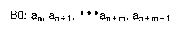
- a fourth CRC arithmetic unit 42 divides the second bit train B2, deemed to be the same bit train as the first bit train B1 with the same bit train as the bit train stored in the shift register 21 attached to the bottom thereof, by the generator polynomial G and deems the remainder obtained to be the fourth CRC arithmetic operation results C4. That is, the third CRC arithmetic unit 41 and the fourth CRC arithmetic unit 42 perform CRC arithmetic operations on the following B1 and B2 for the bit train comprised of a n . 2 , a n-1 , an, a n+1 ⁇ a n+m . 1 , a n + m , a n +m+1 :
- B2 " ⁇ an- 2 , an, a n+1 " a n+2 ⁇ a n+m-1 "
- the portions in the headers of the above-mentioned B1 and B2 start at the same time positions for both B1 and B2, for example, from ao or a 1 .
- the continuous CRC arithmetic unit 22 was formed based on the point expressed by the following equation:
- the CRC arithmetic operation results from an to a n+m-1 are C n and the generator polynomial used for the CRC arithmetic operations is G, they can be expressed by the above-mentioned equations (2) and (3).
- BO is equivalent to B2-B1.
- the first term on the right side (R[ ⁇ ] ⁇ of equation (12) shows the bit train B2, while the second term (-R[ ⁇ ]) shows the bit train B2.
- the header bits of the bit trains B1 and B2 are both at, so the bit trains start at the same time position.
- Figure 13 is a view of an example of realization of the second embodiment. As illustrated, it includes a m-bit shift register 21, the above-mentioned third CRC arithmetic unit 41 and fourth CRC arithmetic unit 42, and an EX-OR processing unit 44. The operation will be explained below:
- the third CRC arithmetic unit 41 is for performing the operation of the second term of the equation (12)
- the fourth CRC arithmetic unit 42 is for performing the operation of the first term of the equation (12).
- the addition and subtraction can be processed by EX-OR, so by finding the EX-OR of the operation results of the CRC arithmetic unit 41 and the CRC arithmetic unit 42 by the EX-OR processing unit 42, the target CRC arithmetic operation results C out sought can be obtained.
- Figure 14 is a view showing a first more detailed example of realization of the first embodiment.
- the CRC arithmetic unit 35 of Fig. 11 is shown as a ROM 35 in this figure. Further, the ROM 35 may be replaced with the parallel connection type of Fig. 3.
- Figure 15 is a view showing a second more detailed example of realization of the first embodiment.
- This second detailed example was based on the second conventional example (Fig. 2) mentioned earlier.
- the former (31) is an arithmetic unit with an and the latter (32) corresponds to the CRC arithmetic unit of Fig. 2.
- Figure 16 is a view showing a third more detailed example of realization of the first embodiment and is based on the construction of Fig. 15 with some modifications.
- the former (31) corresponds to the CRC arithmetic unit of Fig. 9 and the latter (32) is comprised of an R( ⁇ m/G) output unit.
- the R( ⁇ m/G) output unit 32 outputs the value of the above-mentioned equation (13) when an is “1 ". Therefore, D; outputs the truth value "1 " in accordance with R( ⁇ m/G) when the header of x i is “1" " and an is “1 ".
- reference numeral 13 is an EX-OR gate which obtains the EX-OR of the output of the shift register 12 and the corresponding output and D; of the connector 14 and outputs the result.
- Figure 17 is a view showing a first more detailed example of realization of the second embodiment.
- the CRC arithmetic units 41 and 42 of Fig. 13 use is made of the construction of the ROM 35 and the CRC memory unit 36 of Fig. 14.
- Figure 18 is a view showing a second more detailed example of realization of the second embodiment. Use is made of a CRC arithmetic unit 45 combining the two CRC arithmetic units 41 and 42 shown in Fig. 17. Note that as the ROM 35 of Fig. 17, use is made of the ROM 35' of a 21 +2 bit input and 21 bit output in Fig. 18.
- Figure 19 is a view showing a third more detailed example of realization of the second embodiment.
- the CRC arithmetic unit 41 of Fig. 13 use is made of the construction of Fig. 16, as the CRC arithmetic unit 42 of Fig. 13, use is made of the construction of Fig. 2, and as the EX-OR processing unit 44 of Fig. 13, use is made of the R( ⁇ m/G) output unit 46.
- the constants in Fig. 19 are the same as in the case explained for Fig. 16.
- Figure 20 is a view of a third embodiment according to the present invention.
- the continuous CRC arithmetic unit 22 includes a wired logic unit 51 and a remainder arithmetic unit 52.
- the wired logic unit 51 receives as input the m number of bit outputs b corresponding to the bits from the m-bit shift register unit 21 and distributes the m number of bit outputs b to predetermined bit positions set in advance for each of the m bits of output in the plurality of bit positions.
- the remainder arithmetic unit 52 is provided with a plurality of input gates 53 corresponding to the above-mentioned plurality of bit positions, executes the addition of the above-mentioned bit outputs b input distributed to each of the input gates 53, and calculates the remainder, which is equal to the remainder which would be obtained by dividing the input bit train B in by the generator polynomial G. This is given to the synchronization control unit 23 as the CRC arithmetic operation results C out .
- C( ⁇ ) is divided by the generator polynomial G( ⁇ ).
- Ep( x ) is a figure where only the coefficient of the term of the p-th order is 1 and the remainder are all 0 (see above-mentioned 1000 and 10).
- Equation (20) is the above-mentioned g.
- the remainder R( ⁇ ) obtained by dividing each of the above-mentioned Ep( ⁇ ) by the generator polynomial G( ⁇ ) is decided readily in advance, so by using this it is possible to make the wired logic unit 51 and the remainder arithmetic unit 52 extremely simple in construction and reduce the size of the hardware required.
- Figure 21 is a view of an example of realization of the third embodiment.
- the wired logic unit 51 is made of the wiring illustrated.
- Coo, C 01 ⁇ C 39 correspond to the above-mentioned C( x ).
- the output side of the wired logic unit 51 enters the input gates 53 of the remainder arithmetic unit 52.
- the input gates 53 are, for example, comprised of known parity check circuits (PC).
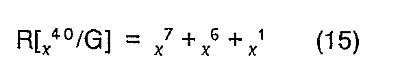
- the bits ( ⁇ 7, ⁇ 6 ⁇ x°) output from the parity check circuits PC become the CRC arithmetic operation results C out (corresponding to the above-mentioned R( x )) sought.
- this C out is input to the synchronization control unit 23.
- the wired logic unit 51 of Fig. 21 has its internal wiring determined by the calculation results. That is, as mentioned above, the remainder R( x ) obtained by dividing the above-mentioned E ⁇ ( ⁇ )'s one by one by the generator polynomial G( ⁇ ) is determined readily in advance, so this is used.
- Figure 22 is a view of the bit pattern for constituting the wired logic unit of Fig. 21.
- the monomials Ep( x ) are bit trains with just one of the 40 bits being “1” and the remainder all being “0", with the "1 bit differing in bit position.
- the "1" bits are arranged in a line slanting from the top left to the bottom right.
- the remainders R( ⁇ )'s obtained by dividing the values of the E ⁇ ( ⁇ )'s corresponding to x 39 , x 38 ⁇ ⁇ 00 by the generator polynomial G( ⁇ ) become the 8-bit bit trains shown in the right column of the figure. For example, for the term of x 39 , the remainder becomes: 00110001
- the horizontally extending wiring group and the parity check circuits (PC) receiving the same in the wired logic unit 51 in Fig. 21 are used to perform an operation equivalent to the addition of the bit trains in the right column of Fig. 22 in the lateral direction with the bit positions (j bits) matched and to obtain the desired remainder R( ⁇ ).
- Figure 23 is a view of a fourth embodiment according to the present invention.
- the continuous CRC arithmetic unit 22 is made of a remainder arithmetic unit 61 and a delay unit 62.
- the shift register unit 21 is comprised of a k-stage shift register. k is a specific number which is larger than 1 and smaller than the number of bits (for example, 8) making up one octet of the ATM cell.
- the bit output of the first stage of the k-stage shift register and the bit output of the k-th stage form two of the three inputs used for the CRC arithmetic operation in the remainder arithmetic unit 61.
- the remaining one input is the output from the delay unit 62.
- the remainder arithmetic unit 61 executes the predetermined operation receiving these three inputs and produces the CRC arithmetic operation results C out .
- the fourth embodiment is established taking note of a certain mathematical method which will be explained below. First, see Fig. 24.
- FIG 24 is a view of the general format of the ATM cell used for explaining the fourth embodiment.
- the figure shows the ATM cell shown in Fig. 9 with the header data in bit units. The following explanation will be made in terms of these bit units.
- ⁇ n is a numeral series expressed by eight factors: That is, if ⁇ n is expressed by a polynomial, the result is:
- ⁇ nx 8x4 corresponds to the first octet
- ⁇ n+1 ⁇ 8x3 corresponds to the second octet
- ⁇ and ⁇ n+4 ⁇ 8x0 corresponds to the fifth octet.
- Cn + can be expressed as follows:
- the CRC arithmetic operation results C n sought can be expressed extremely simply using the three elements C n . i , ⁇ n-1 , and ⁇ n+4 .
- These three elements are coefficients of X 8 , ⁇ 8x5 , and ⁇ 8x0 and occur at different times from each other, so when the remainder arithmetic unit 61 executes the arithmetic operations on the three elements, the three elements must be obtained at the same timing at the input of the remainder arithmetic unit 61.
- the k-stage shift register 21 and delay unit 62 shown in Fig. 23 exist for matching the above timings. Note that the three elements C n-1 , ⁇ n-1 , and ⁇ n+4 shown in the above-mentioned equation (28) appear at the portions shown in Fig. 23.
- Figure 25 is a view of an example of realization of the fourth embodiment.
- the k-stage shift register 21 is comprised of a 6-stage shift register (comprised of six flipflops FF connected in tandem).
- the above-mentioned element ⁇ n-1 is supplied from the first stage output receiving the input bit train B in , while the above-mentioned element ⁇ n+4 is supplied from the sixth stage output.
- These are applied to the remainder arithmetic unit 61.
- the other element C n - 1 to be input to the remainder arithmetic unit 61 is given from the delay unit 62.
- This may be comprised of a D-flipflop DFF as illustrated.
- the clock CLK defining the overall timing is, for example, a speed of 4M.
- the bit outputs Do, D 1 ⁇ D 5 are sent out from these FF's in synchronization with this. Further, the reset signal RST is given to the reset inputs of the FF's. The reset signal RST rises at the same time as the reception of the input bit train B in (see Fig. 26) and falls when the reception of B in is completed.
- Figure 26 is a timing chart of signals appearing at key portions of Fig. 25.
- the same references (CLK, B in ⁇ ) are given to the rows corresponding to the signals of Fig. 25.
- the downward facing arrow B in in the row of Do shows that the above-mentioned three elements ( ⁇ n-1 , ( ⁇ n+4 , C n - 1 ) are matched at the same time as ⁇ 5 , ⁇ 0 , and Co for the first time since being input.
- the CRC arithmetic operation results sought are C 1 .
- Figure 27 is a view of a detailed example of a remainder arithmetic unit.
- the remainder arithmetic unit 61 is comprised, for example, of the illustrated wired logic unit 63, the EX-OR gate 64, and 8- bit leading wires 65 for output of the CRC arithmetic operation results.
- the wired logic unit 63 receives at the input side the above-mentioned three elements ⁇ n+4 , ⁇ n-1 , and C n-1 as the bit outputs D 5 and Do of the 6-stage shift register 21 and the output of the delay unit 62 and is connected at the output side to eight EX-OR gates 64 (only three shown) corresponding to the eight bits.
- the wired logic unit 63 is assembled as shown in Fig.
- Figure 28 is a view of the bit pattern for constituting the portion corresponding to the bit output Do in the wired logic unit of Fig. 27
- Fig. 29 is a view of the bit pattern for constituting the portion corresponding to the bit output D 5 in the wired logic unit of Fig. 27
- Fig. 30 is a view of the bit pattern for constituting the portion corresponding to the immediately preceding CRC arithmetic operation result C n-1 in the wired logic unit of Fig. 27.
- the line connection corresponding to the "1" bit in the bit train of the order ⁇ 7 becomes the connection point A of the Do row in Fig. 27.
- the line connection corresponding to the "1" bit in the bit train of the order ⁇ 41 becomes the connection point B of the D ⁇ row of Fig. 27.
- the line connection corresponding to the "1" bit in the bit train of the order ⁇ 14 becomes the connection point C of the row C n-1 of Fig. 27.
- connection is made to the corresponding inputs of the EX-OR gate 64 made into bundles of eight corresponding to the 8 bits of the C n .
- the EX-OR gate performs an addition function and the results of the addition are sent out as Cn to the leading wires 65 corresponding to the bits.
- the synchronization circuit (20 in Fig. 8) When the synchronization circuit (20 in Fig. 8) is actually used in an ATM communication system, the synchronization circuit provided at the side receiving the ATM cells must function to provide rear protection and front protection as well. That is, the synchronization control unit (23 in Fig. 8) must include a rear protection and front protection means. Usually, rear protection is provided seven times and front protection six times.
- the synchronization circuit 20 of the present invention is preferably provided with a rear protection and front protection function.
- Figure 31 is a block diagram of the principle of a synchronization circuit including a reset means.
- the synchronization circuit 20 in the figure is provided with a reset means 70 at the synchronization control unit 23 at the reception side.
- the reset signal R/S from the reset means 70 is applied to the shift register unit 21 and the continuous CRC arithmetic unit 22.
- the rear protection function and the front protection function can be started up at cycles of 53 bytes (53 octets).
- the synchronization circuit of the present invention would not function with just the synchronization detection started up every 53 bytes.
- the synchronization circuit 20 has the shift register unit 21 with the data holding function and the CRC arithmetic unit 22 (CRC memory unit 36 and delay unit 62). That is, it is necessary to reset the past data remaining in the data holding function unit. Therefore, the reset means 70 is provided. This reset means 70 is essential for performing the rear protection and front protection. A detailed example will be provided below:
- Figure 32 is a view of an example of application of the reset means to the synchronization circuit of Fig. 14. The operation in the figure is as follows: Here, the ROM 35 has written in it the results of calculation of the C n + from an, a n + 40 , and C n in advance.
- the synchronization detection signal S d is output from the synchronization control unit 23 in the state where the conditions for front protection for synchronization have been met.
- the set signal is output from the synchronization control unit 23.
- the CRC arithmetic processing unit is set to a state waiting for the same meaning as the internal state desired in the synchronization state (shift register - all "0", CRC memory unit - all "0").
- Figure 33 is a view of an example of a synchronization control unit 23 in Fig. 32. This includes a reset means 70.
- Figure 34 is a timing chart showing the reset signal in Fig. 33. 424 in the figure means 53 (all octets in ATM cell) x 8 (bits) and 40 means 5 (all octets of header in ATM cell) x 8 (bits).
- the reset signal R/S is output cyclically as illustrated and is output to the CRC arithmetic processing unit 71 (Fig. 32).
- the hunt processing unit 72 is in a hunting state.
- the CRC arithmetic processing unit 71 starts the CRC arithmetic operation and C n 's are successively input to the comparator unit 24.
- the comparator unit 24 when C n matches the desired value, the coincidence signal is output. At this time, the signal PS showing that the pseudo synchronization has started is output from the hunt processing unit 72, and the rear protection operation is started at the rear protection unit 73.
- the rear protection unit 73 which starts the rear protection operation checks that the coincidence signal is received successively seven times for each 53 bytes from the point of time when the signal PS is input. At this time, the synchronization start signal SS is output to the front protection unit 74.
- the synchronization state exists while the coincidence signal is input to the front protection unit 74 every 53 bytes.
- the front protection unit 74 When the coincidence signal coming every 53 bytes stops, the front protection unit 74 enters the front protection state. At this time, just the synchronization detection signal Sd is output every 53 bytes. When the coincidence signal is not input for six successive times, the front protection unit 74 outputs the reset signals R1 and R/S and the above-mentioned state (1) is returned to. When the coincidence signal is once again input in the 53 x i (i ⁇ 6) byte, the above-mentioned state (4) is returned to.
- Figure 35 is a view of an example of incorporation of the reset means in the circuit of Fig. 25.
- the reset means 70 executes the CRC arithmetic operation on the 5 octets from the header every 53 octets (length of one ATM cell) and is essential for the rear protection and front protection.
- a detailed example was given in Fig. 32.
- the second detailed example shown in Fig. 35 has a reset means 70 built in the synchronization circuit of Fig. 25.
- the reset means 70 can be extremely easily realized by an AND gate 75. This is also an advantage of the synchronization circuit of Fig. 25.
- the AND gate 75 receives as input the above-mentioned reset signal RST and the output H of a header counter (not shown) and outputs the reset signal R/S.
- the reset signal R/S is applied to the sixth stage flipflop FF and the reset inputs of the flipflop forming the delay unit 62.
- the above-mentioned header counter produces a cyclic output H synchronized with 53 octets. The waveform is shown in the row H of Fig. 36.
- Figure 36 is a timing chart of signals appearing at key portions of Fig. 35.
- the synchronization control unit 23 in the synchronization circuit 20 is provided with a header error correction means in addition to the above-mentioned reset means 70.
- a header error correction means suitable for being incorporated in the synchronization control unit 23 is shown.
- the header error correction means enters the active state after the synchronization circuit enters the synchronization state through the above-mentioned rear protection. Strictly speaking, this is the synchronization state when there is no error in the header of the ATM cell appearing just before. Therefore, consider the definite time series ⁇ :
- ( ⁇ +E)' can be rewritten to the following equation: Therefore, the syndrome S' for this ( ⁇ + E)' becomes: The term of ( ⁇ i ⁇ )mod( ⁇ 127 -1 in the above does not include an error, so is 0.
- S in equation (40) shows the initial state of the data and may be illustrated as follows: Note that [1] to [5] correspond to the first octet to fifth octet of the header of the ATM cell. Further, the code length is 127 bits.
- Figure 43 is a view of an example of the bit correction unit of Fig. 37.
- Figure 44 is a timing chart of signals appearing at key portions of Fig. 43.
- 91 is an arithmetic circuit
- 92 to 94 are flipflops
- 95 is an EX-OR gate.
- a header error is detected at the stage in front of the block 89 in Fig. 37. After this, the error is corrected by the bit correction unit 89 of Fig. 43 by the operation of Fig. 44.
- the header error correction here, by obtaining the EX-OR E of the data when Si has a one-bit error and ⁇ i by the EX-OR gate 95, the corrected data bit T is obtained.
- the arithmetic circuit 91 consideration will be given to the arithmetic circuit 91.
- the arithmetic circuit 91 The arithmetic circuit 91
- the output R c of the arithmetic circuit 91 becomes the logical OR output of the above-mentioned R ca and R cb .
- the ATM cells are continuously sent in from the transmission side on the transmission channel. If this transmission channel is disconnected, the all "0" or all “1” data appears at the reception side. If the all "0" data appears, the CRC arithmetic operation result also becomes “0" and the reception side enters a state equivalent to one where synchronization is established. This is the pseudo synchronization detection state.
- an offset bit train be mapped at the HEC region (HEC in Fig. 9) in the header of the ATM cells at the transmission side in advance.
- This offset bit train would, for example, be as follows:
- Figure 45 is a block diagram of the principle of a synchronization circuit including a logic inversion means.
- Reference numeral 100 in the figure is a logic inversion means.
- the bit corresponding to the CRC arithmetic operation result is inverted in logic.
- the bit corresponding to the CRC arithmetic operation result is passed with its logic as is. Showing this operation by a numerical equation, looking at the above-mentioned equation (17),
- Figure 46 is a view of an example of a logic inversion means.
- the logic inversion means 100 is applied to the continuous CRC arithmetic unit 22 of Fig. 21 (third embodiment).
- the logic inversion means of Fig. 45 is comprised of a group of invertors 101.
- the invertor 101 is connected at the bit position corresponding to "1 " in the above-mentioned offset bit train.
Landscapes
- Engineering & Computer Science (AREA)
- Computer Networks & Wireless Communication (AREA)
- Signal Processing (AREA)
- Error Detection And Correction (AREA)
- Synchronisation In Digital Transmission Systems (AREA)
- Detection And Correction Of Errors (AREA)
- Data Exchanges In Wide-Area Networks (AREA)
Abstract
Description
- The present invention relates to a synchronization circuit, in particularly a synchronization circuit in an asynchronous transfer mode (ATM) communication system for synchronization of ATM cells connected on the lines in the system, that is, cell synchronization.
- At the present time, the CCITT is proposing ATM communications suitable for broad band ISDN's etc., that is, data transfer by an asynchronous transfer mode, and is pressing forward with standardization of such systems. One proposal is for use of a full ATM for a
layer 1. - If full ATM is used for the
layer 1 in accordance with that proposal, technology would become necessary for extracting each and every ATM cell, the units of data transferred by the ATM communications network. That is, it would be necessary to establish cell synchronization and detect the positions of the cells (extraction of the cells). - To extract cells in this way, cyclic redundancy check (CRC) arithmetic operations are said to be extremely effective. That is, the CRC arithmetic operation is performed on the header of a cell, the cells are detected when the results of the CRC arithmetic operation become fixed values, and cell synchronization is performed. In this case, even detection of errors of the cell header itself can naturally be performed by the inherent CRC function. Note that even when an error is included in a cell, cell synchronization can be sufficiently ensured by so-called front protection and rear protection.
- Usually, ATM cells are comprised of the above header and a payload for transmitting the inherent information. The header also includes a field known as a header error control (HEC). The result of the CRC arithmetic operation are written into this HEC. The present invention relates to a synchronization circuit which writes, at the transmission side of the ATM cell, the result of the CRC arithmetic operation on the header in the HEC as a cell synchronization establishment signal and detects, at the reception side of the ATM cell, the coincidence of the results of the CRC arithmetic operation on the header of the ATM cell received and the result of the CRC arithmetic operation written at the transmission side in the HEC of the ATM cell received so as to detect if cell synchronization has been achieved and outputs a synchronization detection signal.
- A detailed explanation will be made later of several conventional CRC arithmetic units referring to the attached figures. Here, in summary, however, conventional CRC arithmetic units basically are constructed to receive input bit trains having definite time series, perform CRC arithmetic operations on the trains, and obtain a CRC arithmetic operation result.
- On the other hand, in the ATM transmission art, a synchronization circuit of the full ATM transmission system does not cover such input bit trains having definite time series, but cover input bit trains having indefinite time series (ATM cell groups), so it is necessary to shift the input bit trains one bit at a time to continuously obtain CRC arithmetic operation results Couto
- If a conventional CRC arithmetic unit is assembled and designed to perform a CRC arithmetic operation on such input bit trains having indefinite time series (ATM cell groups), the assembled CRC arithmetic operation circuit would enlarge the size of the apparatus (hardware). Further, if the CRC arithmetic operation is performed on ultrahigh speed data, the problem will arise of an increased processing delay.
- Therefore, the present invention, in view of the above-mentioned problems, has as its object the provision of a synchronization circuit provided with a CRC arithmetic unit which can obtain continuous CRC arithmetic operation results from input bit trains comprised of indefinite time series without increasing the processing delay and without increasing the size of the apparatus even in the case of ultrahigh speed data of several 100 Mb/s or more.
- To attain the above object, the synchronization circuit of the present invention includes a shift register unit, a continuous CRC arithmetic unit, and a synchronization control unit. The shift register unit receives and holds in a bit serial form the input bit trains comprising the ATM cells provided for the data transfer. The continuous CRC arithmetic unit performs the CRC arithmetic operation in accordance with a simplified CRC arithmetic operation process comprising a conventional CRC arithmetic operation process modified in advance to reduce the amount of operations. The synchronization control unit receives as input the CRC arithmetic operation result from the continuous CRC arithmetic unit. On the transmission side of the ATM cells, it inserts the CRC arithmetic operation result in the ATM cells as the synchronization establishment signal and sends the same, while on the reception side of the ATM cells, it outputs a synchronization detection signal when the CRC arithmetic operation result transmitted from the transmission side and the CRC arithmetic operation result obtained by the operations of the continuous CRC arithmetic unit on the reception side coincide.
- The above objects and features of the present invention will be more apparent from the following description of the preferred embodiments with reference to the accompanying drawings, wherein:
- Fig. 1 is a view of a first example of a conventional CRC arithmetic unit;
- Fig. 2 is a view of a second example of a conventional CRC arithmetic unit;
- Fig. 3 is a view of an example of an improvement of the first example of the conventional CRC arithmetic unit;
- Fig. 4 is a view of an input bit train having a definite time series;
- Fig. 5 is a view of an input bit train having an indefinite time series;
- Fig. 6 is a view of a first example of a synchronization circuit handling input bit trains having indefinite time series;
- Fig. 7 is a view of a second example of a synchronization circuit handling input bit trains having indefinite time series;
- Fig. 8 is a block diagram of the principle of the synchronization circuit according to the present invention;
- Fig. 9 is a view of the general format of an ATM cell to which the present invention is applied;
- Fig. 10 is a view of a first embodiment of the present invention;
- Fig. 11 is a view of an example of realization of the first embodiment;
- Fig. 12 is a view of a second embodiment according to the present invention;
- Fig. 13 is a view of an example of realization of the second embodiment;
- Fig. 14 is a view showing a first more detailed example of realization of the first embodiment;
- Fig. 15 is a view showing a second more detailed example of realization of the first embodiment;
- Fig. 16 is a view showing a third more detailed example of realization of the first embodiment;
- Fig. 17 is a view showing a first more detailed example of realization of the second embodiment;
- Fig. 18 is a view showing a second more detailed example of realization of the second embodiment;
- Fig. 19 is a view showing a third more detailed example of realization of the second embodiment;
- Fig. 20 is a view of a third embodiment according to the present invention;
- Fig. 21 is a view of an example of realization of the third embodiment;
- Fig. 22 is a view of the bit pattern for constituting the wired logic unit of Fig. 21;
- Fig. 23 is a view of a fourth embodiment according to the present invention;
- Fig. 24 is a view of the general format of the ATM cell used for explaining the fourth embodiment;
- Fig. 25 is a view of an example of realization of the fourth embodiment;
- Fig. 26 is a timing chart of signals appearing at key portions of Fig. 25;
- Fig. 27 is a view of a detailed example of a remainder arithmetic unit;
- Fig. 28 is a view of the bit pattern for constituting the portion corresponding to the bit output DO in the wired logic unit of Fig. 27;
- Fig. 29 is a view of the bit pattern for constituting the portion corresponding to the bit output D5 in the wired logic unit of Fig. 27;
- Fig. 30 is a view of the bit pattern for constituting the portion corresponding to the immediately preceding CRC arithmetic operation result Cn-1 in the wired logic unit of Fig. 27;
- Fig. 31 is a block diagram of the principle of a synchronization circuit including a reset means;
- Fig. 32 is a view of an example of application of the reset means to the synchronization circuit of Fig. 14;
- Fig. 33 is a view of an example of a
synchronization control unit 23 in Fig. 32; - Fig. 34 is a timing chart showing the reset signal in Fig. 33;
- Fig. 35 is a view of an example of incorporation of the reset means in the circuit of Fig. 25;
- Fig. 36 is a timing chart of signals appearing at key portions of Fig. 35;
- Fig. 37 is a view of a specific example of a header error correction means;
- Fig. 38 is a timing chart of signals appearing at key portions of Fig. 37;
- Fig. 39 is a view of an example of an S-1 arithmetic unit in Fig. 37;
- Fig. 40 is a view of the bit pattern for constituting the S-1, arithmetic unit of Fig. 39;
- Fig. 41 is a view of one example of the Si, arithmetic unit in Fig. 37;
- Fig. 42 is a view of the bit pattern for constituting the Si arithmetic unit in Fig. 41;
- Fig. 43 is a view of an example of the bit correction unit of Fig. 37;
- Fig. 44 is a timing chart of signals appearing at key portions of Fig. 43;
- Fig. 45 is a block diagram of the principle of a synchronization circuit including a logic inversion means; and
- Fig. 46 is a view of an example of a logic inversion means.
- Before describing the embodiments of the present invention, the related art and the disadvantageous therein will be described with reference to the related figures.
- First, an explanation will be made of the conventional CRC arithmetic unit used for the previously mentioned CRC arithmetic operations. Figure 1 is a view of a first example of a conventional CRC arithmetic unit.
- The first conventional example (Fig. 1) is of a type which reads out the CRC arithmetic operation results by a table and includes a
ROM 11 storing the table, that is, a ROM table. - All CRC arithmetic operation results Cout for the bit trains B;n of the input m number of bits are stored in advance in the ROM table. The input bit trains Bin are considered as addresses of the
ROM 11 and the data read out at this time is the CRC arithmetic operation result sought. - Figure 2 is a view of a second example of a conventional CRC arithmetic unit.
- The second conventional example (Fig. 2) is of a so-called shift register type and includes serially connected shift registers 12 and exclusive OR gates (EX-OR) 13 inserted between the shift registers. The exclusive OR
gates 13 haveconnectors 14 connected to them. Theconnectors 14 connect or do not connect (truth value set to "0") the CRC arithmetic operation results Cout' in accordance with the coefficients of each order of the general polynomials used in the CRC arithmetic operation ("1" or "0"). Subtraction by theEX-OR 13 is not performed when the coefficient is "0". - Therefore, at the initial state, the values of all
shift registers 12 are cleared to "0", then bit trains are successively input from the left side of the figure. The values of all shift registers 12 (χ0,χ1... xn.1) when the final bit is input to the shift register 12 (xo) at the left side show the CRC arithmetic operation result sought. Therefore, the values of χo to χn-1 are read out at that point of time and the arranged value Cout is the value sought. - Figure 3 is a view of an example of an improvement of the first example of the conventional CRC arithmetic unit.
- The improved version of the first example of the conventional CRC arithmetic unit is a type which reads out the CRC arithmetic operation result and is comprised of a combination of a plurality of ROM tables and a plurality of EX-OR logic gates, with a plurality of ROM's 11 and a plurality of exclusive OR gates (EX-OR) 13 being connected in parallel as illustrated. The contents of these ROM's 11 differ, however, so the ROM's are referred to as the
ROM 1,ROM 2•••.For example, theROM 1 contains arithmetic operation results of "XXX•••X 000•••0"(XXX•••X being the «1 bit and 000··· 0 being the m-α1 bit), theROM 2 contains the arithmetic operation result of "XXX•••X 0000" (XXX•••X being the α2 bit and 000···0 being the m-α1-α2 bit). - The bit train B;n of the input m number of bits is divided into suitable numbers of bits (shown by α1, α2···αp, for example, each comprised of five bits). The CRC arithmetic operation result read out from the corresponding ROM 11 (each being of 1 number of bits) are input to the EX-OR's 13 as illustrated. The CRC arithmetic operation result Cout sought is obtained from the
final stage EX-OR 13. Note that when the number of bits of the remaining αp+1 bits is smaller than the number of bits of the generator polynomial, αp+1 is input to the final stage EX-OR 13 as is as the remainder. - According to this improved example, even if the number of bits m increases, the address space sought in the
ROM 11 does not increase exponentially as in the first conventional example (Fig. 1). Further, compared with the above-mentioned second conventional example, since the CRC arithmetic operation processing is parallel processing, there is the advantage that a high speed is not required in the logic devices (ROM 1 and EX-OR 13). - The examples of the CRC arithmetic units given above are convenient for performing CRC arithmetic operations on segmented bit trains formed by dividing a continuous bit train into certain bit lengths. That is, they are suitable for CRC arithmetic operations on input bit trains having definite time series.
- Figure 4 is a view of an input bit train having a definite time series. In this figure, for example, a bit train Bin divided into lengths of m bits is shown. It shows in particular the q-th segmented bit train and the q+1- st segmented bit train.
- Figure 5 is a view of an input bit train having an indefinite time series. The figure shows the state of shifting the object of the CRC arithmetic operation one bit at a time. That is, the extraction of a cell at the full ATM mentioned above is performed by successively shifting the input bit train Bin by a bit and executing a CRC arithmetic operation each time. The figure shows the input bit train Bin covered by the q-th, q + 1-st, and q + 2-nd CRC arithmetic operations.
- Figure 6 is a view of a first example of a synchronization circuit handling input bit trains having indefinite time series.
- Figure 7 is a view of a second example of a synchronization circuit handling input bit trains having indefinite time series. Continuously sought CRC arithmetic operation results Cout are obtained from these circuits. Note that Cp, Cp+1 ·· in Fig. 7 are issued at respectively inherent timings and all form the Cont.
- The first example of the circuit (Fig. 6) corresponds to one based on the improvement of the first conventional example mentioned earlier (Fig. 3) and includes a multiple
stage shift register 12 and aCRC arthmitic unit 16. Th CRCarithmetic unit 16 is basically the same in circuit construction as the ones shown in Fig. 1 and Fig. 3. - The second example of the circuit (Fig. 7) includes a number of CRC
arithmetic units 17 provided in parallel and acontrol apparatus 18 for controlling the same. Thearithmetic units 17 are basically the same in construction as the fore-mentioned second conventional example (Fig. 2). - However, when the first conventional example (Fig. 1) is used, an increase in the number of bits m is accompanied by an exponential increase in the address space in the
ROM 11 and the problem occurs of a large size of the hardware. When the improvement (Fig. 3) is used, EX-OR's 13 are connected to numerous stages and the operating speed of thelayer 1 of the ATM is 620 Mb/s or 155 Mb/s, so the gate (EX-OR) delay during the processing becomes a problem. - On the other hand, the second conventional example (Fig. 2) is constructed so that the results appear at the point of time when the input of m bits has ended, so the second example of the circuit (Fig. 7) requires a plurality of CRC
arithmetic units 17, resulting in the problems of an increased size of hardware and the need for thecontrol apparatus 18. - Below, an explanation will be given on the synchronization circuit of the present invention, which can resolve the above-mentioned problems.
- Figure 8 is a block diagram of the principle of the synchronization circuit according to the present invention. In the figure, the
synchronization circuit 20 according to the present invention includes ashift register unit 12, a continuous CRCarithmetic unit 22, and asynchronization control unit 23. - The
shift register unit 21 receives and holds in a bit serial fashion the input bit train Bn constituting the ATM cell (Fig. 9) supplied for the data transmission. - The continuous CRC
arithmetic unit 22 performs CRC arithmetic operations in accordance with a modified CRC arithmetic operation process comprised of the usual CRC arithmetic operation process modified to reduce the amount of operations. - The
synchronization control unit 23 receives as input the CRC arithmetic operation result Cout from the continuous CRCarithmetic unit 22, inserts, at the transmission side of the ATM cell, the CRC arithmetic operation result Cout as the synchronization establishment signal Se in the ATM cell and transmits the same and, at the reception side of the ATM cell, outputs a synchronization detection signal Sd when the CRC arithmetic operation result Cout sent from the transmission side and the CRC arithmetic operation result Cout obtained by operations of the continuous CRCarithmetic unit 22 at the reception side coincide. - Figure 9 is a view of the general format of an ATM cell to which the present invention is applied. In the figure, the 1, 2, 3"' 8 at the top show the bit positions from the LSB (1) to the MSB (8), and the 1, 2, 3... 53 at the right side are octets showing the divisions in the ATM cell (hereinafter simply referred to as "cell"). The cell is divided into a header and a payload (data in the cell). VPI (virtual path identifier) and VCI (virtual circuit identifier) show destinations of the cell. CLP is the cell loss priority. Among these, VPI1 is part of the VPI at NNI and includes information for cell conflict control, known as GFC, when UNI. The previously mentioned HEC is the portion for monitoring the header as a whole.
- The cell of the structure shown in Fig. 9 continuously flows along the transmission path of the ATM communication network in the order of the first octet MSB -> LSB and second octet MSB -> LSB. The HEC covers from the first octet to the fourth octet. If a CRC arithmetic operation including the HEC is performed, the CRC arithmetic operation results Cout should be all "0" if the cell is normal. Further, the generator polynomial used is, for example,

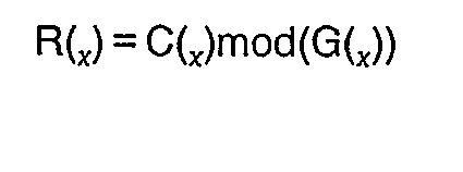
- The usual CRC arithmetic operation process, mentioned earlier, is as follows: For an input bit train Bin of a certain time series:


modulo 2 operation, which is mathematically expressed as R(f/g)=fmod(g). - Usually, the amount of operations required for the above function R (f/g) is tremendous, therefore the hardware required for the CRC arithmetic operation becomes large in size and the above-mentioned problem occurs. The present invention greatly reduces the amount of the operations by the
shift register unit 21 and the continuous CRCarithmetic unit 22. - Figure 10 is a view of a first embodiment of the present invention. In the figure, the first
CRC arithmetic unit 31 deems the overflow bit (B1) forced out from theshift register unit 21 to be a term of the m-th order, divides this term of the m-th order by the generator polynomial used for the CRC arithmetic operation, and deems the remainder to be the first CRC arithmetic operation result C1. - The second
CRC arithmetic unit 32 deems the bit appearing at the second bit train B2 side at the same time as the overflow bit B1 is forced out to be the term of the 0-th order, adds the 0-th order term and the remainder after dividing the immediately preceding CRC arithmetic operation result Cout by the generator polynomial G, and uses the value as the second CRC arithmetic operation result C2. - The difference between the C1 and C2 is then taken by the
subtraction unit 33 and is used as the CRC arithmetic operation result Cout sought. - In the above first embodiment, the continuous CRC
arithmetic unit 22 was formed based on the point expressed by the following equation: - Referring once again to the above-mentioned equation (2) and equation (3), first the CRC arithmetic operation result Cn+1 obtained after shifting the Cn in equation (2) by one bit is


- The first term is the
remainder 0, so this is deleted and

- The Cn in the operator of the first term corresponds to the value from the feedback line of Fig. 10. The operation of the second term relates to the
arithmetic unit 31 and the operation of the third term relates to thearithmetic unit 32. Note that the third term is of a lower order than the generator polynomial G and in actuality is in itself immediately the remainder, so the following expression is possible:
- Equation (7) means that to find Cn+1, one may perform a CRC arithmetic operation on

- Further, equation (9) means that to find Cn+1, one may
- [1] perform a CRC arithmetic operation on Cn,,
- [2] subtract the results of the CRC arithmetic operation on anχ m, and
- [3] add an+mχ0.
- Here, [1] is possible even in the first conventional example (Fig. 1) since the number of bits is small and further, since continuous processing is possible, is possible in the second conventional example (Fig. 2) as well. [2] gives figures which are known in advance since when an is "0", the operation results are all "0" and when an is "1 ",the operation results are

- If the first embodiment is more practically constructed, it becomes as shown in Fig. 11.
- Figure 11 is a view of an example of realization of the first embodiment. As illustrated, this includes an m-
bit shift register 21, a CRCarithmetic unit 35, and aCRC memory unit 36. The operation will be explained below: - i) In the initial state (state where the data bit train Bin is not input to the continuous CRC arithmetic unit 22), the
shift register 21 and theCRC memory unit 36 are reset to all "0". - ii) In the state after the initial state, a1 is input to the LSB of the
shift register 21 and the CRCarithmetic unit 35. At this time, in theshift register 21, the data is shifted in direction from the LSB to the MSB. Further, at this time, at the same time, the CRC arithmetic operation result of the state just before (initial state), that is, the all "0" state, from theCRC memory unit 36 and the "0" from the MSB (output) of theshift register 21 are input to the CRCarithmetic unit 35. In this state, the CRCarithmetic unit 35 determines the next CRC arithmetic operation value and sets it in theCRC memory unit 36. - iii) In the state after ii), a2 is input to the LSB (input) of the
shift register 21 and the CRCarithmetic unit 35. At this time, in theshift register 21, the data is shifted in the direction from the LSB to the MSB. Further, at this time, at the same time, the CRC arithmetic operation value of the state just before (above i) from theCRC memory unit 36 and the "0" from the MSB of theshift register 21 are input to the CRCarithmetic unit 35. In this state, the CRCarithmetic unit 35 determines the next CRC arithmetic operation value and sets it in theCRC memory unit 36. - iv) When am+1 is to be input, am + is input to the LSB (input) of the
shift register 21 and the CRCarithmetic unit 35. At this time, in theshift register 21, the data is shifted in the direction from the LSB to the MSB. Further, at this time, at the same time, the CRC arithmetic operation value of the state just before from theCRC memory unit 36 and the a1 from the MSB of theshift register 21 are input to the CRCarithmetic unit 35. In this state, the CRCarithmetic unit 35 determines the next CRC arithmetic operation value and sets it in theCRC memory 36. - v) In the usual state, Cn (CRC arithmetic operation result from an to an+m+i) is stored. At this point of time, the next data an+m is input to the LSB (input) of the
shift register 21 and the CRCarithmetic unit 35. At this time, in theshift register 21, the data is shifted in the direction from the LSB to the MSB. Further, at this time, at the same time, the Cn from theCRC memory unit 36 and the an from the MSB of theshift register 21 are input to the CRCarithmetic unit 35. In this state, the CRCarithmetic unit 35 determines the next CRC arithmetic operation value Cn+1 and sets it in theCRC memory unit 36. - The CRC arithmetic operation of the first embodiment (Fig. 10) mentioned above may be summarized as follows:
- The
shift register unit 21 gives a delay of a length of m bits to the input bit train Bin. - The first
CRC arithmetic unit 31 fetches the first bit train B1 forced out from theshift register unit 21 and performs the first CRC arithmetic operation. - The second
CRC arithmetic unit 32 fetches the second bit train B2 divided at the input stage of theshift register unit 21 and performs the second CRC arithmetic operation. - The
subtraction unit 33 finds the difference between the first CRC arithmetic operation results C1 and the second CRC arithmetic operation results C2 from the firstCRC arithmetic unit 31 and the secondCRC arithmetic unit 32. The CRC arithmetic operation result Cout is obtained from thesubtraction unit 33 in a time series. - The continuous CRC
arithmetic unit 22 of the present invention, referring to Fig. 5, when performing a CRC arithmetic operation of the q + 1-st bit train, shifts the bits at the q + 1-st place and thereby matches the past bit excluded from the q-th bit train (or the bit train) and the newly entered current bit (or bit train) at the same timing, performs the CRC calculation, and sends out the difference of the CRC arithmetic operation results continuously for each bit. - Figure 12 is a view of a second embodiment according to the present invention. In the figure, a third CRC
arithmetic unit 41 divides the first bit train B1, which has been delayed by m bits and deemed as the m-th order term, by the generator polynomial used for the CRC arithmetic operation and deems the remainder obtained to be the third CRC arithmetic operation results C3. - A fourth CRC
arithmetic unit 42 divides the second bit train B2, deemed to be the same bit train as the first bit train B1 with the same bit train as the bit train stored in theshift register 21 attached to the bottom thereof, by the generator polynomial G and deems the remainder obtained to be the fourth CRC arithmetic operation results C4. That is, the third CRCarithmetic unit 41 and the fourth CRCarithmetic unit 42 perform CRC arithmetic operations on the following B1 and B2 for the bit train comprised of an.2, an-1, an, an+1··· an+m.1, an+m, an+m+1: - B1: "·· an-2, an00000···0" (wherein there are m number of 0's)
- B2: "··· an-2, an, an+1" an+2··· an+m-1" Here, the portions in the headers of the above-mentioned B1 and B2 start at the same time positions for both B1 and B2, for example, from ao or a1.
- The difference between C3 and C4 is obtained by the
subtraction unit 43 and is used as the CRC arithmetic operation result sought. - In the above-mentioned second embodiment, the continuous CRC
arithmetic unit 22 was formed based on the point expressed by the following equation: - In the same way as explained with regard to the first embodiment, if, for an input bit train Bin of a certain time series:

- The CRC arithmetic operation results from an to an+m-1 are Cn and the generator polynomial used for the CRC arithmetic operations is G, they can be expressed by the above-mentioned equations (2) and (3).
- At this time, Cn is expressed as


- The principle of derivation of this equation (12) is as follows:
- Consider the bit train of at, at+1, ···an-1, an, an+1, ···an+m, an+m+1 divided into the following two bit trains:
- B1: at' at+1, ···an-1, 0,0,0···0 (wherein there are m number of 0's)
- B2: at, at+1, ·· an, an+1, ···an+m, an+m+1 Equation (12) originally covered the following bit train:
- Therefore, BO is equivalent to B2-B1. Here, the first term on the right side (R[····· ]} of equation (12) shows the bit train B2, while the second term (-R[······]) shows the bit train B2. Here, the header bits of the bit trains B1 and B2 are both at, so the bit trains start at the same time position.
- If the second embodiment is constructed more practically, the result is Fig. 13.
- Figure 13 is a view of an example of realization of the second embodiment. As illustrated, it includes a m-
bit shift register 21, the above-mentioned third CRCarithmetic unit 41 and fourth CRCarithmetic unit 42, and anEX-OR processing unit 44. The operation will be explained below: - The third CRC
arithmetic unit 41 is for performing the operation of the second term of the equation (12), and the fourth CRCarithmetic unit 42 is for performing the operation of the first term of the equation (12). In modulo 2 operations, the addition and subtraction can be processed by EX-OR, so by finding the EX-OR of the operation results of the CRCarithmetic unit 41 and the CRCarithmetic unit 42 by theEX-OR processing unit 42, the target CRC arithmetic operation results Cout sought can be obtained. - It is possible therefore to continuously obtain CRC arithmetic operation results for input bit trains having indefinite time series while shifting by one bit at a time and the extraction of cells under the above-mentioned full ATM can be easily realized.
- Below, detailed examples will be given of the above-mentioned first embodiment and second embodiment.
- Figure 14 is a view showing a first more detailed example of realization of the first embodiment. The CRC
arithmetic unit 35 of Fig. 11 is shown as aROM 35 in this figure. Further, theROM 35 may be replaced with the parallel connection type of Fig. 3. In the example of Fig. 14, m = 40 bits and 1 (remainder) = 8 bits. 40 = 8 bits x 5 octets. - Figure 15 is a view showing a second more detailed example of realization of the first embodiment. This second detailed example was based on the second conventional example (Fig. 2) mentioned earlier. Among the first and second CRC
arithmetic units - The
arithmetic unit 31 with an mentioned above finds the EX-OR of
shift register 12. Note that theEX-OR gate 13 andconnector 14 are as previously explained. In the example of Fig. 15, m = 40 bits and 1 = 8 bits and
connector 14 are connected while the "3","4", "5", "6", and "7" of the connector 14 (not shown in the figure) are not connected and are fixed at "0". - Figure 16 is a view showing a third more detailed example of realization of the first embodiment and is based on the construction of Fig. 15 with some modifications. Of the first and second CRC
arithmetic units - The R(χm/G)
output unit 32 outputs the value of the above-mentioned equation (13) when an is "1 ". Therefore, D; outputs the truth value "1 " in accordance with R(χm/G) when the header of xi is "1" " and an is "1 ". Further,reference numeral 13 is an EX-OR gate which obtains the EX-OR of the output of theshift register 12 and the corresponding output and D; of theconnector 14 and outputs the result. - Here, the constants are the same as in the case of the above-mentioned second detailed example (Fig. 15). Regarding Di,
- Figure 17 is a view showing a first more detailed example of realization of the second embodiment. As the CRC
arithmetic units ROM 35 and theCRC memory unit 36 of Fig. 14. - Figure 18 is a view showing a second more detailed example of realization of the second embodiment. Use is made of a CRC
arithmetic unit 45 combining the two CRCarithmetic units ROM 35 of Fig. 17, use is made of the ROM 35' of a 21 +2 bit input and 21 bit output in Fig. 18. - Figure 19 is a view showing a third more detailed example of realization of the second embodiment. As the CRC
arithmetic unit 41 of Fig. 13, use is made of the construction of Fig. 16, as the CRCarithmetic unit 42 of Fig. 13, use is made of the construction of Fig. 2, and as theEX-OR processing unit 44 of Fig. 13, use is made of the R(χm/G)output unit 46. The constants in Fig. 19 are the same as in the case explained for Fig. 16. - Figure 20 is a view of a third embodiment according to the present invention. In the figure, the continuous CRC
arithmetic unit 22 includes a wiredlogic unit 51 and a remainderarithmetic unit 52. The wiredlogic unit 51 receives as input the m number of bit outputs b corresponding to the bits from the m-bitshift register unit 21 and distributes the m number of bit outputs b to predetermined bit positions set in advance for each of the m bits of output in the plurality of bit positions. Theremainder arithmetic unit 52 is provided with a plurality ofinput gates 53 corresponding to the above-mentioned plurality of bit positions, executes the addition of the above-mentioned bit outputs b input distributed to each of theinput gates 53, and calculates the remainder, which is equal to the remainder which would be obtained by dividing the input bit train Bin by the generator polynomial G. This is given to thesynchronization control unit 23 as the CRC arithmetic operation results Cout. - The third embodiment was established taking note of a mathematical method. The explanation of this mathematical method would be somewhat complicated, so first the general image will be briefly explained.
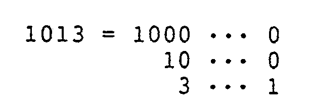
- Assume that remainder (R) obtained by dividing the decimal number "1013" (corresponding to the input bit train Bin) by "2" (corresponding to the generator polynomial G) is usually found by the process as follows:

- Taking note of a certain mathematical property, however, it is possible to similarly find the remainder by adding the remainders of the digits, that is, by making
- If the received code of the input bit train Bin held by the m-bit
shift register unit 21 is expressed as the polynomial C(χ), the following equation is obtained: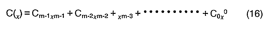
- Next, C(χ) is divided by the generator polynomial G(χ). Here, the explanation will be made of the case of division by the generator polynomial of g+1 bits as the generator polynomial G(x). If G(χ)=χ8+χ2+χ+1, g = 8 (8-th order), but here the explanation will be made of the general method in the case of finding the CRC arithmetic operation result (remainder) R(x) by performing the CRC arithmetic operation (division) by the generator polynomial of g+1(=9) bits.
- The operation result R(x) at this time is expressed by:
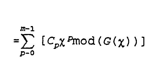
modulo 2 operation. Further, p is the order of the input bit train Bin, for example, p=0 to p=39 (in case of input bit train Bin of 40 bits). - Here, to further develop the equation, a code train Eρ(χ) with a special value is introduced:

- If the Eρ(χ) is inserted in the above equation (17), then the following is obtained:

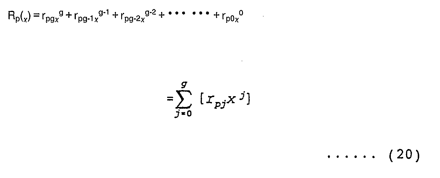
- Note that g in equation (20) is the above-mentioned g.
- Therefore, if equation (20) and equation (17) are inserted in equation (19), the following equation (21) is obtained:


- The point to be noted here is the conversion from equation (21) to equation (22). This is based on the known conversion rule that the value does not change even if the order of E is switched. The coefficient rj of the term of the j-th order of the remainder R(x) found by this equation (22) may be found by calculating the equation (23):

- Therefore, the number of the terms where the coefficient of the term of the p-th order (0 to 39) of the received code C(χ) is "1", that is, the term of
- When incorporating a
wired logic unit 51 of Fig. 20 based on the above-mentioned mathematical method, the remainder R(χ) obtained by dividing each of the above-mentioned Ep(χ) by the generator polynomial G(χ) is decided readily in advance, so by using this it is possible to make the wiredlogic unit 51 and theremainder arithmetic unit 52 extremely simple in construction and reduce the size of the hardware required. - Figure 21 is a view of an example of realization of the third embodiment. In the figure, the wired
logic unit 51 is made of the wiring illustrated. The input side is connected to an m-bit shift register 21 (in the figure, m=0 to m=39), each bit part being comprised of a flipflop FF. Coo, C01 ··· C39 correspond to the above-mentioned C(x). The output side of the wiredlogic unit 51 enters theinput gates 53 of theremainder arithmetic unit 52. Theinput gates 53 are, for example, comprised of known parity check circuits (PC). The bits (χ7,χ6··· x°) output from the parity check circuits PC (for example, comprised of EX-OR gate group) become the CRC arithmetic operation results Cout (corresponding to the above-mentioned R(x)) sought. In the same way as the above-mentioned embodiment, this Cout is input to thesynchronization control unit 23. - Since the CRC arithmetic operation results for a monomial can be found in advance by calculation, the wired
logic unit 51 of Fig. 21 has its internal wiring determined by the calculation results. That is, as mentioned above, the remainder R(x) obtained by dividing the above-mentioned Eρ(χ)'s one by one by the generator polynomial G(χ) is determined readily in advance, so this is used. - Figure 22 is a view of the bit pattern for constituting the wired logic unit of Fig. 21. In the bit pattern diagram, the monomials Ep(x) are bit trains with just one of the 40 bits being "1" and the remainder all being "0", with the "1 bit differing in bit position. In the figure, the "1" bits are arranged in a line slanting from the top left to the bottom right. The remainders R(χ)'s obtained by dividing the values of the Eρ(χ)'s corresponding to x 39, x 38·· χ 00 by the generator polynomial G(χ) become the 8-bit bit trains shown in the right column of the figure. For example, for the term of x 39, the remainder becomes: 00110001
- For the term of χ 39 , the wiring is performed on the
input gates 53 corresponding to the bit positions (3) of the "1" bits among the above-mentioned eight bits (00110001). In Fig. 14, it will be understood, wiring is performed for and χ0 for C39 (illustration omitted for χ 4). Further, for example, for the term of χ 38, the remainder becomes: 10011011 - For the term of χ 38, the wiring is performed on the
input gates 53 corresponding to the bit positions (5) of the "1 " bits among the above-mentioned eight bits (10011011). In Fig. 14, it will be understood, wiring is performed for χ 7 and χ 0 for C38 (illustration omitted for χ 1, χ 3, and χ 4). - The horizontally extending wiring group and the parity check circuits (PC) receiving the same in the wired
logic unit 51 in Fig. 21 are used to perform an operation equivalent to the addition of the bit trains in the right column of Fig. 22 in the lateral direction with the bit positions (j bits) matched and to obtain the desired remainder R(χ). - Figure 23 is a view of a fourth embodiment according to the present invention. In the figure, the continuous CRC
arithmetic unit 22 is made of a remainderarithmetic unit 61 and adelay unit 62. Further, theshift register unit 21 is comprised of a k-stage shift register. k is a specific number which is larger than 1 and smaller than the number of bits (for example, 8) making up one octet of the ATM cell. The bit output of the first stage of the k-stage shift register and the bit output of the k-th stage form two of the three inputs used for the CRC arithmetic operation in theremainder arithmetic unit 61. The remaining one input is the output from thedelay unit 62. From theremainder arithmetic unit 61 is output the CRC arithmetic operation results Cout successively and continuously in accordance with the shift timing. This Cout is on the one hand output to thesynchronization control unit 23 in the same way as the previously mentioned embodiment and on the other hand is output to thedelay unit 62. Therefore, what is given from thedelay unit 62 to the input of theremainder arithmetic unit 61 is the CRC arithmetic operation result obtained just before. - Therefore, the
remainder arithmetic unit 61 executes the predetermined operation receiving these three inputs and produces the CRC arithmetic operation results Cout. - The fourth embodiment is established taking note of a certain mathematical method which will be explained below. First, see Fig. 24.
- Figure 24 is a view of the general format of the ATM cell used for explaining the fourth embodiment. The figure shows the ATM cell shown in Fig. 9 with the header data in bit units. The following explanation will be made in terms of these bit units.
- If the time series in the input bit train Bin is taken out and made W, then it may be expressed as:

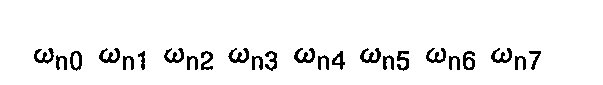

- Here, in the above-mentioned time series W, when five octets corresponding to the header of the ATM cell, that is, ωn + ωn+4 are taken out, the CRC arithmetic operation results Cout are made Cn. Further, the generator polynomial used for the CRC arithmetic operation is made G. Then, the CRC calculation results Cn are expressed by


- In equation (26), ωnx 8x4 corresponds to the first octet, ωn+1χ 8x3 corresponds to the second octet, ·· and ωn+4χ 8x0 corresponds to the fifth octet.
- Here, if a mathematical inductive method is used and consideration given to the Cn+1 appearing at the timing following Cn, then Cn + can be expressed as follows:
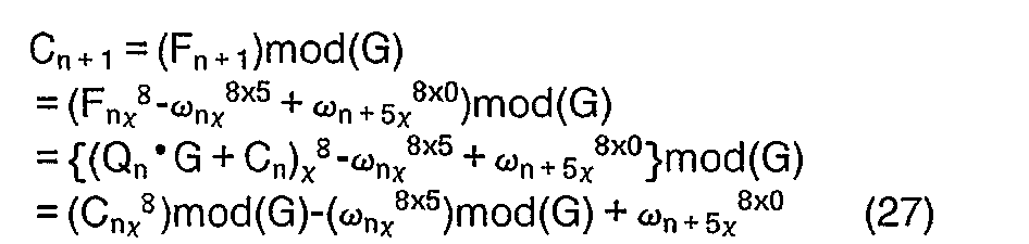
- Here, the following six initial conditions are set for the equation (27):

- If the above initial conditions are set in the equation (27), the CRC arithmetic operation results Cn sought are expressed by the following equation:

- As clear from the final conclusion, that is, the above equation (28), the CRC arithmetic operation results Cn sought can be expressed extremely simply using the three elements Cn.i, ωn-1, and ωn+4. These three elements, however, are coefficients of X 8, χ 8x5, and χ 8x0 and occur at different times from each other, so when the
remainder arithmetic unit 61 executes the arithmetic operations on the three elements, the three elements must be obtained at the same timing at the input of theremainder arithmetic unit 61. The k-stage shift register 21 anddelay unit 62 shown in Fig. 23 exist for matching the above timings. Note that the three elements Cn-1, ωn-1, and ωn+4 shown in the above-mentioned equation (28) appear at the portions shown in Fig. 23. - Figure 25 is a view of an example of realization of the fourth embodiment. In the figure, the k-
stage shift register 21 is comprised of a 6-stage shift register (comprised of six flipflops FF connected in tandem). The above-mentioned element ωn-1 is supplied from the first stage output receiving the input bit train Bin, while the above-mentioned element ωn+4 is supplied from the sixth stage output. These are applied to theremainder arithmetic unit 61. The other element Cn-1 to be input to theremainder arithmetic unit 61 is given from thedelay unit 62. This may be comprised of a D-flipflop DFF as illustrated. The clock CLK defining the overall timing is, for example, a speed of 4M. The bit outputs Do, D1 ··· D5 are sent out from these FF's in synchronization with this. Further, the reset signal RST is given to the reset inputs of the FF's. The reset signal RST rises at the same time as the reception of the input bit train Bin (see Fig. 26) and falls when the reception of Bin is completed. - Figure 26 is a timing chart of signals appearing at key portions of Fig. 25. In the figure, the same references (CLK, Bin···) are given to the rows corresponding to the signals of Fig. 25. The downward facing arrow Bin in the row of Do shows that the above-mentioned three elements (ωn-1, (ωn+4, Cn-1) are matched at the same time as ω5, ω0, and Co for the first time since being input. The CRC arithmetic operation results sought are C1.
- Next, a detailed explanation will be given of the
remainder arithmetic unit 61 in Fig. 25. - Figure 27 is a view of a detailed example of a remainder arithmetic unit. In the figure, the
remainder arithmetic unit 61 is comprised, for example, of the illustratedwired logic unit 63, theEX-OR gate 64, and 8-bit leading wires 65 for output of the CRC arithmetic operation results. The wiredlogic unit 63 receives at the input side the above-mentioned three elements ωn+4, ωn-1, and Cn-1 as the bit outputs D5 and Do of the 6-stage shift register 21 and the output of thedelay unit 62 and is connected at the output side to eight EX-OR gates 64 (only three shown) corresponding to the eight bits. The wiredlogic unit 63 is assembled as shown in Fig. 27 for a similar reason as to why the wiredlogic unit 51 is assembled as shown in Fig. 21 in the above-mentioned third embodiment. That is, the CRC arithmetic operation results for the inputs Dε and Do and Cn-1 in Fig. 27 can be calculated in advance (see row R(X) in Fig. 22), so this is used for wiring the wiredlogic unit 61. - Figure 28 is a view of the bit pattern for constituting the portion corresponding to the bit output Do in the wired logic unit of Fig. 27, Fig. 29 is a view of the bit pattern for constituting the portion corresponding to the bit output D5 in the wired logic unit of Fig. 27; and Fig. 30 is a view of the bit pattern for constituting the portion corresponding to the immediately preceding CRC arithmetic operation result Cn-1 in the wired logic unit of Fig. 27.
- Regarding Do of Fig. 28, for example, the line connection corresponding to the "1" bit in the bit train of the order χ7 becomes the connection point A of the Do row in Fig. 27. Further, for Ds of Fig. 29, for example, the line connection corresponding to the "1" bit in the bit train of the order χ 41 (only the two consecutive bits on the left side shown) becomes the connection point B of the Dε row of Fig. 27. Further, for Cn-1 of Fig. 30, for example, the line connection corresponding to the "1" bit in the bit train of the order χ 14 (only the two consecutive bits of the left side and the one bit of the right side shown) becomes the connection point C of the row Cn-1 of Fig. 27. After this line connection, connection is made to the corresponding inputs of the
EX-OR gate 64 made into bundles of eight corresponding to the 8 bits of the Cn. The EX-OR gate performs an addition function and the results of the addition are sent out as Cn to the leadingwires 65 corresponding to the bits. - When the synchronization circuit (20 in Fig. 8) is actually used in an ATM communication system, the synchronization circuit provided at the side receiving the ATM cells must function to provide rear protection and front protection as well. That is, the synchronization control unit (23 in Fig. 8) must include a rear protection and front protection means. Usually, rear protection is provided seven times and front protection six times.
- Even if cell synchronization is detected for the first time by the above-mentioned CRC arithmetic operation from the header of the ATM cells begun to be received, it is not known if that true cell synchronization is detected. Therefore, if similar cell synchronization is detected continuously seven times, it is deemed that true cell synchronization has been detected and the synchronization detection signal (Sd in Fig. 8) is started to be supplied. This is what is meant by seven times of rear protection.
- Once cell synchronization has been established, cell synchronization is continued to be detected during the usual reception of data, but the synchronization detection signal Sd is not always normally received. Cases when the Sd is not received include cases where the cell synchronization is lost and Sd is not obtained and cases where the synchronization detection signal should be obtained, but noise or the like causes the synchronization detection signal to be not received in actuality. In the former case, the reception of data is immediately suspended and cell synchronization must be detected again. In the latter case, however, there is no need for this. This is because the data can continue to be normally received under these conditions. Therefore, once cell synchronization has been established, it is deemed that cell synchronization has really been lost only when cell synchronization cannot be detected six successive times, in which case the supply of the synchronization detection signal Sd is stopped. This is what is meant by six times of front protection. Therefore, the
synchronization circuit 20 of the present invention is preferably provided with a rear protection and front protection function. - Figure 31 is a block diagram of the principle of a synchronization circuit including a reset means. The
synchronization circuit 20 in the figure is provided with a reset means 70 at thesynchronization control unit 23 at the reception side. The reset signal R/S from the reset means 70 is applied to theshift register unit 21 and the continuous CRCarithmetic unit 22. - According to the CCITT recommendations, once cell synchronization has been established, it is possible to predict the timing at which the next synchronization detection is possible, so during that period the synchronization detection operation may be suspended. In accordance with this, the rear protection function and the front protection function can be started up at cycles of 53 bytes (53 octets). In this case, the synchronization circuit of the present invention would not function with just the synchronization detection started up every 53 bytes. This is because the
synchronization circuit 20 has theshift register unit 21 with the data holding function and the CRC arithmetic unit 22 (CRC memory unit 36 and delay unit 62). That is, it is necessary to reset the past data remaining in the data holding function unit. Therefore, the reset means 70 is provided. This reset means 70 is essential for performing the rear protection and front protection. A detailed example will be provided below: - Figure 32 is a view of an example of application of the reset means to the synchronization circuit of Fig. 14. The operation in the figure is as follows: Here, the
ROM 35 has written in it the results of calculation of the Cn + from an, an+40, and Cn in advance. - i) When n = -39 (initial state)
- The
synchronization control unit 23 sends the reset signal R to the CRCarithmetic processing unit 71. This resets the internal states of theshift register 21 and theCRC memory unit 36 in the CRCarithmetic processing unit 71.
- The
- ii) When n = -38
- The initial data a1 is input in the LSB of the
shift register 21 and theROM 35. At this time, at theshift register 21, the data is shifted in the direction from the LSB to the MSB (right direction in the figure). Further, at this time, simultaneously the CRC arithmetic operation result of the state just before (initial state), that is, the all "0" state, from theCRC memory unit 36 and, further, the "0" from the MSB of the shift register are input. In this state, the next CRC arithmetic operation result is read from theROM 35 and is set in theCRC memory unit 36. - At this time, data of the number of bits sufficient for performing the desired CRC arithmetic operation is not input to the CRC
arithmetic processing unit 71, so thesynchronization control unit 23 does nothing.
- The initial data a1 is input in the LSB of the
- iii) when -37sns_0
- The data an+39 is input to the LSB of the
shift register 21 and theROM 35. At this time, in the shift register, the data is shifted in the direction from the LSB to the MSB (right direction in the figure). Further, at this time, simultaneously the CRC arithmetic operation result of the state just before (initial state) from theCRC memory unit 36 and, further, the "0" from the MSB of the shift register are input. In this state, the next CRC arithmetic operation result is read from theROM 35 and is set in theCRC memory unit 36. - At this time, data of the number of bits sufficient for performing the desired CRC arithmetic operation is not input to the CRC
arithmetic processing unit 71, so thesynchronization control unit 23 does nothing.
- The data an+39 is input to the LSB of the
- iv) When n = 1
- The data aq.o is input to the LSB of the
shift register 21 and theROM 35. At this time, in the shift register, the data is shifted in the direction from the LSB to the MSB (right direction in the figure). Further, at this time, simultaneously the CRC arithmetic operation result of the state just before (initial state) from theCRC memory unit 36 and, further, the "0" from the MSB of the shift register are input. In this state, the next CRC arithmetic operation result is read from theROM 35 and is set in theCRC memory unit 36. - Data of the number of bits sufficient for performing the desired CRC arithmetic operation is input to the CRC
arithmetic processing unit 71, so thesynchronization control unit 23 waits until the desired CRC arithmetic operation results become synchronized.
- The data aq.o is input to the LSB of the
- v) When n>__2
- The data a,.39 is input to the LSB of the
shift register 21 and theROM 35. At this time, in the shift register, the data is shifted in the direction from the LSB to the MSB (right direction in the figure). Further, at this time, simultaneously the CRC arithmetic operation result of the state just before (initial state) from theCRC memory unit 36 and, further, the an-1, from the MSB of the shift register are input. In this state, the next CRC arithmetic operation result is read from theROM 35 and is set in theCRC memory unit 36. - Data of the number of bits sufficient for performing the desired CRC arithmetic operation is input to the CRC
arithmetic processing unit 71, so thesynchronization control unit 23 waits until the desired CRC arithmetic operation results become synchronized.
- The data a,.39 is input to the LSB of the
- In the state after vi) and iv), the synchronization detection signal Sd is output from the
synchronization control unit 23 in the state where the conditions for front protection for synchronization have been met. - In the state after vii) and vi), when the desired CRC arithmetic operation results are not synchronized at the desired position, the set signal is output from the
synchronization control unit 23. The CRC arithmetic processing unit is set to a state waiting for the same meaning as the internal state desired in the synchronization state (shift register - all "0", CRC memory unit - all "0"). - In the state of viii) and vi), when loss of synchronization is detected, a reset signal is output from the
synchronization control unit 23, the synchronization detection signal disappears, and the state i) is returned to. - Figure 33 is a view of an example of a
synchronization control unit 23 in Fig. 32. This includes a reset means 70. - Figure 34 is a timing chart showing the reset signal in Fig. 33. 424 in the figure means 53 (all octets in ATM cell) x 8 (bits) and 40 means 5 (all octets of header in ATM cell) x 8 (bits). The reset signal R/S is output cyclically as illustrated and is output to the CRC arithmetic processing unit 71 (Fig. 32).
- The
hunt processing unit 72 is in a hunting state. - When the reset of the master is released, the CRC
arithmetic processing unit 71 starts the CRC arithmetic operation and Cn's are successively input to thecomparator unit 24. - In the
comparator unit 24, when Cn matches the desired value, the coincidence signal is output. At this time, the signal PS showing that the pseudo synchronization has started is output from thehunt processing unit 72, and the rear protection operation is started at the rear protection unit 73. - The rear protection unit 73 which starts the rear protection operation checks that the coincidence signal is received successively seven times for each 53 bytes from the point of time when the signal PS is input. At this time, the synchronization start signal SS is output to the
front protection unit 74. - When seven successive coincidence signals cannot be received, the reset signals R2 and R/S are sent to the
hunt processing unit 72 and the CRCarithmetic processing unit 71 and the above-mentioned state (2) is returned to. - Continuing after the above-mentioned state (3), the synchronization state exists while the coincidence signal is input to the
front protection unit 74 every 53 bytes. - When the coincidence signal coming every 53 bytes stops, the
front protection unit 74 enters the front protection state. At this time, just the synchronization detection signal Sd is output every 53 bytes. When the coincidence signal is not input for six successive times, thefront protection unit 74 outputs the reset signals R1 and R/S and the above-mentioned state (1) is returned to. When the coincidence signal is once again input in the 53 x i (i<6) byte, the above-mentioned state (4) is returned to. - Figure 35 is a view of an example of incorporation of the reset means in the circuit of Fig. 25.
- The reset means 70, in brief, executes the CRC arithmetic operation on the 5 octets from the header every 53 octets (length of one ATM cell) and is essential for the rear protection and front protection. A detailed example was given in Fig. 32.
- The second detailed example shown in Fig. 35 has a reset means 70 built in the synchronization circuit of Fig. 25. The reset means 70 can be extremely easily realized by an AND
gate 75. This is also an advantage of the synchronization circuit of Fig. 25. - The AND
gate 75 receives as input the above-mentioned reset signal RST and the output H of a header counter (not shown) and outputs the reset signal R/S. The reset signal R/S is applied to the sixth stage flipflop FF and the reset inputs of the flipflop forming thedelay unit 62. Note that the above-mentioned header counter produces a cyclic output H synchronized with 53 octets.The waveform is shown in the row H of Fig. 36. - Figure 36 is a timing chart of signals appearing at key portions of Fig. 35.
- As mentioned in the beginning, the CRC arithmetic operation is used not only for the detection of cell synchronization, but also for correcting errors in the header itself of the ATM cells. Therefore, the
synchronization control unit 23 in thesynchronization circuit 20 is provided with a header error correction means in addition to the above-mentioned reset means 70. Below, an example of a header error correction means suitable for being incorporated in thesynchronization control unit 23 is shown. - As mentioned above, the header error correction means enters the active state after the synchronization circuit enters the synchronization state through the above-mentioned rear protection. Strictly speaking, this is the synchronization state when there is no error in the header of the ATM cell appearing just before. Therefore, consider the definite time series ψ:
- ψo ψ1 02 ψ3 ψ4
- where oi is
- ψi0ψi1 ψi2ψi3ψi4ψi5ψi6ψi7
- Expressing this by a polynomial, the
time series 0 is a numerical equation expressed by:
- Here, it is considered that the CRC arithmetic operation results C aimed at are C = 0. That is,

- However, assume that a one-bit error E enters the time series ψ. In this case, E is expressed by


bits 0 to 7, then
- On the other hand, analyzing the generator polynomial G, the general generator polynomial G (=χ 8 +χ 2+χ+1 becomes


- In equation (36), if the value i which gives 0≦(i + e)mod(127)≦7 is selected, the syndrome S' can be simply found. That is,

- Here, as a result, it is known that


- Next, the following are found:

- S in equation (40) shows the initial state of the data and may be illustrated as follows:Note that [1] to [5] correspond to the first octet to fifth octet of the header of the ATM cell. Further, the code length is 127 bits.

- The above-mentioned equation (41) means that the 87 bits of the header in the S: of the above figure are moved to the right in the bit train. As a result, the header is cyclically replaced to the higher order side as shown by the following S-i:

- Next, if the first octet [1] of the header is moved to the right, the following So is obtained. This So has the i in the above equation (42) made i = 0.


- Below, similarly if another octet is moved to the right, S1, becomes


- Therefore, finally the following results:
- a) When S = 0 (or S-1 = 0) -> no error.
- b) When S; = χ j (0≦j≦7) -> the processing of (ωi(7-j)<-1 +ωi(7-j) becomes necessary (bit inversion).
- c) When (0≦j≦4) and the condition in the previous two terms are not met -> cell disposal is indicated.
- Here, one of the error correction information a), b), and c) are obtained.
- An example of the specific constitution of the header error correction means based on the above will be explained below:
- Figure 37 is a view of a specific example of a header error correction means. However, this is an example of application to the synchronization circuit shown in Fig. 35. Further, Fig. 38 is a timing chart of signals appearing at key portions of Fig. 37. The example will be explained referring to these figures. First, in Fig. 37, the portion other than the
bit correction unit 89 is the bit error detection unit. The bit error detection unit is comprised of the illustratedcircuit elements 82 to 88. Theflipflops bit correction unit 89. Further, the S-i,arithmetic unit 84 and the Siarithmetic unit 87 execute the bit shift mentioned above. - Figure 39 is a view of an example of the S-1 arithmetic unit in Fig. 37. Figure 40 is a view of the bit pattern for constituting the S-1 arithmetic unit of Fig. 39. Figure 41 is a view of one example of the S1 arithmetic unit in Fig. 37. Figure 42 is a view of the bit pattern for constituting the S; arithmetic unit in Fig. 41.
- Next, an explanation will be made of the
bit correction unit 89 of Fig. 37. - Figure 43 is a view of an example of the bit correction unit of Fig. 37. Figure 44 is a timing chart of signals appearing at key portions of Fig. 43.
- In Fig. 43, 91 is an arithmetic circuit, 92 to 94 are flipflops, and 95 is an EX-OR gate. A header error is detected at the stage in front of the
block 89 in Fig. 37. After this, the error is corrected by thebit correction unit 89 of Fig. 43 by the operation of Fig. 44. In the header error correction here, by obtaining the EX-OR E of the data when Si has a one-bit error and ωi by theEX-OR gate 95, the corrected data bit T is obtained. Here, first, consideration will be given to thearithmetic circuit 91. - The
arithmetic circuit 91 - (i) outputs "1 when Si = 0 or when Si has a one-bit error and
- (ii) outputs "0" when Si has two or more bits of error.
- The construction of the
arithmetic circuit 91 will be discussed later, but here note that the corrected data bit T is obtained by resetting the D-flipflop 92 by the output Rc of thecircuit 91. This is because the EX-OR can be obtained only when Si = 0 or Si has a one-bit error. - On the other hand, looking at the
RS flipflop 93, the Q output U - i) becomes "1 when S; = 0 or Si has a one-bit error and
- ii) becomes "0" when Si has two or more bits of error.
- The above-mentioned
arithmetic circuit 91 will be explained in further detail below. Here, assume that the Si mentioned above is expressed by Si: S10 S11 S12 S13 S14 S15 S16 S17 - i) When Si =0

arithmetic circuit 91. - ii) When
S i has a one-bit error
arithmetic circuit 91. - Other than the above, there are two or more bits of error.
- In the final analysis, the output Rc of the
arithmetic circuit 91 becomes the logical OR output of the above-mentioned Rca and Rcb. - The ATM cells are continuously sent in from the transmission side on the transmission channel. If this transmission channel is disconnected, the all "0" or all "1" data appears at the reception side. If the all "0" data appears, the CRC arithmetic operation result also becomes "0" and the reception side enters a state equivalent to one where synchronization is established. This is the pseudo synchronization detection state.
- Therefore, it has been proposed at the CCITT that an offset bit train be mapped at the HEC region (HEC in Fig. 9) in the header of the ATM cells at the transmission side in advance. This offset bit train would, for example, be as follows:
- 01010101
- To deal with the case of mapping of such an offset bit train, a logic inversion means is introduced in the present invention.
- Figure 45 is a block diagram of the principle of a synchronization circuit including a logic inversion means.
Reference numeral 100 in the figure is a logic inversion means. For "1", the bit corresponding to the CRC arithmetic operation result is inverted in logic. On the other hand, for "0", the bit corresponding to the CRC arithmetic operation result is passed with its logic as is. Showing this operation by a numerical equation, looking at the above-mentioned equation (17),
- Figure 46 is a view of an example of a logic inversion means. The logic inversion means 100 is applied to the continuous CRC
arithmetic unit 22 of Fig. 21 (third embodiment). The logic inversion means of Fig. 45 is comprised of a group ofinvertors 101. Theinvertor 101 is connected at the bit position corresponding to "1 " in the above-mentioned offset bit train. - As explained above, according to the present invention, it is possible to perform a CRC arithmetic operation continuously on the header portion of bit trains of continuously input ATM cells and to detect synchronization at a high speed. Further, the hardware for this can be extremely simply realized based on a mathematical method.
Therefore, when Si includes two or more bits of error, U4 still shows "0". At this time, the ATM cell is discarded. Note that the RS flipflop 93 is set by S1 showing the header of the ATM cell.
Claims (21)
Applications Claiming Priority (2)
| Application Number | Priority Date | Filing Date | Title |
|---|---|---|---|
| JP6804990 | 1990-03-20 | ||
| JP68049/90 | 1990-03-20 |
Publications (3)
| Publication Number | Publication Date |
|---|---|
| EP0448074A2 true EP0448074A2 (en) | 1991-09-25 |
| EP0448074A3 EP0448074A3 (en) | 1993-01-27 |
| EP0448074B1 EP0448074B1 (en) | 1998-06-10 |
Family
ID=13362543
Family Applications (1)
| Application Number | Title | Priority Date | Filing Date |
|---|---|---|---|
| EP91104331A Expired - Lifetime EP0448074B1 (en) | 1990-03-20 | 1991-03-20 | Synchronization circuit for ATM cells |
Country Status (5)
| Country | Link |
|---|---|
| US (1) | US5282215A (en) |
| EP (1) | EP0448074B1 (en) |
| JP (1) | JPH04211547A (en) |
| CA (1) | CA2038592C (en) |
| DE (1) | DE69129558T2 (en) |
Cited By (8)
| Publication number | Priority date | Publication date | Assignee | Title |
|---|---|---|---|---|
| WO1995018495A1 (en) * | 1993-12-27 | 1995-07-06 | Koninklijke Ptt Nederland N.V. | Device for establishing cell boundaries in a bit stream and crc calculation |
| EP0750400A1 (en) * | 1995-06-22 | 1996-12-27 | STMicroelectronics S.A. | Syndrome computing circuit |
| EP0682790A4 (en) * | 1993-11-22 | 1998-05-20 | Motorola Inc | Method and system for synchronizing encoders and decoders in communication networks when errors are detected. |
| GB2323503A (en) * | 1997-03-05 | 1998-09-23 | Nec Corp | ATM cell synchronisation circuit |
| US5845239A (en) * | 1993-07-30 | 1998-12-01 | Texas Instruments Incorporated | Modular audio data processing architecture |
| EP0838969A3 (en) * | 1996-10-24 | 1999-03-24 | AT&T Corp. | Fast framing of the ATM protocol used alone by header error check |
| EP0898395A3 (en) * | 1997-08-21 | 2004-01-07 | Nokia Corporation | Method and system for locating datapackets in a serial data stream |
| WO2009064599A1 (en) * | 2007-11-12 | 2009-05-22 | Motorola, Inc. | Continuous redundancy check method and apparatus |
Families Citing this family (35)
| Publication number | Priority date | Publication date | Assignee | Title |
|---|---|---|---|---|
| US5375127A (en) * | 1992-03-25 | 1994-12-20 | Ncr Corporation | Method and apparatus for generating Reed-Soloman error correcting code across multiple word boundaries |
| GB9213273D0 (en) * | 1992-06-23 | 1992-08-05 | Digital Equipment Int | Efficient atm cell synchronization |
| KR950009690B1 (en) * | 1993-09-14 | 1995-08-26 | 재단법인한국전자통신연구소 | Crc synchronizing apparatus |
| KR970004256B1 (en) * | 1994-06-29 | 1997-03-26 | 한국전기통신공사 | Frame / Burst Synchronization and Error Detection System Using Cyclic Code |
| US5771249A (en) * | 1994-09-02 | 1998-06-23 | Toyo Communication Equipment Co., Ltd. | ATM cell synchronous system |
| US5600653A (en) * | 1994-09-30 | 1997-02-04 | Comsat Corporation | Technique for improving asynchronous transfer mode operation over a communications link with bursty bit errors |
| US5703887A (en) * | 1994-12-23 | 1997-12-30 | General Instrument Corporation Of Delaware | Synchronization and error detection in a packetized data stream |
| JP3454962B2 (en) * | 1995-03-23 | 2003-10-06 | 株式会社東芝 | Error correction code encoder and decoder |
| US5623483A (en) * | 1995-05-11 | 1997-04-22 | Lucent Technologies Inc. | Synchronization system for networked multimedia streams |
| US5602767A (en) * | 1995-08-29 | 1997-02-11 | Tcsi Corporation | Galois field polynomial multiply/divide circuit and a digital signal processor incorporating same |
| US5774480A (en) * | 1995-10-10 | 1998-06-30 | Allied Telesyn International Corporation | Cyclic code check bits generation and error correction using sum of remainders |
| JPH09116541A (en) * | 1995-10-16 | 1997-05-02 | Toshiba Corp | Communication control device |
| US6061741A (en) * | 1997-05-28 | 2000-05-09 | International Business Machines Corporation | Method and apparatus for synchronization of connectionless applications across a network by using simple encryption tokens |
| US5951707A (en) * | 1997-06-27 | 1999-09-14 | International Business Machines Corporation | Method of partitioning CRC calculation for a low-cost ATM adapter |
| US6295626B1 (en) * | 1997-10-20 | 2001-09-25 | Nortel Networks Limited | Symbol based algorithm for hardware implementation of cyclic redundancy check |
| US6681364B1 (en) | 1999-09-24 | 2004-01-20 | International Business Machines Corporation | Cyclic redundancy check for partitioned frames |
| US6587988B1 (en) * | 1999-12-22 | 2003-07-01 | Intel Corporation | Dynamic parity inversion for I/O interconnects |
| JP4515651B2 (en) * | 2001-03-05 | 2010-08-04 | ルネサスエレクトロニクス株式会社 | Cyclic redundancy check operation method and cyclic redundancy check operation circuit |
| US20020144208A1 (en) * | 2001-03-30 | 2002-10-03 | International Business Machines Corporation | Systems and methods for enabling computation of CRC' s N-bit at a time |
| TW503636B (en) * | 2001-04-12 | 2002-09-21 | Realtek Semiconductor Corp | HEC checking method and circuit for sequential feed back type cell of asynchronous transfer mode |
| US6928608B2 (en) * | 2001-08-14 | 2005-08-09 | Optix Networks Ltd. | Apparatus and method for accelerating cyclic redundancy check calculations |
| JP2003078421A (en) * | 2001-09-04 | 2003-03-14 | Canon Inc | Code sequence head position detection method and apparatus, decoding method using the same, and apparatus therefor |
| US7047479B1 (en) * | 2002-02-04 | 2006-05-16 | Cypress Semiconductor Corp. | Parallel CRC formulation |
| US7458006B2 (en) * | 2002-02-22 | 2008-11-25 | Avago Technologies General Ip (Singapore) Pte. Ltd. | Methods for computing the CRC of a message from the incremental CRCs of composite sub-messages |
| US7178084B2 (en) * | 2002-09-25 | 2007-02-13 | Infineon Technologies Ag | Short error propagation modulation coding method and device |
| US20040098655A1 (en) * | 2002-11-19 | 2004-05-20 | Sharma Debendra Das | Rolling CRC scheme for improved error detection |
| US20090024900A1 (en) * | 2007-07-18 | 2009-01-22 | Cisco Technology, Inc. | Cyclic redundancy checking in lane-based communications |
| EP2026470A1 (en) * | 2007-08-17 | 2009-02-18 | Panasonic Corporation | Running cyclic redundancy check over coding segments |
| JP4798164B2 (en) * | 2008-04-02 | 2011-10-19 | ソニー株式会社 | Transmitting apparatus and method, receiving apparatus and method, and program |
| US8402342B2 (en) | 2010-02-26 | 2013-03-19 | Research In Motion Limited | Method and system for cyclic redundancy check |
| US8433004B2 (en) * | 2010-02-26 | 2013-04-30 | Research In Motion Limited | Low-latency viterbi survivor memory architecture and method using register exchange, trace-back, and trace-forward |
| KR20120095221A (en) * | 2011-02-18 | 2012-08-28 | 삼성전자주식회사 | Memory device and memory control unit |
| JP5982869B2 (en) * | 2012-02-28 | 2016-08-31 | 富士ゼロックス株式会社 | Transmission / reception system and program |
| US9960788B2 (en) * | 2015-03-27 | 2018-05-01 | Toshiba Memory Corporation | Memory controller, semiconductor memory device, and control method for semiconductor memory device |
| US11949510B2 (en) * | 2022-09-06 | 2024-04-02 | Qualcomm Incorporated | Hardware-based dynamic cyclic-redundancy check (CRC) generator for automotive application |
Family Cites Families (6)
| Publication number | Priority date | Publication date | Assignee | Title |
|---|---|---|---|---|
| BE656364A (en) * | 1963-11-29 | |||
| US4498174A (en) * | 1982-08-25 | 1985-02-05 | Ael Microtel Limited | Parallel cyclic redundancy checking circuit |
| US4593393A (en) * | 1984-02-06 | 1986-06-03 | Motorola, Inc. | Quasi parallel cyclic redundancy checker |
| DE3707143A1 (en) * | 1987-03-06 | 1988-09-15 | Blaupunkt Werke Gmbh | DEVICE FOR RECEIVING DATA |
| JPH03505035A (en) * | 1989-02-16 | 1991-10-31 | グラマン エアロスペース コーポレーション | Ultra-fast error detection network |
| US5103451A (en) * | 1990-01-29 | 1992-04-07 | Motorola, Inc. | Parallel cyclic redundancy check circuit |
-
1991
- 1991-02-28 JP JP3034196A patent/JPH04211547A/en active Pending
- 1991-03-19 CA CA002038592A patent/CA2038592C/en not_active Expired - Fee Related
- 1991-03-20 EP EP91104331A patent/EP0448074B1/en not_active Expired - Lifetime
- 1991-03-20 US US07/672,863 patent/US5282215A/en not_active Expired - Lifetime
- 1991-03-20 DE DE69129558T patent/DE69129558T2/en not_active Expired - Fee Related
Cited By (13)
| Publication number | Priority date | Publication date | Assignee | Title |
|---|---|---|---|---|
| US5845239A (en) * | 1993-07-30 | 1998-12-01 | Texas Instruments Incorporated | Modular audio data processing architecture |
| EP0682790A4 (en) * | 1993-11-22 | 1998-05-20 | Motorola Inc | Method and system for synchronizing encoders and decoders in communication networks when errors are detected. |
| NL9302266A (en) * | 1993-12-27 | 1995-07-17 | Nederland Ptt | Device for determining limits in a bitstream, and converting means for use in the device. |
| AU683712B2 (en) * | 1993-12-27 | 1997-11-20 | Koninklijke Kpn N.V. | Device for establishing cell boundaries in a bit stream and CRC calculation |
| WO1995018495A1 (en) * | 1993-12-27 | 1995-07-06 | Koninklijke Ptt Nederland N.V. | Device for establishing cell boundaries in a bit stream and crc calculation |
| EP0750400A1 (en) * | 1995-06-22 | 1996-12-27 | STMicroelectronics S.A. | Syndrome computing circuit |
| FR2735889A1 (en) * | 1995-06-22 | 1996-12-27 | Sgs Thomson Microelectronics | SYNDROME CALCULATION CIRCUIT |
| EP0838969A3 (en) * | 1996-10-24 | 1999-03-24 | AT&T Corp. | Fast framing of the ATM protocol used alone by header error check |
| GB2323503B (en) * | 1997-03-05 | 1999-02-10 | Nec Corp | ATM cell synchronization circuit |
| GB2323503A (en) * | 1997-03-05 | 1998-09-23 | Nec Corp | ATM cell synchronisation circuit |
| EP0898395A3 (en) * | 1997-08-21 | 2004-01-07 | Nokia Corporation | Method and system for locating datapackets in a serial data stream |
| WO2009064599A1 (en) * | 2007-11-12 | 2009-05-22 | Motorola, Inc. | Continuous redundancy check method and apparatus |
| US8261154B2 (en) | 2007-11-12 | 2012-09-04 | Motorola Mobility Llc | Continuous redundancy check method and apparatus |
Also Published As
| Publication number | Publication date |
|---|---|
| EP0448074B1 (en) | 1998-06-10 |
| CA2038592A1 (en) | 1991-09-21 |
| DE69129558D1 (en) | 1998-07-16 |
| DE69129558T2 (en) | 1998-12-10 |
| JPH04211547A (en) | 1992-08-03 |
| CA2038592C (en) | 1995-11-21 |
| US5282215A (en) | 1994-01-25 |
| EP0448074A3 (en) | 1993-01-27 |
Similar Documents
| Publication | Publication Date | Title |
|---|---|---|
| EP0448074A2 (en) | Synchronization circuit for ATM cells | |
| US5345451A (en) | Cyclic redundancy check operating method and a head error checker synchronizing unit in an asynchronous transfer mode switching process | |
| US5577037A (en) | Method of processing inclusively STM signals and ATM signals and switching system employing the same | |
| EP0752654B1 (en) | Checksum generation circuit and method | |
| US5513191A (en) | Asynchronous transfer mode (ATM) cell error processing system | |
| US6067654A (en) | ATM switch and control method thereof | |
| US5566193A (en) | Method and apparatus for detecting and preventing the communication of bit errors on a high performance serial data link | |
| US5867509A (en) | Communication control apparatus in ATM communication | |
| JP3249645B2 (en) | Error detection and correction device | |
| US6411622B1 (en) | Method and apparatus for detecting timeout of ATM reception packet | |
| US5642347A (en) | Approach to direct performing asynchronous transfer mode (ATM) adaptation layer 5 reassembly | |
| US5280484A (en) | Time-division multiplex communication system with a synchronizing circuit at the receiving end which responds to the coding of words inserted in the transmitted information | |
| JP2967748B2 (en) | ATM cell synchronization circuit | |
| JPH0653942A (en) | Apparatus for generation and inspection of error correction code of message in message changeover system | |
| CA2157454C (en) | Transmission convergence sublayer multiplex generating/terminating apparatus | |
| AU1384895A (en) | Device for establishing cell boundaries in a bit stream and crc calculation | |
| US5500863A (en) | CRC operational system | |
| KR970005732B1 (en) | Circulation Redundancy Check Code Calculation and Detection Device in Asynchronous Transfer Mode System | |
| EP0923271B1 (en) | An ATM reassembly circuit and method | |
| JP3256641B2 (en) | Error correction frame transmission method in ATM | |
| JPH0439933B2 (en) | ||
| JPH08340342A (en) | Method for verifying checksum in received data block and implementing method therefor | |
| HU208772B (en) | Circuit arrangement and method for establishilng time-sharing multiplex communication system | |
| JPH05235986A (en) | Switch error monitoring method | |
| JPH04207734A (en) | Cell transmitting/receiving equipment |
Legal Events
| Date | Code | Title | Description |
|---|---|---|---|
| PUAI | Public reference made under article 153(3) epc to a published international application that has entered the european phase |
Free format text: ORIGINAL CODE: 0009012 |
|
| AK | Designated contracting states |
Kind code of ref document: A2 Designated state(s): DE FR GB |
|
| PUAL | Search report despatched |
Free format text: ORIGINAL CODE: 0009013 |
|
| AK | Designated contracting states |
Kind code of ref document: A3 Designated state(s): DE FR GB |
|
| 17P | Request for examination filed |
Effective date: 19930225 |
|
| 17Q | First examination report despatched |
Effective date: 19950324 |
|
| GRAG | Despatch of communication of intention to grant |
Free format text: ORIGINAL CODE: EPIDOS AGRA |
|
| GRAG | Despatch of communication of intention to grant |
Free format text: ORIGINAL CODE: EPIDOS AGRA |
|
| GRAH | Despatch of communication of intention to grant a patent |
Free format text: ORIGINAL CODE: EPIDOS IGRA |
|
| GRAH | Despatch of communication of intention to grant a patent |
Free format text: ORIGINAL CODE: EPIDOS IGRA |
|
| GRAA | (expected) grant |
Free format text: ORIGINAL CODE: 0009210 |
|
| AK | Designated contracting states |
Kind code of ref document: B1 Designated state(s): DE FR GB |
|
| REF | Corresponds to: |
Ref document number: 69129558 Country of ref document: DE Date of ref document: 19980716 |
|
| ET | Fr: translation filed | ||
| PLBE | No opposition filed within time limit |
Free format text: ORIGINAL CODE: 0009261 |
|
| STAA | Information on the status of an ep patent application or granted ep patent |
Free format text: STATUS: NO OPPOSITION FILED WITHIN TIME LIMIT |
|
| 26N | No opposition filed | ||
| REG | Reference to a national code |
Ref country code: GB Ref legal event code: IF02 |
|
| PGFP | Annual fee paid to national office [announced via postgrant information from national office to epo] |
Ref country code: FR Payment date: 20030310 Year of fee payment: 13 |
|
| PGFP | Annual fee paid to national office [announced via postgrant information from national office to epo] |
Ref country code: DE Payment date: 20030327 Year of fee payment: 13 |
|
| PG25 | Lapsed in a contracting state [announced via postgrant information from national office to epo] |
Ref country code: DE Free format text: LAPSE BECAUSE OF NON-PAYMENT OF DUE FEES Effective date: 20041001 |
|
| PG25 | Lapsed in a contracting state [announced via postgrant information from national office to epo] |
Ref country code: FR Free format text: LAPSE BECAUSE OF NON-PAYMENT OF DUE FEES Effective date: 20041130 |
|
| REG | Reference to a national code |
Ref country code: FR Ref legal event code: ST |
|
| PGFP | Annual fee paid to national office [announced via postgrant information from national office to epo] |
Ref country code: GB Payment date: 20060315 Year of fee payment: 16 |
|
| GBPC | Gb: european patent ceased through non-payment of renewal fee |
Effective date: 20070320 |
|
| PG25 | Lapsed in a contracting state [announced via postgrant information from national office to epo] |
Ref country code: GB Free format text: LAPSE BECAUSE OF NON-PAYMENT OF DUE FEES Effective date: 20070320 |