EP0448235B1 - Chargeur de batterie - Google Patents
Chargeur de batterie Download PDFInfo
- Publication number
- EP0448235B1 EP0448235B1 EP91301515A EP91301515A EP0448235B1 EP 0448235 B1 EP0448235 B1 EP 0448235B1 EP 91301515 A EP91301515 A EP 91301515A EP 91301515 A EP91301515 A EP 91301515A EP 0448235 B1 EP0448235 B1 EP 0448235B1
- Authority
- EP
- European Patent Office
- Prior art keywords
- voltage
- charging
- current
- battery
- secondary battery
- Prior art date
- Legal status (The legal status is an assumption and is not a legal conclusion. Google has not performed a legal analysis and makes no representation as to the accuracy of the status listed.)
- Expired - Lifetime
Links
Images


Classifications
-
- G—PHYSICS
- G01—MEASURING; TESTING
- G01R—MEASURING ELECTRIC VARIABLES; MEASURING MAGNETIC VARIABLES
- G01R31/00—Arrangements for testing electric properties; Arrangements for locating electric faults; Arrangements for electrical testing characterised by what is being tested not provided for elsewhere
- G01R31/36—Arrangements for testing, measuring or monitoring the electrical condition of accumulators or electric batteries, e.g. capacity or state of charge [SoC]
- G01R31/3644—Constructional arrangements
- G01R31/3646—Constructional arrangements for indicating electrical conditions or variables, e.g. visual or audible indicators
-
- H—ELECTRICITY
- H02—GENERATION; CONVERSION OR DISTRIBUTION OF ELECTRIC POWER
- H02J—ELECTRIC POWER NETWORKS; CIRCUIT ARRANGEMENTS OR SYSTEMS FOR SUPPLYING OR DISTRIBUTING ELECTRIC POWER; SYSTEMS FOR STORING ELECTRIC ENERGY
- H02J7/00—Circuit arrangements for charging or discharging batteries or for supplying loads from batteries
- H02J7/90—Regulation of charging or discharging current or voltage
- H02J7/94—Regulation of charging or discharging current or voltage in response to battery current
Definitions
- the present invention generally relates to charging apparatus and, more particularly, is directed to an apparatus for displaying a charging state of a re-chargeable battery, such as a lead storage battery or the like.
- a charging current of the secondary battery is detected and a charging amount is displayed in order to display the charging state of the secondary battery.
- a charging voltage characteristic curve 20 in Fig. 1 after a predetermined period of time, the charging voltage is placed in a saturated condition 20a before the charging state reaches the fully charged state (100 %) as shown by a charging state characteristic curve 21 so that, even when the charging voltage is detected, if the charging voltage is less than a predetermined voltage, then the charging condition cannot be displayed. That is, in the ordinary charging apparatus, only about 70 to 80 % of the charging condition is displayed. To solve this problem, as shown in Fig.
- FIG. 2 shows an example of an arrangement of a conventional charging amount display apparatus.
- an AC power source voltage from an AC plug 1 which is inserted into a commercially available AC power supply source is filtered out by a filter section 2 and fed to a switching section 3.
- a switch timing of the switching section 3 is controlled by a control signal which results from converting control data of a microcomputer (hereinafter referred to as a central processing unit (CPU)) 10A into an analog signal.
- CPU central processing unit
- a switching signal which is controlled to have a predetermined pulse width by the switching section 3, is supplied to a primary side of a conversion transformer 4, and an increasing voltage (decreasing voltage) conversion signal developed at the secondary side of the conversion transformer 4 is rectified and smoothed by a rectifying and smoothing circuit 5, converted into a DC voltage and is then fed to a positive terminal 13 to which an anode terminal of a secondary battery 12 to be charged is connected.
- a negative terminal 14 is connected with a cathode terminal of the secondary battery 12 and also with one end of a charging current detection resistor 15 and the other end of this resistor 15 is grounded.
- a charging voltage detecting circuit 19 is connected to the positive terminal 13 while a charging current detecting circuit 18 is connected to the negative terminal 14, whereby the charging voltage and the charging current detected by the two detecting circuits 19 and 18 are converted to digital data by analog-to-digital (A/D) converter circuits 17 and 16 respectively and charging voltage data and charging current data are supplied to the CPU 10A.
- the CPU 10A generates data corresponding to the charging voltage or charging current and supplies the same to similarly two digital-to-analog (D/A) converter circuits not shown. By outputs of these D/A converter circuits, the switching section 3 is controlled and a charging state is displayed on a display section 11.
- the charging voltage is detected by the charging voltage detecting circuit 19 to thereby control the switching section 3.
- the charging current 22a in which the charging current characteristic curve 22 shown in Fig. 1 is decreased is detected by the charging current detecting circuit 18 to thereby control the switching section 3.
- the switching section 3 is controlled by the CPU 10A or the like, not only the two A/D converter circuits 16 and 17 and the two D/A converter circuits are needed but also the charging current detecting circuit 18 and the charging voltage detecting circuit 19 are needed, which provides a complicated circuit arrangement of the charging amount display apparatus.
- a voltage drop occurs due to an interconnection resistance and a contact resistance between the battery charger 31 and the secondary battery 42, and an inside resistance of the secondary battery 42, when it is rapidly charged by the large current.
- positive and negative polarity terminals of the secondary battery for the mounting and/or dismounting process are formed as contact structures, and the secondary battery is connected to the battery charger 31 by means of the contact structures.
- the contact resistance of that contact structure is usually in a range of from about 50 m ⁇ to 100 m ⁇ , if the secondary battery is connected to and disconnected from the battery charger repeatedly, the contact resistance is changed to about 200 m ⁇ .
- the contact resistance is changed each time the secondary battery is connected to and disconnected from the battery charger, and the amount of the change of release voltage of the secondary battery in the charging-process is 0.4V if the charging current is 2A and the contact resistance is 200 m ⁇ . If the charging current is 2A and the contact resistance is 100 m ⁇ , the amount of the change of the release voltage is 0.2V, and thus, the amount of the change of the voltage is increased. More precisely, as shown by a graph of charging characteristic curves of Fig. 5, a difference of voltage occurs between a battery voltage characteristic curve 45 in the rapid charging process and a secondary battery release voltage characteristic curve 46 as shown by a broken line 46. In Fig. 5, reference numeral 47 designates a charging current characteristic curve of the rapid charging process. If the release voltage is detected by the aforementioned method of Fig. 4A without being affected by the change of the release voltage as described above, then unavoidably the switching means 32 of large capacity must be provided to cause the earlier noted disadvantages.
- a plurality of contacts 43, 44, 43a and 44a are provided in a housing 48 which houses the secondary battery 42, and the secondary battery 42 is connected between the contacts 43 and 44 and the voltmeter 33 or the like is connected to the contacts 43a and 44a to thereby detect the voltage.
- the charging apparatus shown in Fig. 4A needs the switching means 32 of large capacity to turn ON and OFF the current of large value 1A to 2A in the rapid charging process, and the switching means 32 which can endure such a large current is not only expensive but also of low reliability.
- the charging apparatus of Fig. 4B is disadvantageous in terms of size and cost, and also, the voltage is detected while the inner resistance of the secondary battery is involved, which reduces accuracy in measuring the release voltage of the secondary battery.
- EP-A-0174445 discloses a system for rapid charging of batteries in which there are three different limit values set for the battery voltage for different time periods after the start of the charging operation, and rapid charging is switched to normal charging, with a reduced charging current, when the limit value for the second time period is reached, the charging then continuing until the higher limit value for the third time period is reached.
- EP-A-0349995 discloses a charging system having a first charging phase in which a first voltage level is applied to the battery and a high charging current flows, and a second charging phase in which a second, higher voltage level is applied to the battery and the current is switched to a lower level.
- Another object of the present invention is to provide a charging apparatus in which the voltage of a secondary battery can be detected with high accuracy.
- Embodiments of the present invention provide a charging apparatus in which the charging time can be reduced considerably.
- a further object of the present invention is to provide a charging apparatus in which the circuit arrangement can be simplified.
- charging apparatus for constant voltage charging of a secondary battery
- the apparatus comprising voltage setting means for setting the constant voltage for charging the battery to a plurality of different values, in order of increasing voltage, characterised in that each said voltage value is associated with a predetermined charging state of the battery to be detected, and in that the apparatus includes detection means for detecting a predetermined drop in the charging current, during constant voltage charging at each voltage value, indicating that the associated charging state has been reached, wherein, in response to detection that a said charging state has been reached, the detection means controls a display to indicate the charging state and if the fully charged state has not been reached, the voltage setting means changes the constant voltage value to the next, higher value.
- FIG. 6 is a systematic block diagram showing an overall arrangement of the first embodiment.
- Fig. 7 is a circuit diagram of a main portion of Fig. 6 and illustrating the case where a charging control circuit is realized by a central processing unit (CPU), and
- Fig. 8 is a graph of charging characteristics used to explain operation of the apparatus.
- the AC voltage from the AC plug 1 inserted into the commercially available AC power supply source is converted into a DC voltage via the input filter 2, the switching section 3, the conversion transformer 4 and the rectifying and smoothing circuit 5 and supplied to the positive terminal 13 which is connected with the anode terminal of the secondary battery 12 such as a lead storage battery to be charged.
- a cathode terminal of the secondary battery 12 is connected to the negative terminal 14, and a charging current detection resistor 15 is connected between the negative terminal 14 and the ground.
- a charging current developed at a junction 60 between the charging current detection resistor 15 and the negative terminal 14 is supplied to a current-to-voltage converting circuit 9, in which the charging current is converted to a charging voltage and is fed to a charge control circuit 10.
- a display unit 11 is connected to the charge control circuit 10 and a charge control voltage from the charge control circuit 10 is supplied to an output control circuit 8. Accordingly, a reference voltage of the output voltage supplied from the rectifying and smoothing circuit 5 is switched by the output control circuit 8 in response to the charging control voltage.
- An output of this output control circuit 8 is supplied to a light emitting element (not shown) of a photo coupler 7. Light emitted from the light emitting element of the photo coupler 7 is converted into an electrical signal by a light receiving element and fed to the control circuit 6 to thereby control the switching timing of the switching section 3.
- Fig. 7 shows an example of a specific circuit arrangement of the current-to-voltage converting circuit 9, the output control circuit 8 and the photo coupler 7 wherein the charge control circuit 10 is replaced with the CPU 10A.
- the DC voltage from the rectifying and smoothing circuit 5 is supplied to an anode of a light emitting element CD1 such as a light emitting diode forming the photo coupler 7.
- a cathode of the light emitting element CD1 is connected to one end of a resistor R1 whose other end is connected to the output terminal of a voltage comparing operational amplifier AMP1.
- a light receiving element Tr1 such as the photo transistor forming the photo coupler 7 is connected to the control circuit 6.
- An inverting input terminal of the operational amplifier AMP1 is connected through a variable resistor VR1 to a signal line to which the DC voltage is supplied.
- a feedback resistor R2 is connected between the inverting input terminal of the operational amplifier AMP1 and the output of the operational amplifier AMP1, and a resistor R3 is connected between the inverting input terminal of the operational amplifier AMP1 and the ground.
- a reference voltage V REF is supplied to a non-inverting input terminal of the operational amplifier AMP1 from a reference terminal T1 through serially-connected dividing resistors R4 and R5, and one end of the resistors R5 is grounded.
- Collectors of transistors Tr2 and Tr3 constructing the output control circuit 8 are connected to a junction 70 between the dividing resistors R4 and R5 by way of resistors R6 and R9, and emitters of the transistors Tr2 and Tr3 are grounded, respectively. Also, resistors R8 and R11 are connected to the base-emitter path of the transistors Tr2 and Tr3, and bases of the transistors Tr2 and Tr3 are connected through base resistors R7 and R10 to, for example, a 50% setting port and a 70% setting port of the CPU 10A, respectively.
- the display unit 11 is controlled by the CPU 10A, and a light emitting diode (LED) 11a indicating 50% is lit when the charging state of 50% is set and the 50% charging state is achieved.
- LED 11a light emitting diode
- an LED 11b indicating 70% is lit.
- an LED 11c indicating 100% is lit.
- the secondary battery 12 such as the lead storage battery or lithium battery to be charged by constant voltage charging is connected between the positive and negative terminals 13 and 14, and the current-to-voltage converting circuit 9 is composed of a differential amplifier AMP2, a resistor R12 and a variable resistor VR2.
- a current across the charging current detection resistor 15 is supplied to the non-inverting and inverting input terminals of the differential amplifier AMP2 via the variable resistor VR2 and is thereby converted to a voltage.
- This voltage is supplied to an analog-to-digital converting circuit 16, in which it is converted into digital data and the charging voltage thus converted to digital data is supplied to the CPU 10A.
- the operation of the thus constructed charging apparatus will be explained with reference to the charging characteristic graph forming Fig. 8. In this case, a circuit for making the charging current constant will not be described.
- the secondary battery 12 might be re-chargeable batteries, such as a lead storage battery and a lithium battery which are charged by a constant voltage. If the secondary battery is charged by, for example, 10V and 2A, the CPU 10A initially sets the charging voltage at a low voltage, for example, 5V in accordance with a detection point of the charging state. More specifically, in the range in which the charging voltage characteristic curve 120 is increasing as shown in Fig. 8, the charging voltage is selected to be, for example, a setting voltage 120b of 5V and 2A corresponding to 50 % of the saturation voltage. In that case, the 50 % setting port 11a and the 70 % setting port 11b are placed in the high level state so that the transistors Tr2 and Tr3 are turned ON.
- a constant charging current flows as shown by a charging current characteristic curve 122 in Fig. 8 until the secondary battery 12 reaches the 50 % setting voltage
- the constant current mode is changed to a constant voltage mode so that a charging current begins to decrease as shown by the characteristic curve 122b.
- a - ⁇ I at that time is detected by means of the charging current detection resistor 15 and fed to the current-to-voltage converting circuit 9, in which it is converted into a voltage. This voltage is converted to digital data and input to the CPU 10A.
- the CPU 10A When the CPU 10A detects - ⁇ I, the CPU 10A causes the LED 11a of the display unit 11 to light, indicating that the secondary battery 12 is fully charged to the 50 % setting voltage. Next, the 50 % setting port of the CPU 10A is set to low level so that the transistor Tr2 is turned OFF. Then, the voltage at the non-inverting input terminal of the operational amplifier AMP1 is changed by changing a dividing ratio of the reference voltage supplied to a reference voltage terminal T1. As described above, the light emission of the light emitting element CD1 of the photo coupler 7 is changed and the switching timing of the switching section 3 is changed, whereby the charging voltage is set to a setting voltage 120c of 7V and 2A corresponding to 70 % of the saturation voltage.
- the secondary battery 12 is charged one more time, and a charging current flows in the constant current mode as shown by the charging current characteristic curve 122 of Fig. 8.
- the constant current mode changes to a constant voltage mode, and the charging current begins to decrease as shown by the characteristic curve 122c of Fig. 8.
- the CPU 10A detects - ⁇ I one more time and causes the display unit 11 to indicate that the secondary battery 12 is charged to the 70 % setting voltage.
- the 70 % setting port of the CPU 10A is placed at low level so that the transistor Tr3 is turned OFF, whereby the reference voltage of the operational amplifier AMP1 is switched and the switching section 3 is switched at a predetermined timing.
- the CPU 10A shifts up the setting of the charging voltage so that the charging voltage reaches, for example, a charging voltage setting value where the charging voltage characteristic curve 120 enters a saturation region 120a shown in Fig. 8 and the charging voltage becomes constant.
- the charging current characteristic curve 122 lies within a decreasing region 122a. Therefore, under the condition that 100 % charging of a final setting voltage is effected, - ⁇ I (122d) of the charging current is detected and the 100 % LED 11c is lit.
- the CPU 10A turns OFF the transistors Tr2 and Tr3 and a voltage, which results from dividing the reference voltage V REF by the resistors R4 and R5, is supplied to the non-inverting input terminal of the operational amplifier AMP1.
- setting values are 50 %, 70 % and 100 % in the above embodiment, these setting values may be changed and set at desired levels.
- the charging state can be displayed by detecting only the charging current so that the circuit arrangement can be simplified considerably.
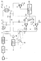
- Fig. 9 shows another example of a specific circuit arrangement of the main portion of Fig. 6, and in Fig. 9, like parts corresponding to those of Figs. 6 and 7 are marked with the same references and therefore need not be described in detail.
- one end of the primary side winding of the conversion transformer 4 is connected to the rectifying circuit 5 and the other end thereof is connected to the collector of an output transistor Tr1 which forms the control circuit 6.
- the emitter of the transistor Tr1 is grounded and the base thereof is connected to an output terminal of a pulse width modulation control circuit (hereinafter referred to as a PWM control circuit) 6a.
- the collector of the transistor Tr2 such as the photo transistor forming the photo coupler 7 is connected to the input terminal of the PWM control circuit 6a and the emitter thereof is grounded.
- Light from a light emitting element CD1 formed of the light emission diode or the like forming the photo coupler 7 is supplied to the base of the transistor Tr2.
- An anode of a light emitting element CD1 is connected to the positive terminal 13 to which the anode of the secondary battery 12 to be charged is connected.
- a cathode of the light emitting element CD1 is connected through the resistor R1 to anodes of diodes CD19 and CD20 the cathodes of which are respectively connected to output terminals of an output voltage error detecting operational amplifier 17 and an output current error detecting operational amplifier 18 forming the output control circuit 8.
- a smoothing circuit 5a formed of the diode CD18, a capacitor C1 or the like is provided at the secondary winding side of the conversion transformer 4. One end of its secondary winding is grounded and the other end thereof is connected to the anode of the diode CD18.
- the cathode of the diode CD18 is connected to one end of the capacitor C1 and is also connected to the positive terminal 13 to which the secondary battery 12 is connected.
- the other end of the capacitor C1 is grounded, and the charging current detection resistor 15 is connected to the negative terminal 14 to which the cathode of the secondary battery 12 is connected.
- One end of the resistor 15 is grounded, and a charging current developed at a junction 71 between the resistor 15 and the negative terminal 14 is supplied to non-inverting input terminals of the output current error detection operational amplifier 18 forming the constant current control means and the charging current detection operational amplifier 19.
- Reference current sources E3 and E4 are connected to the inverting input terminals of these operational amplifiers 18 and 19.
- a voltage developed at a junction 72 between the diode CD18 and the positive terminal 13 is divided by the resistors R16 and R17 and fed to the non-inverting input terminal of the output voltage error detection operational amplifier 17 which forms the constant voltage control means.
- An inverting input terminal of the operational amplifier 17 is connected through a switch SW to, for example, two reference voltage sources E1 and E2.
- the number of the reference voltage sources E1 and E2 is not limited to two and a plurality of reference voltage sources may be provided depending on the number of the charging state detection points as will described later. Further, the two reference voltage sources E1 and E2 need not be selectively switched by the switch SW, and alternatively, it is possible to provide a voltage varying means which continuously varies the voltage of one reference voltage source.
- the switch SW or the voltage varying means is controlled by the output of a CPU 10B.
- the CPU 10B incorporates therein a digital-to-analog converting means, an analog-to-digital converting means or the like, whereby the control signal which controls the switch SW is converted to an analog control signal and an analog charging current from the charging current detection operational amplifier 19 is converted to a digital signal and fed to the CPU 10B.
- the outputs of the operational amplifiers 17 and 18 are supplied to cathodes of the diodes CD19 and CD20, respectively.
- an AC voltage from the commercially available AC power supply source is converted to a DC voltage by means of the input filter 2, the rectifying circuit 5, the switching section 6, the conversion transformer 4 and the smoothing circuit 5a and this charging voltage is supplied to the secondary battery 12.
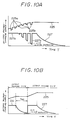
- the operational amplifier 18 compares the charging current flowing through the resistor 15 with the reference current of the reference current source E3, and an output error current from the operational amplifier 18 is supplied to the light emitting element CD1 forming the photo coupler 7 through the diode CD20 to drive the apparatus in a constant current in such a fashion that, as shown by a constant current curve 227a of a rapid charging current characteristic curve 227 in Fig. 10A, a constant current becomes 2A.
- the operational amplifier 17 compares the rectified DC voltage (output voltage) supplied to the secondary battery 12 with the reference voltage of the second reference voltage source E2, and supplies an output error voltage thereof to the light emitting element CD1 forming the photo coupler 7 through the diode CD19 to drive the apparatus in the constant voltage fashion such that, as shown by, for example, a rapid charging battery voltage characteristic curve 225, an output voltage 225a becomes 8.3V.
- the error signals of the two operational amplifiers 17 and 18 are supplied through the light receiving element Tr1 to the PWM control circuit 6a connected to the primary winding side of the conversion transformer 4 by the photo coupler 7 so as to control the outputs of the charging voltage and the charging current to become constant via the conversion transformer 4.
- the operational amplifier 19 detects the charging current flowing through the charging resistor 15 and compares the detected charging current with the reference current of the reference current source E4 to thereby supply a very small charging current to the CPU 10B.
- the CPU 10B determines whether this very small charging current is less than a predetermined value, e.g., 0.1A or not.
- the output voltage 225a supplied to the secondary battery 12 is 8.3 V when the voltage of the second reference voltage source E2 connected to a second fixed contact c of the switch SW connected to the inverting input terminal of the operational amplifier 17 is V2 volts. Also, let it be assumed that the battery release voltage is 7.5V when the secondary battery 12 is charged to the 50% charging state. Then, the voltage of the first reference voltage source E1 to which the movable contact a of the switch SW is connected via a first fixed contact b is selected to be V1 volts and this voltage V1 of the first reference voltage source E1 is selected such that the output voltage 225b supplied to the secondary battery 12 becomes nearly equal to 7.5V.
- the CPU 10B derives a control signal 10a which changes over the switch SW at a predetermined cycle as shown in Fig. 10A.
- the operational amplifier 19 detects the charging current and the detected charging current is supplied to the CPU 10B. If the charging current is higher than 0.1 A, the CPU 10B changes the movable contact a of the switch SW to the V2 volt (output voltage 8.5V) side, ie reference voltage source E2 side, to thereby charge the secondary battery 12 by a charging current 2A during a predetermined period of time.
- the charging current with the battery release voltage of 7.5V corresponding to the 50 % charging state gradually decreases from 2A and when it decreases to 0.1A, it can be determined that the secondary battery 12 is charged to the 50 % charging state. Also, when a plurality of charging states, such as a 30% charging state, a 70% charging state and so on are detected in addition to the detection of the 50% charging state, the voltage of the reference voltage source E2 is set to an appropriate value and the switch SW is switched accordingly, in a similar fashion to that described above.
- the charging time for achieving the 50% charging state can be reduced.
- the secondary battery has the rapid charging battery voltage characteristic curve 225 and the rapid charging current characteristic curve 227 shown in Fig. 10B.
- the charging time is similar to that of the charging method shown in Fig. 10A when the charging current is 2A, and it takes a lot of time for the charging current to decrease to 0.1A. Accordingly, if the secondary battery is charged by the charging voltage higher than 7.5V, i.e., 8.5V until the charging current begins to decrease and reaches 0.1A, then the charging current recovers to 2A.
- the time T50 of Fig. 10B can be considerably reduced by the time in which the charging voltage is selected to be 8.5V.
- the switching means of large current capacity shown in Figs. 4A and 4B are not needed and detection accuracy in detecting the battery voltage can be increased.
- the battery voltage measuring circuit and the charging current detecting circuit for detecting the end of charging operation are both required in order to detect the release voltage of the secondary battery and to detect or display the charging state in the prior art
- a circuit for detecting the voltage is not needed because the output voltage is merely set and only the charging current detecting circuit of the operational amplifier 19 is required.
- the charging state can be detected by the charging current detecting circuit which detects the end of the charging operation so that the circuit arrangement can be simplified.
- the battery voltage can be detected with high accuracy and the circuit arrangement can be simplified considerably.
Landscapes
- Engineering & Computer Science (AREA)
- Power Engineering (AREA)
- Physics & Mathematics (AREA)
- General Physics & Mathematics (AREA)
- Charge And Discharge Circuits For Batteries Or The Like (AREA)
- Secondary Cells (AREA)
Claims (5)
- Appareil de charge pour la charge à tension constante d'une batterie d'accumulateurs (12), l'appareil comprenant un moyen de réglage de tension (8) pour régler la tension constante pour charger la batterie à un certain nombre de valeurs différentes, dans l'ordre des tensions croissantes, caractérisé en ce que :
chacune desdites valeurs de tension est associée à un état de charge de la batterie (12), prédéterminé, qui doit être détecté, et en ce que l'appareil comprend un moyen de détection (10) pour détecter une chute prédéterminée du courant de charge, au cours d'une charge à tension constante, à chaque valeur de tension indiquant que l'état de charge associé a été atteint, dans lequel, en réponse à la détection du fait que ledit état de charge a été atteint, le moyen de détection (10) commande un affichage (11) pour indiquer l'état de charge, et si l'état de charge complet n'a pas été atteint, le moyen de réglage de tension (8) change la valeur de tension constante pour la valeur suivante, plus élevée. - Appareil selon la revendication 1, dans lequel, à chaque valeur de tension, le moyen de réglage de tension (8) est agencé pour commuter le niveau de tension entre un niveau de tension permettant une charge rapide et ladite valeur de tension pour charge à tension constante, et dans lequel le moyen de détection (10) détecte l'état de charge lorsque le niveau de tension est commuté vers ladite valeur de tension.
- Appareil selon la revendication 2, incluant un moyen de détection d'erreur de tension de sortie (17) pour commander la charge à tension constante de la batterie (12).
- Appareil selon la revendication 3, incluant un moyen de détection d'erreur de courant de sortie (18) pour commander la charge à courant constant de la batterie (12).
- Appareil selon la revendication 3 ou la revendication 4, dans lequel, le moyen de réglage de tension (8) commute une source de tension de référence (E₁, E₂) du moyen de détection d'erreur de tension de sortie (17) pour effectuer la commutation de niveau de tension.
Applications Claiming Priority (4)
| Application Number | Priority Date | Filing Date | Title |
|---|---|---|---|
| JP2046814A JP3019353B2 (ja) | 1990-02-27 | 1990-02-27 | 充電装置 |
| JP46814/90 | 1990-02-27 | ||
| JP2046812A JPH03251052A (ja) | 1990-02-27 | 1990-02-27 | 充電量表示装置 |
| JP46812/90 | 1990-02-27 |
Publications (3)
| Publication Number | Publication Date |
|---|---|
| EP0448235A2 EP0448235A2 (fr) | 1991-09-25 |
| EP0448235A3 EP0448235A3 (en) | 1992-07-15 |
| EP0448235B1 true EP0448235B1 (fr) | 1995-08-23 |
Family
ID=26386941
Family Applications (1)
| Application Number | Title | Priority Date | Filing Date |
|---|---|---|---|
| EP91301515A Expired - Lifetime EP0448235B1 (fr) | 1990-02-27 | 1991-02-26 | Chargeur de batterie |
Country Status (4)
| Country | Link |
|---|---|
| US (1) | US5172044A (fr) |
| EP (1) | EP0448235B1 (fr) |
| DE (1) | DE69112243T2 (fr) |
| MY (1) | MY104792A (fr) |
Families Citing this family (42)
| Publication number | Priority date | Publication date | Assignee | Title |
|---|---|---|---|---|
| US5304917A (en) * | 1990-11-30 | 1994-04-19 | Burr-Brown Corporation | Compact low noise low power dual mode battery charging circuit |
| TW226496B (en) * | 1992-07-21 | 1994-07-11 | Sanyo Denki Kk | Battery charger |
| JP2741139B2 (ja) * | 1992-09-10 | 1998-04-15 | ローム株式会社 | 蓄電池充電回路 |
| US5656920A (en) * | 1992-10-13 | 1997-08-12 | Gnb Battery Technologies, Inc. | Method and apparatus for charging a lead-acid battery |
| JP3384027B2 (ja) * | 1993-05-14 | 2003-03-10 | ソニー株式会社 | 充電方法および充電器 |
| US5592068A (en) * | 1993-05-28 | 1997-01-07 | William E. Gregory | Lead acid battery rejuvenator |
| US5583416A (en) * | 1994-01-26 | 1996-12-10 | Gnb Battery Technologies, Inc. | Apparatus and method for step-charging batteries to optimize charge acceptance |
| JPH07235332A (ja) * | 1994-02-24 | 1995-09-05 | Sanyo Electric Co Ltd | 二次電池の充電方法 |
| US5640080A (en) * | 1994-07-29 | 1997-06-17 | Sanyo Electric Co., Ltd. | Secondary battery charger |
| US5648714A (en) * | 1994-11-30 | 1997-07-15 | 3266991 Manitoba Ltd. | Method and device for charging and conditioning batteries |
| US5581170A (en) * | 1994-12-12 | 1996-12-03 | Unitrode Corporation | Battery protector |
| US5652501A (en) * | 1994-12-12 | 1997-07-29 | Unitrode Corporation | Voltage sensor for detecting cell voltages |
| KR0158109B1 (ko) * | 1994-12-28 | 1998-12-15 | 김광호 | 재 충전용 밧데리의 충전제어 방법 및 회로 |
| DE19609140A1 (de) * | 1996-03-08 | 1997-09-18 | Nokia Mobile Phones Ltd | Ladeschaltung |
| JP3911049B2 (ja) * | 1996-07-16 | 2007-05-09 | ソニー株式会社 | 充電装置 |
| US5646506A (en) * | 1996-08-21 | 1997-07-08 | Suzuki; Takeshi | Method of charging a secondary battery and an apparatus therefor |
| US5994879A (en) * | 1999-03-01 | 1999-11-30 | Ma Lien Electrical Engineering Co., Ltd. | Charging circuit |
| DE10110642B4 (de) * | 2000-03-13 | 2005-06-16 | Nippon Telegraph And Telephone Corp. | Kapazitätsabschätzungsverfahren, Degradationsabschätzungsverfahren und Degradationsabschätzungsvorrichtung für Lithium-Ionenzellen und Lithium-Ionenbatterien |
| TW510977B (en) | 2000-03-13 | 2002-11-21 | Nippon Telegraph & Telephone | Capacity estimation method, degradation estimation method and degradation estimation apparatus for lithium-ion cells, and lithium-ion batteries |
| US6822425B2 (en) * | 2002-01-25 | 2004-11-23 | Vector Products, Inc. | High frequency battery charger and method of operating same |
| JP3832426B2 (ja) * | 2002-12-10 | 2006-10-11 | ソニー株式会社 | 二次電池、表示方法、記録媒体、並びにプログラム |
| US7876068B2 (en) * | 2003-10-24 | 2011-01-25 | International Components Corporation | Battery charge indicator |
| KR100542215B1 (ko) * | 2003-12-23 | 2006-01-10 | 삼성에스디아이 주식회사 | 2차 전지의 충전방법 및 충전장치 |
| DE102005020356A1 (de) * | 2005-05-02 | 2006-11-09 | Robert Bosch Gmbh | Vorrichtung, insbesondere Ladegerätvorrichtung |
| JP4486618B2 (ja) * | 2006-06-06 | 2010-06-23 | 株式会社リコー | 充電回路、充電回路の動作制御方法及び電源装置 |
| EP2092628A4 (fr) * | 2006-11-27 | 2013-04-03 | Universal Supercapacitors Llc | Procédé de charge de condensateurs électrochimiques possédant une double couche électrique |
| WO2009146064A2 (fr) * | 2008-04-01 | 2009-12-03 | William Baker | Chargeurs de batterie à multiples baies et circuit |
| US9419457B2 (en) | 2012-09-04 | 2016-08-16 | Google Technology Holdings LLC | Method and device with enhanced battery capacity savings |
| US20140077754A1 (en) * | 2012-09-18 | 2014-03-20 | Charger Coach Llc | System and Method For Scheduling Lithium Ion Battery Charging |
| US9356461B2 (en) * | 2012-09-25 | 2016-05-31 | Google Technology Holdings, LLC | Methods and systems for rapid wireless charging where the low state of charge (SOC) temperature dependent charging current and low SOC temperature limit are higher than the high SOC temperature dependent charging current and high SOC temperature limit |
| JP2014137272A (ja) * | 2013-01-16 | 2014-07-28 | Denso Corp | 電圧監視装置 |
| US9491706B2 (en) | 2013-03-13 | 2016-11-08 | Google Technology Holdings LLC | Reduced-power transmitting from a communications device |
| US9124101B2 (en) * | 2013-04-02 | 2015-09-01 | Bel Fuse (Macao Commercial Offshore) Limited | Power supply having selectable operation based on communications with load |
| US9596653B2 (en) | 2013-12-16 | 2017-03-14 | Google Technology Holdings LLC | Remedying power drain via a coverage map |
| US9865897B2 (en) | 2014-06-02 | 2018-01-09 | Google Llc | Stacked electrochemical cell with increased energy density |
| US9438293B2 (en) | 2014-08-05 | 2016-09-06 | Google Technology Holdings LLC | Tunable circuit elements for dynamic, per element power |
| US9472965B2 (en) | 2014-09-08 | 2016-10-18 | Google Technology Holdings LLC | Battery cycle life through smart overnight charging |
| US11437829B2 (en) | 2016-03-07 | 2022-09-06 | The Regents Of The University Of Michigan | Method to charge lithium-ion batteries with user, cell and temperature awareness |
| WO2018012151A1 (fr) * | 2016-07-12 | 2018-01-18 | Necエナジーデバイス株式会社 | Dispositif de traitement d'informations, procédé de commande, et programme |
| US11258285B2 (en) | 2017-06-06 | 2022-02-22 | The Regents Of The University Of Michigan | User aware charging algorithm that reduces battery fading |
| US10594158B2 (en) * | 2017-07-26 | 2020-03-17 | Quanta Computer Inc. | ORing FET control method for battery backup system |
| DE102018210524A1 (de) * | 2018-06-27 | 2020-01-02 | Robert Bosch Gmbh | Verfahren zum Aufladen von Akkupacks für Elektrowerkzeugmaschinen sowie Ladegerät zur Durchführung des Verfahrens |
Citations (1)
| Publication number | Priority date | Publication date | Assignee | Title |
|---|---|---|---|---|
| EP0349995A2 (fr) * | 1988-07-04 | 1990-01-10 | ELEKTRON-BREMEN Fabrik für Elektrotechnik GmbH | Procédé d'adaptation d'un chargeur de batterie à différents procédés de charge et types de batterie et chargeur |
Family Cites Families (11)
| Publication number | Priority date | Publication date | Assignee | Title |
|---|---|---|---|---|
| US3854082A (en) * | 1973-06-07 | 1974-12-10 | Master Control Syst Inc | Battery charging circuit |
| FR2239772A1 (en) * | 1973-07-03 | 1975-02-28 | Scient Electric | Battery charger with initial intensive charging - has final reduced charging with intermediate charging by switching between charging states |
| FR2326052A1 (fr) * | 1975-09-26 | 1977-04-22 | Accumulateurs Fixes | Methode et dispositif de charge pour les batteries d'accumulateurs |
| GB2086674B (en) * | 1980-10-29 | 1984-08-30 | Harmer & Simmons Ltd | Battery charging apparatus |
| US4418310A (en) * | 1981-11-18 | 1983-11-29 | Hobart Brothers Company | Battery charger control circuit |
| DE3227522C2 (de) * | 1982-07-23 | 1985-05-09 | Stubbe electronic Paul K. Stubbe GmbH & Co, 6000 Frankfurt | Verfahren und Vorrichtung zum Schnelladen von Nickelcadmium-Akkumulatoren und gleichzeitigem Überwachen der eingeladenen Gesamtkapazität |
| DE3429673A1 (de) * | 1984-08-11 | 1986-02-20 | Robert Bosch Gmbh, 7000 Stuttgart | Verfahren und vorrichtung zum schnelladen einer batterie |
| JPS61170678A (ja) * | 1985-01-25 | 1986-08-01 | Nissan Motor Co Ltd | バツテリ状態検知装置 |
| US4629965A (en) * | 1985-02-26 | 1986-12-16 | General Battery Corporation | Battery charger termination circuit |
| JPS61147552U (fr) * | 1985-03-05 | 1986-09-11 | ||
| US4918368A (en) * | 1986-10-29 | 1990-04-17 | Span, Inc. | System for charging batteries and measuring capacities and efficiencies thereof |
-
1991
- 1991-02-25 MY MYPI91000302A patent/MY104792A/en unknown
- 1991-02-25 US US07/660,001 patent/US5172044A/en not_active Expired - Fee Related
- 1991-02-26 EP EP91301515A patent/EP0448235B1/fr not_active Expired - Lifetime
- 1991-02-26 DE DE69112243T patent/DE69112243T2/de not_active Expired - Lifetime
Patent Citations (1)
| Publication number | Priority date | Publication date | Assignee | Title |
|---|---|---|---|---|
| EP0349995A2 (fr) * | 1988-07-04 | 1990-01-10 | ELEKTRON-BREMEN Fabrik für Elektrotechnik GmbH | Procédé d'adaptation d'un chargeur de batterie à différents procédés de charge et types de batterie et chargeur |
Also Published As
| Publication number | Publication date |
|---|---|
| EP0448235A2 (fr) | 1991-09-25 |
| DE69112243D1 (de) | 1995-09-28 |
| MY104792A (en) | 1994-05-31 |
| DE69112243T2 (de) | 1996-02-15 |
| EP0448235A3 (en) | 1992-07-15 |
| US5172044A (en) | 1992-12-15 |
Similar Documents
| Publication | Publication Date | Title |
|---|---|---|
| EP0448235B1 (fr) | Chargeur de batterie | |
| US5408170A (en) | Device for charging a secondary battery having interrupt means to prevent overcharging | |
| US5621302A (en) | Battery charger monitoring battery voltage and/or temperature at relevant sampling interval | |
| US5541491A (en) | Battery charging apparatus | |
| US5726552A (en) | Method and apparatus for controlling charging of electrical power storage unit | |
| JP3416952B2 (ja) | 電源残余容量測定装置および電源残余容量測定回路を備えた電源装置 | |
| US4290002A (en) | Method and apparatus for controlling battery recharging | |
| KR100275140B1 (ko) | 충전장치 | |
| US5412307A (en) | Residual capacity indicating device | |
| JP3096535B2 (ja) | 二次電池の充電方法及び充電装置 | |
| JPH05336679A (ja) | 二次電池の充電回路 | |
| JP3074694B2 (ja) | 充電装置 | |
| KR100201445B1 (ko) | 충전량표시장치 | |
| JP3505747B2 (ja) | 充電装置 | |
| EP1435683A2 (fr) | Dispositif électronique comportant une unité de charge de batteries | |
| JP2000134820A (ja) | 充電装置における充電方式 | |
| JPH1042484A (ja) | 充電装置 | |
| JPH05336675A (ja) | 二次電池の充電回路 | |
| KR930009601B1 (ko) | 밧데리 충전제어 회로 | |
| JPH06213981A (ja) | 充放電システム | |
| KR0151494B1 (ko) | 충전 가능한 배터리의 충전 모드 변환 회로 | |
| JP2635346B2 (ja) | 充電制御装置 | |
| KR100258818B1 (ko) | 2차 전지의 충방전 시험기 회로 | |
| JP3286861B2 (ja) | 高圧電源装置 | |
| JPH05336674A (ja) | 二次電池の充電回路 |
Legal Events
| Date | Code | Title | Description |
|---|---|---|---|
| PUAI | Public reference made under article 153(3) epc to a published international application that has entered the european phase |
Free format text: ORIGINAL CODE: 0009012 |
|
| AK | Designated contracting states |
Kind code of ref document: A2 Designated state(s): DE FR GB |
|
| PUAL | Search report despatched |
Free format text: ORIGINAL CODE: 0009013 |
|
| AK | Designated contracting states |
Kind code of ref document: A3 Designated state(s): DE FR GB |
|
| 17P | Request for examination filed |
Effective date: 19921022 |
|
| 17Q | First examination report despatched |
Effective date: 19940325 |
|
| GRAA | (expected) grant |
Free format text: ORIGINAL CODE: 0009210 |
|
| AK | Designated contracting states |
Kind code of ref document: B1 Designated state(s): DE FR GB |
|
| REF | Corresponds to: |
Ref document number: 69112243 Country of ref document: DE Date of ref document: 19950928 |
|
| ET | Fr: translation filed | ||
| PLBE | No opposition filed within time limit |
Free format text: ORIGINAL CODE: 0009261 |
|
| STAA | Information on the status of an ep patent application or granted ep patent |
Free format text: STATUS: NO OPPOSITION FILED WITHIN TIME LIMIT |
|
| 26N | No opposition filed | ||
| REG | Reference to a national code |
Ref country code: GB Ref legal event code: IF02 |
|
| REG | Reference to a national code |
Ref country code: GB Ref legal event code: 746 Effective date: 20091124 |
|
| PGFP | Annual fee paid to national office [announced via postgrant information from national office to epo] |
Ref country code: FR Payment date: 20100226 Year of fee payment: 20 |
|
| PGFP | Annual fee paid to national office [announced via postgrant information from national office to epo] |
Ref country code: DE Payment date: 20100219 Year of fee payment: 20 Ref country code: GB Payment date: 20100218 Year of fee payment: 20 |
|
| REG | Reference to a national code |
Ref country code: DE Ref legal event code: R071 Ref document number: 69112243 Country of ref document: DE |
|
| REG | Reference to a national code |
Ref country code: GB Ref legal event code: PE20 Expiry date: 20110225 |
|
| PG25 | Lapsed in a contracting state [announced via postgrant information from national office to epo] |
Ref country code: GB Free format text: LAPSE BECAUSE OF EXPIRATION OF PROTECTION Effective date: 20110225 |
|
| PG25 | Lapsed in a contracting state [announced via postgrant information from national office to epo] |
Ref country code: DE Free format text: LAPSE BECAUSE OF EXPIRATION OF PROTECTION Effective date: 20110226 |