EP0448776A2 - Regelungssystem für die Ausgangsenergie einer Pulslichtquelle - Google Patents
Regelungssystem für die Ausgangsenergie einer Pulslichtquelle Download PDFInfo
- Publication number
- EP0448776A2 EP0448776A2 EP90117953A EP90117953A EP0448776A2 EP 0448776 A2 EP0448776 A2 EP 0448776A2 EP 90117953 A EP90117953 A EP 90117953A EP 90117953 A EP90117953 A EP 90117953A EP 0448776 A2 EP0448776 A2 EP 0448776A2
- Authority
- EP
- European Patent Office
- Prior art keywords
- light
- signal
- output
- comparator
- control
- Prior art date
- Legal status (The legal status is an assumption and is not a legal conclusion. Google has not performed a legal analysis and makes no representation as to the accuracy of the status listed.)
- Granted
Links
Images




Classifications
-
- H—ELECTRICITY
- H01—ELECTRIC ELEMENTS
- H01S—DEVICES USING THE PROCESS OF LIGHT AMPLIFICATION BY STIMULATED EMISSION OF RADIATION [LASER] TO AMPLIFY OR GENERATE LIGHT; DEVICES USING STIMULATED EMISSION OF ELECTROMAGNETIC RADIATION IN WAVE RANGES OTHER THAN OPTICAL
- H01S3/00—Lasers, i.e. devices using stimulated emission of electromagnetic radiation in the infrared, visible or ultraviolet wave range
- H01S3/10—Controlling the intensity, frequency, phase, polarisation or direction of the emitted radiation, e.g. switching, gating, modulating or demodulating
- H01S3/13—Stabilisation of laser output parameters, e.g. frequency or amplitude
- H01S3/131—Stabilisation of laser output parameters, e.g. frequency or amplitude by controlling the active medium, e.g. by controlling the processes or apparatus for excitation
- H01S3/134—Stabilisation of laser output parameters, e.g. frequency or amplitude by controlling the active medium, e.g. by controlling the processes or apparatus for excitation in gas lasers
-
- B—PERFORMING OPERATIONS; TRANSPORTING
- B23—MACHINE TOOLS; METAL-WORKING NOT OTHERWISE PROVIDED FOR
- B23K—SOLDERING OR UNSOLDERING; WELDING; CLADDING OR PLATING BY SOLDERING OR WELDING; CUTTING BY APPLYING HEAT LOCALLY, e.g. FLAME CUTTING; WORKING BY LASER BEAM
- B23K26/00—Working by laser beam, e.g. welding, cutting or boring
- B23K26/70—Auxiliary operations or equipment
- B23K26/702—Auxiliary equipment
-
- H—ELECTRICITY
- H01—ELECTRIC ELEMENTS
- H01S—DEVICES USING THE PROCESS OF LIGHT AMPLIFICATION BY STIMULATED EMISSION OF RADIATION [LASER] TO AMPLIFY OR GENERATE LIGHT; DEVICES USING STIMULATED EMISSION OF ELECTROMAGNETIC RADIATION IN WAVE RANGES OTHER THAN OPTICAL
- H01S3/00—Lasers, i.e. devices using stimulated emission of electromagnetic radiation in the infrared, visible or ultraviolet wave range
- H01S3/10—Controlling the intensity, frequency, phase, polarisation or direction of the emitted radiation, e.g. switching, gating, modulating or demodulating
- H01S3/13—Stabilisation of laser output parameters, e.g. frequency or amplitude
- H01S3/131—Stabilisation of laser output parameters, e.g. frequency or amplitude by controlling the active medium, e.g. by controlling the processes or apparatus for excitation
Definitions
- the present invetnion relates to pulsed light sources such as a pulsed laser light generating apparatus, and more particularly to control of the output energy of such pulsed light sources.
- an excimer laser can provide strong oscillation beams with several wavelengths in a range of 353 nm to 193 nm with halogen gas such as fluorine and chlorine being combined with noble gas such as krypton and xenon which is a laser medium.
- This excimer laser is one of pulsed lasers and arranged such that the gas which is the laser medium is excited by quickly discharging charge in capacitor or the like to produce laser light.
- the duration of the laser light is several times of 10 nanoseconds and the oscillation repeatedly occurs with a period of several milliseconds to several times of 10 milliseconds.
- an important problem is to control the emission energy per one pulse to an adequate value.
- the energy per one pulse is below a given threshold, a material to be machined is not changed at all irrespective of continuous illumination of the laser light so that the machining effect doest not appear.
- the pulse energy exceeds a predetermined value, portions other than the light-receiving portion is undesirably subjected to deformation, decomposition and deterioration.
- the excimer laser has a characteristic that the output energy is monotonously lowered with long-time operation because of deterioration of the gas which is the laser medium and the efficiency varies for a relatively short time due to generation of impurities and others. This requires a means to keeping the pulse intensity to a set value by adjusting the output voltage of a high voltage power supply at all times.
- a pulsed light source is generally arranged such that the apparent pulse strength becomes constant by keeping the average output to a constant value as disclosed in USP 4,611,270.
- a conventional pulsed light source will be described hereinbelow with reference to Fig. 1.
- a light-emitting section (pulsed laser) 1 intermittently emits light in response to supply of an electric energy from a power supply 2.
- a portion of light emitted from the light-emitting section 1 is derived through a half mirror or beam splitter 4 and then led to a light-receiving element (photodetector) 5.
- the light-receiving element 5 produces an electric signal corresponding to the intensity of the incident light thereon and supplies it through an averaging circuit 6 to a comparator 7.
- the comparator 7 compares a reference value Vr with the value of a signal corresponding to the laser output time-averaged in the averaging circuit 6 so as to control the power supply 2 in accordance with the difference therebetween.
- operation of the convetnional pulsed light source will be described hereinbelow with reference to Fig. 2.
- Fig. 2 first, the light-emitting section 1 oscillates with a constant period as illustrated.
- the comparator operates so that the pulse energy becomes great.
- the conventional system causes generation of substandard products because of being difficult to keep constant the pulse energy.
- the conventional control system is arranged to compensate for the output lowering due to relative long time operation and generally arranged such that the time constant of the averaging circuit takes about several second order.
- a pulsed light source comprising: light-emitting means for emitting light in pulse form; power supply means for supplying an electric power to the light-emitting means, the magnitude of the electric power being changeable in response to a control signal; light-receiving means responsive to light from the light-emitting means so as to produce an electric signal corresponding to the intensity of the reception light; and comparator means coupled to the light-receiving means so as to compare the electric signal therefrom with a reference signal to output a signal proportional to the difference between the electric signal and the reference signal; and control means responsive to the output signal of the comparator means so as to produce the control signal, which is supplied to the power supply means to control the electric power outputted from the power supply means to the light-emitting means.
- the comparator means and the control means are coupled through switching means to each other whereby the output signal of the comparator means is connected and disconnected with respect to the control means.
- the switching means is arranged to take a closed state for a predetermined time period in synchronism with the emission of the light-emitting means.
- the output signal of the comparator means is amplified with a gain which is below 1 and the control means produces the control signal in accordance with the amplified signal.
- the gain of the comparator means is variable in accordance with variation of the light emitted from the light-emitting means.
- a pulsed light source comprising: light-emitting means for emitting light in pulse form; power supply means for supplying an electric power to the light-emitting means, the power supply means being controllable in accordance with a digital control signal; light-receiving means responsive to the light emitted from the light-emitting means so as to generate an electric signal corresponding to the intensity of the reception light therefrom; comparator means coupled to the light-receiving means so as to compare the output signal of the light-receiving means with a reference signal to output a signal corresponding to the difference therebetween; and control means coupled to the comparator means to digitize the output signal of the comparator means and add the digitized signal to a predetermined digital signal, thereby producing the digital control signal to be supplied to the power supply means.
- the pulsed light source includes a light-emitting section (laser) 1 which outputs light in a pulse form in response to supply of a power from a high voltage power supply 2.
- a portion of the output light of the light-emitting section 1 is derived through a beam splitter 4 and received by means of a photodetector 5.
- the photodetector 5 generates an electric signal corresponding to the energy of the reception light and outputs it to a peak detector 8.
- the output of the peak detector 8 is supplied to a comparator 7 which compares the output voltage of the peak detector 8 with a predetermined reference value Vr so as to generate a difference signal ⁇ V in accordance with the comparison result, i.e., in correspondance with the difference therebetween.
- the output signal of the comparator 7 is led to a divider 20 so as to regulate the difference signal ⁇ V to a small signal ⁇ s which is proportional thereto.
- the output signal ⁇ s of the divider 20 is led through switch 21 to an integrating circuit 9.
- the switch 21 is arranged to be closed by means of a synchronous circuit 3 for a predetermined time period ts after emission due to the light-emitting section 1.
- the integrating circuit 9 adds the samll signal ⁇ s to its output voltage V0.
- the power supply 2 supplies the light-emitting section 1 with a voltage V which is proportional to the output voltage V0 of the integrating circuit 9.
- the pulse energy P starts to decrease while the light-emitting section 1 continuously operates to emits light in a pulse form.
- the photodetector 5 In response to a portion of the output light of the light-emitting section 1, the photodetector 5 generates a voltage signal proportional to the energy of the reception light therefrom. Because of having a pulse form, if the voltage signal is compared with the reference voltage Vr which is a direct-current voltage signal, a great error occurs during a time in which the light-emitting section 1 does not emit the light.
- the peak detector 8 holds the voltage proportional to the reception pulse energy of the photodetector 5 until the next pulse emission of the light-emitting section 1 and produces a direct-current signal Vdc corresponding thereto.
- the integrating circuit 9 generates the signal V0 by charge stored in a capacitor 91.
- the small signal ⁇ s produced by dividing the difference signal ⁇ V by means of the divider 20 is added to the voltage of the capacitor 91 only for a predetermined time ts, whereby the output voltage V of the power supply 2 varies in the direction that the pulse output returns to a predetermined value.
- the light-emitting section 1 is a pulsed laser such as an excimer laser
- the energy of the output light varies at every emission.
- the divider 20 is for the purpose of no amplification of the variation under the energy control. That is, the comparator 7 requires that the output voltage of the power supply 2 is increased by ⁇ V1 at the time of the next emission.
- the output of the light-emitting section 1 fluctuates, even if the output voltage of the power supply 2 is increased by ⁇ V1, the output energy does not necessarily become a predetermined value. According to experiments by the inventors, the increase of the output voltage of the power supply 2 rather causes the output fluctuation to become greater.
- the capacitor 91 Into the capacitor 91 is introduced charge proportional to an amount obtained by multiply the samll signal ⁇ s by a time ts for which the switch 21 is in the closed condition. If there is not provided the switch 21, the time ts is equal to the period of the emission. At this time, since the charge additionally introduced into the capacitor 91 is not only proportional to the difference signal but also proportional to the emission period, when the emission interval varies, the controlled amount varies in accordance with the emission period. In the case that the time ts is kept to be constant through the switch 21, it is possible to control the energy to a constant value irrespective of the emission period.
- Fig. 4 The energy control will be described hereinbelow with reference to Fig. 4.
- the efficiency of the light-emitting section 1 starts to decrease from time t1 and, in order to clearly show the effect of this invention, the control to make the energy constant is not performed until time t2 whereby the pulse energy varies and the average value thereof decreases in accordance with the decrease in the efficiency.
- the pulse energy control is started.
- the comparator 7 compares the reference signal Vr with the direct-current signal Vdc proportional to the pulse energy immediately before the time t2 so as to output the small signal ⁇ s to the integrating circuit 9.
- the integrating circuit 9 controls the power supply 2 so that the difference can be cancelled, that is, if the small signal ⁇ s is positive, the output voltage V of the power supply 2 is controlled to be increased, and if ⁇ s is negative, V is decreased. Therefore, at the time of the next emission, the pulse energy approaches the predetermined value. Thereafter, the pulse strength is controlled to direct to the predetermined value at every emission and therefore the average value of the pulse energies directs to a predetermined value.
- the emission period is shortened from time t3.
- the time ts for which the small signal ⁇ s is supplied to the integrating circuit 9 is independent on the emission period, and therefore the pulse energy can be kept constant as well as before time t3.
- the peak value of the pulse strength is held, it is also appropriate to hold the integrated value of the pulse waveform. Further, it is appropriate to use a sample and hold circuit, which is a general IC circuit, instead of the peak detector 8.
- the divider 20 is not necessarily provided independently, and it is also appropriate to reduce the gain of the peak detector 8 or the comparator 7.
- the synchronous circuit 3 is not limited to the description. it is also appropriate to detect the emission in conjunction with the power supply 2, the light-emitting section 1 and the photodetector 5.
- a pulsed light source of this embodiment similarly includes a light-emitting section (laser) 1 which outputs light in a pulse form in response to supply of a power from a high voltage power supply 2.
- a portion of the output light of the light-emitting section 1 is derived through a beam splitter 4 and received by means of a photodetector 5.
- the photodetector 5 generates an electric signal corresponding to the energy of the reception light and outputs it to a peak detector 8.
- the output of the peak detector 8 is supplied to a comparator 7 which compares the output voltage of the peak detector 8 with a predetermined reference value Vr so as to generate a difference signal ⁇ V in accordance with the comparison result, i.e., in correspondance with the difference therebetween.
- the output signal of the comparator 7 is led to a divider 20 so as to regulate the difference signal ⁇ V to a small signal ⁇ s which is proportional thereto.
- the output signal ⁇ s of the divider 20 is led to an analog-to-digital (A/D) converter 11 the output of which is supplied to an adder 12 so as to take the sum of the output of the A/D converter 11 and a voltage [V0] for setting the output of the power supply 2.
- the sum signal is led to a latch 13.
- the voltage [V0] is a digital voltage obtained by the analog-to-digital conversion of the voltage V0.
- the output of the latch 13 is supplied to a digital-to-analog converter (D/A) 14 so as to become an output setting voltage V0.
- D/A digital-to-analog converter
- the operation timings of the A/D converter 11 and the latch 13 are determined in accordance with signals from the synchronous circuit 3.
- the pulse energy P starts to decrease while the light-emitting section 1 continuously operates to emits light in a pulse form.
- the photodetector 5 In response to a portion of the output light of the light-emitting section 1, the photodetector 5 generates a voltage signal proportional to the energy of the reception light therefrom. Because of having a pulse form, if the voltage signal is compared with the reference voltage Vr which is a direct-current voltage signal, a great error occurs during a time in which the light-emitting section 1 does not emit the light.
- the peak detector 8 holds the voltage proportional to the reception pulse energy of the photodetector 5 until the next pulse emission of the light-emitting section 1 and produces a direct-current signal Vdc corresponding thereto.
- the divider 20 divides the difference signal ⁇ V so as to produce the small signal ⁇ s.
- the small signal ⁇ s is converted in the A/D converter 11 into a digital signal and then added to the previous output setting voltage [V0] so as to produce a signal [V0] + [ ⁇ s] which is in turn supplied to the latch 13.
- the latch 13 rewrites the contents from [V0] to [V0] + [ ⁇ s] at every emission, whereby the output voltage of the power supply 2 is regulated in accordance with the deviation of the previous emission energy at the time of the next emission.
- the synchronous circuit (trigger circuit) 3 supplies the A/D converter 11 with a delay signal s1 synchronous with the termination of the emission and further supplies the latch 13 with a delay signal s2 synchronous with the termination of the analog-to-digital conversion, so that a timing is made so as to reflect a deviation signal to the next output setting voltage V0.
- the light-emitting section 1 is a pulsed laser such as an excimer laser
- the energy of the output light varies at every emission as described in the first embodiment.
- the divider 20 is for the purpose of no amplification of the variation under the energy control. That is, the comparator 7 requires that the output voltage of the power supply 2 is increased by ⁇ V1 at the time of the next emission.
- the output energy does not necessarily become a predetermined value.
- the increase of the output voltage of the power supply 2 rather causes the output fluctuation to become greater.
- the output voltage is increased by ⁇ V1 x n through the divider 20 where n is a number below 1
- the fluctuation of the output energy scarcely increases.
- emissions whose number is several times to several 10 times are required to return the output energy to a predetermined value.
- a pulsed laser such as an excimer laser
- the A/D converter 11 functions so as to keep the pulse energy constant irrespective of variation of the emission period of the light-emitting section 1. That is, the adder 12 adds the small signal ⁇ s to the output setting voltage V0 only one time at every emission, whereby the controlled amount of the output voltage of the power supply 2 becomes constant irrespective of the emission period. Further, in cases where the output setting voltage V0 is held in an analog form by means of a capacitor or the like, when the emission is stopped for a long time, the voltage V0 decreases due to discharging of the capacitor and hence it beomes impossible to obtain a desirable pulse energy at the time of re-start of the emission.
- the output setting voltage V0 is digitized and then held in the latch 13, it is possible to keep the output voltage of the power supply 2 to the previous set value irrespective of the long-time emission stop. Namely, the pulse energy at the time of the re-start of the emission takes a desirable value.
- the comparator 7 compares the reference signal Vr with the direct-current signal Vdc proportional to the pulse energy immediately before the time t2 and the adder 12 controls the power supply 2 so that the difference can be cancelled, that is, if the small signal ⁇ s is positive, the output voltage V of the power supply 2 is controlled to be increased, and if ⁇ s is negative, V is decreased. Therefore, at the time of the next emission, the pulse energy approaches the predetermined value. Thereafter, the pulse strength is controlled to direct to the predetermined value at every emission and therefore the average value of the pulse energies directs to a predetermined value. In Fig. 6, the emission is stopped for a period from time t3 to time t4.
- a broken line shows that the power supply voltage V is lowered during the stopping in the case that the output control signal is held in a analog form by means of a capacitor or the like.
- the peak value of the pulse strength is held, it is also appropriate to hold the integrated value of the pulse waveform. Further, it is appropriate to use a sample and hold circuit, which is a general IC circuit, instead of the peak detector 8.
- the divider 20 is not necessarily provided independently, and it is also appropriate to reduce the gain of the peak detector 8 or the comparator 7.
- the synchronous circuit 3 is not limited to the description. it is also appropriate to detect the emission in conjunction with the power supply 2, the light-emitting section 1 and the photodetector 5 so as to produce the delay signals s1 and s2.
- the pulsed light source can keep the pulse strength constant irrespective of the emission period, the emission stoppage and others.
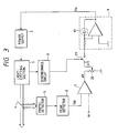
- a pulsed light source of this embodiment similarly includes a light-emitting section (laser) 1 which outputs light in a pulse form in response to supply of a power from a high voltage power supply 2.
- a portion of the output light of the light-emitting section 1 is derived through a beam splitter 4 and received by means of a photodetector 5.
- the photodetector 5 generates an electric signal corresponding to the energy of the reception light and outputs it to a peak detector 8.
- the output of the peak detector 8 is supplied to a comparator 7 which compares the output voltage of the peak detector 8 with a predetermined reference value Vr so as to generate a difference signal ⁇ V in accordance with the comparison result, i.e., in correspondance with the difference therebetween.
- the gain of the comparator 7 is controlled by the variation-measuring circuit 30, which is connected to the photodetector 5.
- the output signal of the comparator 7 is led to a divider 20 so as to regulate the difference signal ⁇ V to a small signal ⁇ s which is proportional thereto.
- the output signal ⁇ s of the divider 20 is led to an analog-to-digital (A/D) converter 11 the output of which is supplied to an adder 12 so as to take the sum of the output of the A/D converter 11 and a voltage [V0] for setting the output of the power supply 2.
- A/D analog-to-digital
- the sum signal is led to a latch 13.
- the voltage [V0] is a digital voltage obtained by the analog-to-digital conversion of the voltage V0.
- the output of the latch 13 is supplied to a digital-to-analog converter (D/A) 14 so as to become an output setting voltage V0.
- D/A digital-to-analog converter
- the pulse energy P starts to decrease while the light-emitting section 1 continuously operates to emits light in a pulse form.
- the photodetector 5 In response to a portion of the output light of the light-emitting section 1, the photodetector 5 generates a voltage signal proportional to the energy of the reception light therefrom.
- the voltage signal is compared with the reference voltage Vr which is a direct-current voltage signal, a great error occurs during a time in which the light-emitting section 1 does not emit the light.
- the peak detector 8 holds the voltage proportional to the reception pulse energy of the photodetector 5 until the next pulse emission of the light-emitting section 1 and produces a direct-current signal Vdc corresponding thereto.
- the gain of the comparator 7 is variable and, in accordance with the output of a variation measuring circuit 30, the gain is set to be small when the variation of the output pulse energy of the light-emitting section 1 is great and on the other hand the gain is set to be great when the variation thereof is small.
- the divider 20 divides the difference signal ⁇ V so as to produce the small signal ⁇ s.
- the small signal ⁇ s is converted in the A/D converter 11 into a digital signal and then added to the previous output setting voltage [V0] so as to produce a signal [V0] + [ ⁇ s] which is in turn supplied to the latch 13.
- the latch 13 rewrites the contents from [V0] to [V0] + [ ⁇ s] at every emission, whereby the output voltage of the power supply 2 is regulated in accordance with the deviation of the previous emission energy at the time of the next emission.
- the synchronous circuit (trigger circuit) 3 supplies the A/D converter 11 with a delay signal s1 synchronous with the termination of the emission and further supplies the latch 13 with a delay signal s2 synchronous with the termination of the analog-to-digital conversion, so that a timing is made so as to reflect a deviation signal to the next output setting voltage V0.
- the light-emitting section 1 is a pulsed laser such as an excimer laser
- the energy of the output light varies at every emission.
- the divider 20 and the variation measuring circuit 30 is for the purpose of no amplification of the variation under the energy control. That is, let it be assumed that the comparator 7 requires that the output voltage of the power supply 2 is increased by ⁇ V1 at the time of the next emission.
- the output of the light-emitting section 1 fluctuates, even if the output voltage of the power supply 2 is increased by ⁇ V1, the output energy does not necessarily become a predetermined value.
- the increase of the output voltage of the power supply 2 rather causes the output fluctuation to become greater.
- the character n is a number below 1 and is set to be small when the output energy variation is great and set to be great when the output energy variation is small, thereby allowing the effect that the output energy can be kept constant without increasing the fluctuation of the output energy.
- emissions whose number is several times to several 10 times are required to return the output energy to a predetermined value.
- a pulsed laser such as an excimer laser
- the output returns to the predetermined value within about 1 second, and the time required therefor is independent on the output variation.
- the A/D converter 11 functions so as to keep the pulse energy constant irrespective of variation of the emission period of the light-emitting section 1. That is, the adder 12 adds the samll signal ⁇ s to the output setting voltage V0 only one time at every emission in response to the delay signal s2, whereby the controlled amount of the output voltage of the power supply 2 becomes constant irrespective of the emission period. Further, in cases where the output setting voltage V0 is held in an analog form by means of a capacitor or the like, when the emission is stopped for a long time, the voltage V0 decreases due to discharging of the capacitor and hence it beomes impossible to obtain a desirable pulse energy at the time of re-start of the emission.
- the output setting voltage V0 is digitized and then held in the latch 13, it is possible to keep the output voltage of the power supply 2 to the previous set value irrespective of the long-time emission stop. Namely, the pulse energy at the time of the re-start of the emission takes a desirable value.
- the peak value of the pulse strength is held, it is also appropriate to hold the integrated value of the pulse waveform. Further, it is appropriate to use a sample and hold circuit, which is a general IC circuit, instead of the peak detector 8.
- the divider 20 is not necessarily provided independently, and it is also appropriate to reduce the gain of the peack detector 8 or the comparator 7.
- the synchronous circuit 3 is not limited to the description. it is also appropriate to detect the emission in conjunction with the power supply 2, the light-emitting section 1 and the photodetector 5 so as to produce the delay signals s1 and s2.
- the pulsed light source can keep the pulse strength constant irrespective of the emission period, the emission stoppage and others.
Landscapes
- Physics & Mathematics (AREA)
- Engineering & Computer Science (AREA)
- Electromagnetism (AREA)
- Optics & Photonics (AREA)
- Plasma & Fusion (AREA)
- Mechanical Engineering (AREA)
- Lasers (AREA)
Applications Claiming Priority (2)
| Application Number | Priority Date | Filing Date | Title |
|---|---|---|---|
| JP77853/90U | 1990-03-27 | ||
| JP2077853A JPH03276782A (ja) | 1990-03-27 | 1990-03-27 | パルス光源 |
Publications (3)
| Publication Number | Publication Date |
|---|---|
| EP0448776A2 true EP0448776A2 (de) | 1991-10-02 |
| EP0448776A3 EP0448776A3 (en) | 1992-05-06 |
| EP0448776B1 EP0448776B1 (de) | 1995-02-01 |
Family
ID=13645622
Family Applications (1)
| Application Number | Title | Priority Date | Filing Date |
|---|---|---|---|
| EP90117953A Expired - Lifetime EP0448776B1 (de) | 1990-03-27 | 1990-09-18 | Regelungssystem für die Ausgangsenergie einer Pulslichtquelle |
Country Status (5)
| Country | Link |
|---|---|
| US (1) | US5134273A (de) |
| EP (1) | EP0448776B1 (de) |
| JP (1) | JPH03276782A (de) |
| CA (1) | CA2025579C (de) |
| DE (1) | DE69016641T2 (de) |
Cited By (3)
| Publication number | Priority date | Publication date | Assignee | Title |
|---|---|---|---|---|
| EP0959395A1 (de) * | 1998-05-22 | 1999-11-24 | TEMIC Semiconductor GmbH | Verfahren zur Regelung einer Regelgrösse |
| EP0866529A3 (de) * | 1997-03-19 | 2000-10-18 | Miyachi Technos Corporation | Eine Lasermonitorvorrichtung und eine Laservorrichtung |
| EP1372515A4 (de) * | 2001-03-26 | 2006-02-01 | Leon C Lahaye | Verfahren und gerät zur überwachung von laseroperationen |
Families Citing this family (16)
| Publication number | Priority date | Publication date | Assignee | Title |
|---|---|---|---|---|
| US5250797A (en) * | 1990-10-05 | 1993-10-05 | Canon Kabushiki Kaisha | Exposure method and apparatus for controlling light pulse emission using determined exposure quantities and control parameters |
| JPH07151701A (ja) * | 1993-11-29 | 1995-06-16 | Hajime Sangyo Kk | ストロボスコープの光量補正機能を有する検査装置 |
| US5523543A (en) * | 1994-09-09 | 1996-06-04 | Litel Instruments | Laser ablation control system and method |
| US5497001A (en) * | 1994-09-15 | 1996-03-05 | Dittler Brothers Incorporated | Flash tube devices |
| US5455837A (en) * | 1994-09-22 | 1995-10-03 | Coherent, Inc. | Flashlamp energy control circuit |
| US5609780A (en) * | 1994-11-14 | 1997-03-11 | International Business Machines, Corporation | Laser system |
| US5834750A (en) * | 1995-02-28 | 1998-11-10 | Psc, Inc. | Bar code scanning system for automatically maintaining constant the amplitude of light reflected from a bar code |
| DE19537467C1 (de) * | 1995-10-07 | 1997-02-27 | Pkl Verpackungssysteme Gmbh | Verfahren und Vorrichtung zum Erzeugen wiederkehrender Muster in kontinuierlich bewegtem Flachmaterial durch Schneiden, Perforieren oder Beschriften mittels Laserbestrahlung |
| JPH10243171A (ja) * | 1997-02-25 | 1998-09-11 | Brother Ind Ltd | 画像読取装置 |
| JP3765044B2 (ja) * | 1998-01-20 | 2006-04-12 | 株式会社小松製作所 | エキシマレーザ装置のエネルギー制御装置 |
| DE19906769A1 (de) * | 1998-02-19 | 1999-12-16 | Leica Microsystems | Überlastschutz zur Vermeidung einer Beschädigung optischer Komponenten |
| US6208370B1 (en) | 1998-12-22 | 2001-03-27 | Eastman Kodak Company | Method and apparatus for determining the starting position and the power of a scanning light beam to be used in writing on a media |
| TWI225190B (en) * | 2003-03-26 | 2004-12-11 | Media Tek Inc | Automatic power controller |
| CN100428103C (zh) * | 2003-04-08 | 2008-10-22 | 联发科技股份有限公司 | 自动功率控制器 |
| US20070201013A1 (en) * | 2006-02-28 | 2007-08-30 | Asml Netherlands B.V. | Lithographic apparatus, device manufacturing method and energy sensor |
| US7868999B2 (en) | 2006-08-10 | 2011-01-11 | Asml Netherlands B.V. | Lithographic apparatus, source, source controller and control method |
Family Cites Families (11)
| Publication number | Priority date | Publication date | Assignee | Title |
|---|---|---|---|---|
| US4611270A (en) * | 1983-09-16 | 1986-09-09 | Questek Incorporated | Method and means of controlling the output of a pulsed laser |
| JPH0821173B2 (ja) * | 1984-07-27 | 1996-03-04 | 松下電器産業株式会社 | 半導体レ−ザ駆動回路 |
| JPS6190540A (ja) * | 1984-10-09 | 1986-05-08 | Olympus Optical Co Ltd | 光出力安定化装置 |
| JPS6269577A (ja) * | 1985-09-21 | 1987-03-30 | Ushio Inc | パルス放電型レ−ザの出力制御装置 |
| US4837787A (en) * | 1986-06-04 | 1989-06-06 | Konishiroku Photo Industry Co., Ltd. | Semiconductor laser device with light emission inhibiting means |
| JPH0621878B2 (ja) * | 1986-07-21 | 1994-03-23 | 株式会社日立製作所 | 異物検査方法 |
| JP2548930B2 (ja) * | 1987-02-16 | 1996-10-30 | 旭光学工業株式会社 | 半導体レ−ザの光出力制御装置 |
| JPH0618422B2 (ja) * | 1987-10-20 | 1994-03-09 | 富士写真フイルム株式会社 | レーザ記録装置 |
| JPH01135082A (ja) * | 1987-11-20 | 1989-05-26 | Ricoh Co Ltd | 半導体レーザ制御装置 |
| US5026978A (en) * | 1989-01-25 | 1991-06-25 | Omron Corporation | Photoelectric switch having pulse driver circuitry |
| JPH0399484A (ja) * | 1989-09-12 | 1991-04-24 | Brother Ind Ltd | 半導体レーザ駆動回路 |
-
1990
- 1990-03-27 JP JP2077853A patent/JPH03276782A/ja active Pending
- 1990-09-18 US US07/583,940 patent/US5134273A/en not_active Expired - Lifetime
- 1990-09-18 EP EP90117953A patent/EP0448776B1/de not_active Expired - Lifetime
- 1990-09-18 CA CA002025579A patent/CA2025579C/en not_active Expired - Fee Related
- 1990-09-18 DE DE69016641T patent/DE69016641T2/de not_active Expired - Fee Related
Cited By (4)
| Publication number | Priority date | Publication date | Assignee | Title |
|---|---|---|---|---|
| EP0866529A3 (de) * | 1997-03-19 | 2000-10-18 | Miyachi Technos Corporation | Eine Lasermonitorvorrichtung und eine Laservorrichtung |
| EP0959395A1 (de) * | 1998-05-22 | 1999-11-24 | TEMIC Semiconductor GmbH | Verfahren zur Regelung einer Regelgrösse |
| US6166597A (en) * | 1998-05-22 | 2000-12-26 | Temic Semiconductor Gmbh | Method for feedback control of a controlled variable |
| EP1372515A4 (de) * | 2001-03-26 | 2006-02-01 | Leon C Lahaye | Verfahren und gerät zur überwachung von laseroperationen |
Also Published As
| Publication number | Publication date |
|---|---|
| CA2025579C (en) | 1994-04-12 |
| DE69016641D1 (de) | 1995-03-16 |
| DE69016641T2 (de) | 1995-05-24 |
| CA2025579A1 (en) | 1991-09-28 |
| US5134273A (en) | 1992-07-28 |
| JPH03276782A (ja) | 1991-12-06 |
| EP0448776A3 (en) | 1992-05-06 |
| EP0448776B1 (de) | 1995-02-01 |
Similar Documents
| Publication | Publication Date | Title |
|---|---|---|
| US5134273A (en) | Control of output energy of a pulsed light source comprising a gas discharge laser | |
| US5724170A (en) | Automatic power control circuit | |
| US4166985A (en) | Injection laser stabilization | |
| CA2618526C (en) | Fiber pulse laser apparatus and method of control the same | |
| US6330258B1 (en) | Laser apparatus | |
| US6038240A (en) | Method and solid-state laser system for generating laser pulses with a variable pulse repetition frequency and constant beam characteristics | |
| GB1272726A (en) | Servo aided injection phase-locked laser oscillator | |
| JPH08114528A (ja) | 光増幅器雑音指数測定方法および装置 | |
| JP2647832B2 (ja) | レーザ発振器 | |
| JP3879889B2 (ja) | インジェクションロック型狭帯域化パルスレーザ装置 | |
| US4627063A (en) | Laser oscillator | |
| WO2020235222A1 (ja) | 受動qスイッチレーザ装置、制御方法、及びレーザ加工装置 | |
| KR102615048B1 (ko) | 레이저가공기 및 그 전원장치 | |
| Araki et al. | An ultraviolet nanosecond light pulse generator using a light emitting diode for test of photodetectors | |
| US5787103A (en) | Operating and control system for lasers useful in bar code scanners | |
| JPH0740615B2 (ja) | パルスレ−ザ発振器 | |
| US4787087A (en) | Circuit for driving a laser diode | |
| US6449297B1 (en) | Power supply unit for solid-state laser, solid state laser, and laser beam generator | |
| JP2002359422A (ja) | Qスイッチレーザ制御装置およびレーザ装置 | |
| US4866721A (en) | Pulsed laser stabilizing device | |
| GB2204442A (en) | Power supply for radio-frequency excited gas laser | |
| JPH0316287A (ja) | パルス光源 | |
| CN119695624B (zh) | 高精度单频激光种子注入锁定方法 | |
| JP5303305B2 (ja) | レーザ制御装置 | |
| JPH02246287A (ja) | パルス光源 |
Legal Events
| Date | Code | Title | Description |
|---|---|---|---|
| PUAI | Public reference made under article 153(3) epc to a published international application that has entered the european phase |
Free format text: ORIGINAL CODE: 0009012 |
|
| 17P | Request for examination filed |
Effective date: 19900918 |
|
| AK | Designated contracting states |
Kind code of ref document: A2 Designated state(s): DE FR GB |
|
| PUAL | Search report despatched |
Free format text: ORIGINAL CODE: 0009013 |
|
| AK | Designated contracting states |
Kind code of ref document: A3 Designated state(s): DE FR GB |
|
| 17Q | First examination report despatched |
Effective date: 19930929 |
|
| GRAA | (expected) grant |
Free format text: ORIGINAL CODE: 0009210 |
|
| AK | Designated contracting states |
Kind code of ref document: B1 Designated state(s): DE FR GB |
|
| PG25 | Lapsed in a contracting state [announced via postgrant information from national office to epo] |
Ref country code: FR Effective date: 19950201 |
|
| REF | Corresponds to: |
Ref document number: 69016641 Country of ref document: DE Date of ref document: 19950316 |
|
| EN | Fr: translation not filed | ||
| PLBE | No opposition filed within time limit |
Free format text: ORIGINAL CODE: 0009261 |
|
| STAA | Information on the status of an ep patent application or granted ep patent |
Free format text: STATUS: NO OPPOSITION FILED WITHIN TIME LIMIT |
|
| 26N | No opposition filed | ||
| PGFP | Annual fee paid to national office [announced via postgrant information from national office to epo] |
Ref country code: GB Payment date: 20010919 Year of fee payment: 12 |
|
| PGFP | Annual fee paid to national office [announced via postgrant information from national office to epo] |
Ref country code: DE Payment date: 20011001 Year of fee payment: 12 |
|
| REG | Reference to a national code |
Ref country code: GB Ref legal event code: IF02 |
|
| PG25 | Lapsed in a contracting state [announced via postgrant information from national office to epo] |
Ref country code: GB Free format text: LAPSE BECAUSE OF NON-PAYMENT OF DUE FEES Effective date: 20020918 |
|
| PG25 | Lapsed in a contracting state [announced via postgrant information from national office to epo] |
Ref country code: DE Free format text: LAPSE BECAUSE OF NON-PAYMENT OF DUE FEES Effective date: 20030401 |
|
| GBPC | Gb: european patent ceased through non-payment of renewal fee |
Effective date: 20020918 |