EP0448919B1 - Support d'enregistrement - Google Patents
Support d'enregistrement Download PDFInfo
- Publication number
- EP0448919B1 EP0448919B1 EP90850411A EP90850411A EP0448919B1 EP 0448919 B1 EP0448919 B1 EP 0448919B1 EP 90850411 A EP90850411 A EP 90850411A EP 90850411 A EP90850411 A EP 90850411A EP 0448919 B1 EP0448919 B1 EP 0448919B1
- Authority
- EP
- European Patent Office
- Prior art keywords
- layer
- medium
- recording
- layers
- magneto
- Prior art date
- Legal status (The legal status is an assumption and is not a legal conclusion. Google has not performed a legal analysis and makes no representation as to the accuracy of the status listed.)
- Expired - Lifetime
Links
- 239000000758 substrate Substances 0.000 claims description 14
- 238000004544 sputter deposition Methods 0.000 claims description 9
- 229910052581 Si3N4 Inorganic materials 0.000 claims description 6
- HQVNEWCFYHHQES-UHFFFAOYSA-N silicon nitride Chemical compound N12[Si]34N5[Si]62N3[Si]51N64 HQVNEWCFYHHQES-UHFFFAOYSA-N 0.000 claims description 6
- FOPBMNGISYSNED-UHFFFAOYSA-N [Fe].[Co].[Tb] Chemical compound [Fe].[Co].[Tb] FOPBMNGISYSNED-UHFFFAOYSA-N 0.000 claims description 3
- RVTZCBVAJQQJTK-UHFFFAOYSA-N oxygen(2-);zirconium(4+) Chemical compound [O-2].[O-2].[Zr+4] RVTZCBVAJQQJTK-UHFFFAOYSA-N 0.000 claims description 2
- 229910003451 terbium oxide Inorganic materials 0.000 claims description 2
- SCRZPWWVSXWCMC-UHFFFAOYSA-N terbium(iii) oxide Chemical compound [O-2].[O-2].[O-2].[Tb+3].[Tb+3] SCRZPWWVSXWCMC-UHFFFAOYSA-N 0.000 claims description 2
- 229910001928 zirconium oxide Inorganic materials 0.000 claims description 2
- 229910017083 AlN Inorganic materials 0.000 claims 1
- PIGFYZPCRLYGLF-UHFFFAOYSA-N Aluminum nitride Chemical compound [Al]#N PIGFYZPCRLYGLF-UHFFFAOYSA-N 0.000 claims 1
- 238000004519 manufacturing process Methods 0.000 claims 1
- 239000010410 layer Substances 0.000 description 68
- 230000007704 transition Effects 0.000 description 12
- 230000005381 magnetic domain Effects 0.000 description 5
- 239000000463 material Substances 0.000 description 4
- 230000006872 improvement Effects 0.000 description 3
- 238000000034 method Methods 0.000 description 3
- 230000003287 optical effect Effects 0.000 description 3
- 230000008569 process Effects 0.000 description 3
- 229910052782 aluminium Inorganic materials 0.000 description 2
- XAGFODPZIPBFFR-UHFFFAOYSA-N aluminium Chemical compound [Al] XAGFODPZIPBFFR-UHFFFAOYSA-N 0.000 description 2
- 239000011521 glass Substances 0.000 description 2
- 238000012935 Averaging Methods 0.000 description 1
- RYGMFSIKBFXOCR-UHFFFAOYSA-N Copper Chemical compound [Cu] RYGMFSIKBFXOCR-UHFFFAOYSA-N 0.000 description 1
- 230000005374 Kerr effect Effects 0.000 description 1
- 229910045601 alloy Inorganic materials 0.000 description 1
- 239000000956 alloy Substances 0.000 description 1
- 229910052802 copper Inorganic materials 0.000 description 1
- 239000010949 copper Substances 0.000 description 1
- PMHQVHHXPFUNSP-UHFFFAOYSA-M copper(1+);methylsulfanylmethane;bromide Chemical compound Br[Cu].CSC PMHQVHHXPFUNSP-UHFFFAOYSA-M 0.000 description 1
- 239000003989 dielectric material Substances 0.000 description 1
- 230000003993 interaction Effects 0.000 description 1
- 230000031700 light absorption Effects 0.000 description 1
- 239000000382 optic material Substances 0.000 description 1
- 229920003023 plastic Polymers 0.000 description 1
- 230000010287 polarization Effects 0.000 description 1
- 239000004417 polycarbonate Substances 0.000 description 1
- 229920000515 polycarbonate Polymers 0.000 description 1
- 229910052761 rare earth metal Inorganic materials 0.000 description 1
- 150000002910 rare earth metals Chemical class 0.000 description 1
- 230000009467 reduction Effects 0.000 description 1
- 239000002356 single layer Substances 0.000 description 1
- 229910052723 transition metal Inorganic materials 0.000 description 1
- 150000003624 transition metals Chemical class 0.000 description 1
- 239000012780 transparent material Substances 0.000 description 1
Images
Classifications
-
- G—PHYSICS
- G11—INFORMATION STORAGE
- G11B—INFORMATION STORAGE BASED ON RELATIVE MOVEMENT BETWEEN RECORD CARRIER AND TRANSDUCER
- G11B11/00—Recording on or reproducing from the same record carrier wherein for these two operations the methods are covered by different main groups of groups G11B3/00 - G11B7/00 or by different subgroups of group G11B9/00; Record carriers therefor
- G11B11/10—Recording on or reproducing from the same record carrier wherein for these two operations the methods are covered by different main groups of groups G11B3/00 - G11B7/00 or by different subgroups of group G11B9/00; Record carriers therefor using recording by magnetic means or other means for magnetisation or demagnetisation of a record carrier, e.g. light induced spin magnetisation; Demagnetisation by thermal or stress means in the presence or not of an orienting magnetic field
- G11B11/105—Recording on or reproducing from the same record carrier wherein for these two operations the methods are covered by different main groups of groups G11B3/00 - G11B7/00 or by different subgroups of group G11B9/00; Record carriers therefor using recording by magnetic means or other means for magnetisation or demagnetisation of a record carrier, e.g. light induced spin magnetisation; Demagnetisation by thermal or stress means in the presence or not of an orienting magnetic field using a beam of light or a magnetic field for recording by change of magnetisation and a beam of light for reproducing, i.e. magneto-optical, e.g. light-induced thermomagnetic recording, spin magnetisation recording, Kerr or Faraday effect reproducing
- G11B11/10582—Record carriers characterised by the selection of the material or by the structure or form
- G11B11/10584—Record carriers characterised by the selection of the material or by the structure or form characterised by the form, e.g. comprising mechanical protection elements
-
- G—PHYSICS
- G11—INFORMATION STORAGE
- G11B—INFORMATION STORAGE BASED ON RELATIVE MOVEMENT BETWEEN RECORD CARRIER AND TRANSDUCER
- G11B11/00—Recording on or reproducing from the same record carrier wherein for these two operations the methods are covered by different main groups of groups G11B3/00 - G11B7/00 or by different subgroups of group G11B9/00; Record carriers therefor
- G11B11/10—Recording on or reproducing from the same record carrier wherein for these two operations the methods are covered by different main groups of groups G11B3/00 - G11B7/00 or by different subgroups of group G11B9/00; Record carriers therefor using recording by magnetic means or other means for magnetisation or demagnetisation of a record carrier, e.g. light induced spin magnetisation; Demagnetisation by thermal or stress means in the presence or not of an orienting magnetic field
- G11B11/105—Recording on or reproducing from the same record carrier wherein for these two operations the methods are covered by different main groups of groups G11B3/00 - G11B7/00 or by different subgroups of group G11B9/00; Record carriers therefor using recording by magnetic means or other means for magnetisation or demagnetisation of a record carrier, e.g. light induced spin magnetisation; Demagnetisation by thermal or stress means in the presence or not of an orienting magnetic field using a beam of light or a magnetic field for recording by change of magnetisation and a beam of light for reproducing, i.e. magneto-optical, e.g. light-induced thermomagnetic recording, spin magnetisation recording, Kerr or Faraday effect reproducing
- G11B11/10582—Record carriers characterised by the selection of the material or by the structure or form
- G11B11/10586—Record carriers characterised by the selection of the material or by the structure or form characterised by the selection of the material
- G11B11/10589—Details
-
- Y—GENERAL TAGGING OF NEW TECHNOLOGICAL DEVELOPMENTS; GENERAL TAGGING OF CROSS-SECTIONAL TECHNOLOGIES SPANNING OVER SEVERAL SECTIONS OF THE IPC; TECHNICAL SUBJECTS COVERED BY FORMER USPC CROSS-REFERENCE ART COLLECTIONS [XRACs] AND DIGESTS
- Y10—TECHNICAL SUBJECTS COVERED BY FORMER USPC
- Y10T—TECHNICAL SUBJECTS COVERED BY FORMER US CLASSIFICATION
- Y10T428/00—Stock material or miscellaneous articles
- Y10T428/26—Web or sheet containing structurally defined element or component, the element or component having a specified physical dimension
- Y10T428/263—Coating layer not in excess of 5 mils thick or equivalent
- Y10T428/264—Up to 3 mils
- Y10T428/265—1 mil or less
Definitions
- This invention relates generally to recording media and relates more particularly to optical recording media having a plurality of thin recording layers.
- Magneto-optic recording disks provide for erasable storage of data.
- the magneto-optic medium typically comprises a transparent substrate, a first transparent dielectric layer, a magneto-optic recording layer, a second transparent dielectric layer and a reflector layer.
- a laser beam is focussed on to a spot on the medium and heats up the magneto-optic material to a temperature at which the magnetic domain of the recording layer is changed.
- a magnetic field is switched in one of two directions to orient the magnetic domain of the spot in either an upward or downward direction.
- the disk is read by focussing a low power laser beam on to the magneto-optic layer.
- the Kerr effect will cause the reflected beam's plane of polarization to be rotated either clockwise or counter-clockwise depending upon whether the spot has an upward or downward magnetic orientation.
- the difference in the rotation is detected and represents either a one or zero.
- a magneto-optic recording medium is comprised of a substrate, a first transparent nonmagnetic layer, a recording section, a second transparent nonmagnetic layer and a reflector layer.
- the recording section comprises a plurality of thin magneto-optic recording layers interspersed with separating thin transparent nonmagnetic layers.
- the multiple magneto-optic layers act to average out the transition jitters in the recorded disk. The result is a medium with a greatly improved signal to noise ratio.
- Fig. 1 is a schematic cross-sectional view of a magneto-optic medium of the prior art and is designated by the general reference number 10.
- Medium 10 has a transparent substrate layer 12.
- a transparent dielectric layer 14 is located below the substrate 12.
- a single magneto-optic recording layer 16 is located below the dielectric layer 14.
- a second transparent dielectric layer 18 is located below the recording layer 16.
- a reflector layer 20 is located below the dielectric layer 18.
- Fig. 2 is a schematic cross-sectional view of a recording medium of the present invention and is designated by the general reference number 50.
- Medium 50 has a transparent substrate 52.
- Substrate 52 may be glass or transparent plastics, such as polycarbonate and is approximately 1.2 mm in thickness.
- the substrate 52 has an index of refraction of approximately 1.5.
- a transparent nonmagnetic layer 54 is located below substrate 52.
- Layer 54 is made of an optically transparent material with low light absorption. The index of refraction is approximately 1.7 or higher. A number of materials may be used in layer 54 including such dielectric materials as silicon nitride, aluminum nitride, zirconium oxide or terbium oxide. The thickness of layer 54 is determined by the index of refraction of the material used in layer 54 and the optical enhancement desired.
- Recording section 56 is located below layer 54.
- Recording section 56 is comprised of a plurality of thin magneto-optic recording layers 60 interspersed with a plurality of thin separating transparent nonmagnetic layers 62. If there are N number of recording layers 60, then there will be (N-1) number of separating layers 62 interspersed between them.
- Magneto-optic recording layers 60 may be made of rare earth and transition metal alloys such as terbium iron cobalt.
- the layers 62 may be made of the same type of material as layer 54.
- the sum of the thicknesses of all recording layers 60 in section 56 is approximately 15 to 40 nm (150 to 400 Angstroms) thick and this sum is about the same thickness as the single recording layer 16 of the prior art.
- a transparent nonmagnetic layer 70 is located below section 56.
- Layer 70 may be made of the same type of material as layer 54.
- a reflector 72 is located below layer 70. Reflector 72 may be made of aluminum or copper. The thickness of layer 70 may be chosen according to the desired optical enhancement.
- Medium 50 is manufactured by a sputtering process. Each layer is deposited in succession on the substrate in a separate sputtering process.
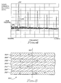
- Fig. 3 shows a schematic cross-sectional view of an embodiment of the recording medium of the present invention and is designated by the general reference number 100.
- Medium 100 has a substrate 102 of 1.2 mm thickness and made of glass.
- a first transparent nonmagnetic layer 104 is located below substrate 102.
- Layer 104 is made of silicon nitride and is approximately 80nm (800 Angstroms) thick.
- a recording section 106 is located below layer 104.
- Section 106 is comprised of a pair of magneto-optic layers 110 interspersed by a single transparent nonmagnetic layer 112.
- Layers 110 are both made of terbium iron cobalt and are each 10 nm (100 Angstroms) thick.
- Layer 112 is made of silicon nitride and is 10nm (100 Angstroms) thick.
- a transparent nonmagnetic layer 120 is located below section 106.
- Layer 120 is made of silicon nitride and is 20 nm (200 Angstroms) thick.
- a reflector layer 122 is located below layer 120 and is made of aluminum.
- Medium 100 is manufactured in a sputtering process similar to that used for medium 50.
- Fig. 4 shows a graph of signal strength and noise versus frequency for reading the medium 100 of Fig. 3.
- a line 200 represents the noise level of the disk prior to writing.
- a line 210 represents the signal received when reading the disk.
- a peak signal 212 represents the recorded data, while the lower levels 214 of line 210 represent the background noise encountered during reading. It can be seen that a carrier signal to noise ratio (point 212 vs. level 214) of approximately 67 dB is obtained. This compares with at most a 64 dB signal to noise ratio of the prior art.
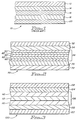
- Fig. 5 shows a schematic cross-sectional view of a recording section 300 of the present invention.
- a plurality of magneto-optic recording layers 302 are interspersed by a plurality of transparent nonmagnetic layers 304.
- a line 310 represents the ideal position of the magnetic domain transition in section 300.
- a plurality of lines 312 represent the actual transition positions in section 300.
- Arrows in layers 302 represent the direction of the magnetic domain on either side of transitions 312. In this case the layers 302 on the left have a downward magnetic direction and the layers 302 on the right have an upward magnetic direction.
- the layers 304 are made thick enough so that there is no exchange interaction between the layers 302. This means that the written magnetic transitions in the recording layers 302 are almost independent of each other.
- the read back transition jitter (i.e. the standard deviation of read back transitions from the ideal average transition) is reduced from that of a single layer by a factor of ⁇ N simply by averaging the transition positions of N magneto-optic recording layers that can be reached by the read beam.
- the media transitions noise will be reduced by 20 log ⁇ N (dB).
- N the expected reduction in jitter noise should be 3 dB. This agrees well with the actual results of Fig. 4 where N equals 2 and the improvement of the carrier signal to noise ratio was approximately 3 dB (from 64 dB to 67 dB).
- the signal to noise ratio can be improved even further by adding more magneto-optic layers.
- the only limitation is that the total thickness of the magneto-optic layers must be small enough to allow the read beam to fully penetrate to the lowest magneto-optic layer. Generally, this means keeping the sum of the thicknesses in the recording layers in the recording section 56 at approximately the same thickness as the single recording layer 16 of the prior art.
- the present invention thus achieves a significant improvement in signal to noise ratio. This improvement will allow the medium to be used at a faster data transfer rate and/or increased recording density.
Claims (8)
- Milieu d'enregistrement magnéto-optique comprenant :un substrat essentiellement transparent (52);une première couche amagnétique essentiellement transparente (54) formée sur le substrat;une section d'enregistrement (56) formée sur la première couche amagnétique, ladite section d'enregistrement comprenant une pluralité de N couches d'enregistrement de données magnéto-optiques (60) entrecalées avec N-1 couches de séparation amagnétiques essentiellement transparentes (62);une deuxième couche amagnétique essentiellement transparente (70) formée sur la section d'enregistrement; etun réflecteur (72) formé sur la deuxième couche amagnétique.
- Milieu selon la revendication 1, où l'épaisseur totale de l'ensemble des dites couches d'enregistrement de données dans la section d'enregistrement est inférieure ou égale à 40 nm (400 Angströms).
- Milieu selon la revendication 1 ou 2, où les couches d'enregistrement de données sont à base de ferrocobalt de terbium.
- Milieu selon la revendication 1, où la couche de séparation est à base de nitrure de silicium.
- Milieu selon la revendication 1, où la première couche amagnétique, les couches de séparation et la deuxième couche amagnétique sont à base de nitrure de silicium.
- Milieu selon la revendication 1, où la couche de séparation est à base de nitrure d'aluminium, d'oxyde de zirconium ou d'oxyde de terbium.
- Milieu selon la revendication 1, où N = 2, chacune des deux couches d'enregistrement et l'unique couche de séparation ayant une épaisseur de 10 nm.
- Procédé de fabrication d'un milieu d'enregistrement magnéto-optique comprenant les étapes consistant à :déposer par pulvérisation cathodique une couche amagnétique essentiellement transparente sur un substrat essentiellement transparent;déposer par pulvérisation cathodique une première couche d'enregistrement de données sur ladite première couche amagnétique;déposer par pulvérisation cathodique une deuxième couche amagnétique essentiellement transparente sur ladite première couche d'enregistrement de données;déposer par pulvérisation cathodique une deuxième couche d'enregistrement de données sur ladite deuxième couche amagnétique;déposer par pulvérisation cathodique une troisième couche amagnétique essentiellement transparente sur ladite deuxième couche d'enregistrement de données; etdéposer par pulvérisation cathodique une couche réfléchissante sur ladite troisième couche amagnétique.
Applications Claiming Priority (2)
| Application Number | Priority Date | Filing Date | Title |
|---|---|---|---|
| US49986090A | 1990-03-26 | 1990-03-26 | |
| US499860 | 1990-03-26 |
Publications (3)
| Publication Number | Publication Date |
|---|---|
| EP0448919A2 EP0448919A2 (fr) | 1991-10-02 |
| EP0448919A3 EP0448919A3 (en) | 1992-03-11 |
| EP0448919B1 true EP0448919B1 (fr) | 1996-02-14 |
Family
ID=23987044
Family Applications (1)
| Application Number | Title | Priority Date | Filing Date |
|---|---|---|---|
| EP90850411A Expired - Lifetime EP0448919B1 (fr) | 1990-03-26 | 1990-12-17 | Support d'enregistrement |
Country Status (4)
| Country | Link |
|---|---|
| US (1) | US5731076A (fr) |
| EP (1) | EP0448919B1 (fr) |
| JP (1) | JPH04221446A (fr) |
| DE (1) | DE69025395T2 (fr) |
Families Citing this family (3)
| Publication number | Priority date | Publication date | Assignee | Title |
|---|---|---|---|---|
| US5648163A (en) * | 1994-09-27 | 1997-07-15 | Imation Corp. | Magneto-optic recording medium having magneto-optic film layers separated by yttrium oxide |
| JP3496113B2 (ja) * | 1997-07-02 | 2004-02-09 | 富士通株式会社 | 情報記録媒体、情報記録媒体の再生方法および情報記録媒体の再生装置 |
| US20020192506A1 (en) | 2001-06-04 | 2002-12-19 | International Business Machines Corporation | `Thermal Spring' magnetic recording media for writing using magnetic and thermal gradients |
Family Cites Families (23)
| Publication number | Priority date | Publication date | Assignee | Title |
|---|---|---|---|---|
| US3650601A (en) * | 1970-11-19 | 1972-03-21 | Du Pont | Magneto-optic device having alternate layer film structure |
| US4025379A (en) * | 1973-05-03 | 1977-05-24 | Whetstone Clayton N | Method of making laminated magnetic material |
| ATE34244T1 (de) * | 1982-12-06 | 1988-05-15 | Plasmon Data Systems Nv | Informationsspeicherung und - aufzeichnung. |
| US4569881A (en) * | 1983-05-17 | 1986-02-11 | Minnesota Mining And Manufacturing Company | Multi-layer amorphous magneto optical recording medium |
| US4833043A (en) * | 1983-05-17 | 1989-05-23 | Minnesota Mining And Manufacturing Company | Amorphous magneto optical recording medium |
| JPH0670858B2 (ja) * | 1983-05-25 | 1994-09-07 | ソニー株式会社 | 光磁気記録媒体とその製法 |
| CA1224270A (fr) * | 1983-09-16 | 1987-07-14 | Junji Hirokane | Element-memoire magneto-optique |
| JPS60145525A (ja) * | 1984-01-10 | 1985-08-01 | Canon Inc | 磁気記録媒体 |
| GB8402419D0 (en) | 1984-01-30 | 1984-02-29 | Risebrow H | Mixing/dispensing fluids |
| FR2560419B1 (fr) * | 1984-02-29 | 1986-06-13 | Bull Sa | Milieu d'enregistrement magneto-optique |
| US4939023A (en) * | 1984-08-13 | 1990-07-03 | Canon Kabushiki Kaisha | Opto-magnetic recording medium |
| DE3584945D1 (de) * | 1984-10-30 | 1992-01-30 | Brother Ind Ltd | Magnetooptisches speichermedium und geraet zum schreiben auf und lesen von dem medium. |
| US4801499A (en) * | 1985-01-24 | 1989-01-31 | Seiko Epson Corporation | Optical recording medium |
| JPH0671828B2 (ja) * | 1985-01-25 | 1994-09-14 | 株式会社日立製作所 | 情報記録用薄膜 |
| US4635076A (en) * | 1985-03-14 | 1987-01-06 | Minnesota Mining And Manufacturing Company | Two-sided optical recording medium |
| CA1254385A (fr) * | 1985-07-26 | 1989-05-23 | Noboru Sato | Support d'enregistrement magneto-optique fait d'un stratifie artificiel amorphe comprenant un element de terre rare et un element de metal de transition |
| US4789606A (en) * | 1986-04-17 | 1988-12-06 | Fuji Photo Film Co., Ltd. | Magneto-optical recording medium |
| JPS62264463A (ja) * | 1986-05-12 | 1987-11-17 | Fuji Photo Film Co Ltd | 光磁気記録媒体 |
| JPS6358642A (ja) * | 1986-08-28 | 1988-03-14 | Sony Corp | 光磁気記録媒体 |
| JPH0782674B2 (ja) * | 1986-11-06 | 1995-09-06 | キヤノン株式会社 | 光磁気メモリ用媒体 |
| KR910006659B1 (ko) * | 1987-10-29 | 1991-08-30 | 미쓰이 세끼유 가가꾸 고오교오 가부시끼가이샤 | 자기광학 기록매체 |
| DE3813171A1 (de) * | 1988-04-20 | 1989-11-02 | Hoechst Ag | Informationsaufzeichnungselement |
| EP0341521A1 (fr) * | 1988-05-09 | 1989-11-15 | Siemens Aktiengesellschaft | Milieu d'emmagasinage magnéto-optique |
-
1990
- 1990-12-17 EP EP90850411A patent/EP0448919B1/fr not_active Expired - Lifetime
- 1990-12-17 DE DE69025395T patent/DE69025395T2/de not_active Expired - Fee Related
-
1991
- 1991-02-22 JP JP3048827A patent/JPH04221446A/ja active Pending
-
1993
- 1993-02-11 US US08/017,941 patent/US5731076A/en not_active Expired - Fee Related
Also Published As
| Publication number | Publication date |
|---|---|
| US5731076A (en) | 1998-03-24 |
| EP0448919A3 (en) | 1992-03-11 |
| EP0448919A2 (fr) | 1991-10-02 |
| JPH04221446A (ja) | 1992-08-11 |
| DE69025395T2 (de) | 1996-09-19 |
| DE69025395D1 (de) | 1996-03-28 |
Similar Documents
| Publication | Publication Date | Title |
|---|---|---|
| JP3781823B2 (ja) | 光磁気記録媒体及びその再生方法 | |
| US5087340A (en) | Method of making magneto-optical recording disk | |
| EP0448919B1 (fr) | Support d'enregistrement | |
| US5875169A (en) | Magneto-optic data storage device having multiple data storage levels | |
| US5665467A (en) | Magneto-optical recording medium | |
| EP0475452B1 (fr) | Couche diélectrique quasi-amorphe ou amorphe de bioxide de zirconium pour milieux optiques ou magnéto-optiques de mémoire | |
| Carcia et al. | MATERIALS'CHALLENGES FOR METAL MULTILAYERS AS A MAGNETO-OPTICAL RECORDING MEDIUM | |
| US5612109A (en) | Optical storage medium including multiple data levels made of Co/Pt magneto-optic recording media | |
| JPH076420A (ja) | 光磁気記録媒体 | |
| JP2728503B2 (ja) | 光磁気記録媒体 | |
| EP0239974A2 (fr) | Milieu d'enregistrement magnéto-optique | |
| JP2829335B2 (ja) | 光磁気記録媒体 | |
| JPH0328739B2 (fr) | ||
| EP0515222B1 (fr) | Dispositif de stockage magnétooptique | |
| JP2753583B2 (ja) | 光磁気記録媒体 | |
| KR100205403B1 (ko) | 광자기 기록매체의 구조 | |
| JP2604361B2 (ja) | 光磁気記録媒体 | |
| JP3214513B2 (ja) | 光磁気記録媒体 | |
| JPH09106572A (ja) | 光記録媒体 | |
| KR100587257B1 (ko) | 광자기 디스크 및 그 제조방법 | |
| KR100225108B1 (ko) | 단파장용 광자기 기록 매체 | |
| KR960007904B1 (ko) | 광자기 기록매체 | |
| JP2528088B2 (ja) | 光磁気記録媒体の製造方法及び光磁気記録媒体 | |
| JP2678222B2 (ja) | 光磁気記録媒体 | |
| JPH0337841A (ja) | 光ディスク |
Legal Events
| Date | Code | Title | Description |
|---|---|---|---|
| PUAI | Public reference made under article 153(3) epc to a published international application that has entered the european phase |
Free format text: ORIGINAL CODE: 0009012 |
|
| AK | Designated contracting states |
Kind code of ref document: A2 Designated state(s): DE FR GB |
|
| PUAL | Search report despatched |
Free format text: ORIGINAL CODE: 0009013 |
|
| 17P | Request for examination filed |
Effective date: 19911219 |
|
| AK | Designated contracting states |
Kind code of ref document: A3 Designated state(s): DE FR GB |
|
| 17Q | First examination report despatched |
Effective date: 19940628 |
|
| GRAA | (expected) grant |
Free format text: ORIGINAL CODE: 0009210 |
|
| AK | Designated contracting states |
Kind code of ref document: B1 Designated state(s): DE FR GB |
|
| REF | Corresponds to: |
Ref document number: 69025395 Country of ref document: DE Date of ref document: 19960328 |
|
| ET | Fr: translation filed | ||
| PG25 | Lapsed in a contracting state [announced via postgrant information from national office to epo] |
Ref country code: GB Effective date: 19961217 |
|
| PLBE | No opposition filed within time limit |
Free format text: ORIGINAL CODE: 0009261 |
|
| STAA | Information on the status of an ep patent application or granted ep patent |
Free format text: STATUS: NO OPPOSITION FILED WITHIN TIME LIMIT |
|
| 26N | No opposition filed | ||
| GBPC | Gb: european patent ceased through non-payment of renewal fee |
Effective date: 19961217 |
|
| PG25 | Lapsed in a contracting state [announced via postgrant information from national office to epo] |
Ref country code: FR Effective date: 19970829 |
|
| PG25 | Lapsed in a contracting state [announced via postgrant information from national office to epo] |
Ref country code: DE Effective date: 19970902 |
|
| REG | Reference to a national code |
Ref country code: FR Ref legal event code: ST |