EP0449310B1 - On-Chip-Spannungsregler und Halbleiterspeichervorrichtung mit Verwendung desgleichen - Google Patents
On-Chip-Spannungsregler und Halbleiterspeichervorrichtung mit Verwendung desgleichen Download PDFInfo
- Publication number
- EP0449310B1 EP0449310B1 EP91105071A EP91105071A EP0449310B1 EP 0449310 B1 EP0449310 B1 EP 0449310B1 EP 91105071 A EP91105071 A EP 91105071A EP 91105071 A EP91105071 A EP 91105071A EP 0449310 B1 EP0449310 B1 EP 0449310B1
- Authority
- EP
- European Patent Office
- Prior art keywords
- voltage
- regulator
- gate
- transistor
- chip
- Prior art date
- Legal status (The legal status is an assumption and is not a legal conclusion. Google has not performed a legal analysis and makes no representation as to the accuracy of the status listed.)
- Expired - Lifetime
Links
Images


Classifications
-
- G—PHYSICS
- G11—INFORMATION STORAGE
- G11C—STATIC STORES
- G11C11/00—Digital stores characterised by the use of particular electric or magnetic storage elements; Storage elements therefor
- G11C11/21—Digital stores characterised by the use of particular electric or magnetic storage elements; Storage elements therefor using electric elements
- G11C11/34—Digital stores characterised by the use of particular electric or magnetic storage elements; Storage elements therefor using electric elements using semiconductor devices
- G11C11/40—Digital stores characterised by the use of particular electric or magnetic storage elements; Storage elements therefor using electric elements using semiconductor devices using transistors
- G11C11/401—Digital stores characterised by the use of particular electric or magnetic storage elements; Storage elements therefor using electric elements using semiconductor devices using transistors forming cells needing refreshing or charge regeneration, i.e. dynamic cells
- G11C11/4063—Auxiliary circuits, e.g. for addressing, decoding, driving, writing, sensing or timing
- G11C11/407—Auxiliary circuits, e.g. for addressing, decoding, driving, writing, sensing or timing for memory cells of the field-effect type
-
- G—PHYSICS
- G11—INFORMATION STORAGE
- G11C—STATIC STORES
- G11C5/00—Details of stores covered by group G11C11/00
- G11C5/14—Power supply arrangements, e.g. power down, chip selection or deselection, layout of wirings or power grids, or multiple supply levels
- G11C5/147—Voltage reference generators, voltage or current regulators; Internally lowered supply levels; Compensation for voltage drops
-
- G—PHYSICS
- G05—CONTROLLING; REGULATING
- G05F—SYSTEMS FOR REGULATING ELECTRIC OR MAGNETIC VARIABLES
- G05F1/00—Automatic systems in which deviations of an electric quantity from one or more predetermined values are detected at the output of the system and fed back to a device within the system to restore the detected quantity to its predetermined value or values, i.e. retroactive systems
- G05F1/10—Regulating voltage or current
- G05F1/46—Regulating voltage or current wherein the variable actually regulated by the final control device is DC
- G05F1/462—Regulating voltage or current wherein the variable actually regulated by the final control device is DC as a function of the requirements of the load, e.g. delay, temperature, specific voltage/current characteristic
- G05F1/465—Internal voltage generators for integrated circuits, e.g. step down generators
-
- G—PHYSICS
- G11—INFORMATION STORAGE
- G11C—STATIC STORES
- G11C5/00—Details of stores covered by group G11C11/00
- G11C5/14—Power supply arrangements, e.g. power down, chip selection or deselection, layout of wirings or power grids, or multiple supply levels
Definitions
- the present invention generally relates to semiconductor integrated circuits, and more particularly to an on-chip voltage regulator for controlling the generation of an internal power supply voltage from an external power supply voltage.
- the first approach is to produce a transistor having a gate length of approximately 0.8 micrometers which is enough to withstand a high power supply voltage equal to, for example, 5 volts.
- the second approach is to produce a transistor having a gate length of approximately 0.5 micrometers which is suitable for a decreased power supply voltage equal to, for example, 3.3 volts. It should be noted that the transistor produced by the second approach can operate faster than that produced by the first approach.
- the power supply voltage should be decreased to a suitable voltage as the integration density increases.
- many IC chips are designed to receive a standardized external power supply voltage equal to 5 volts. Thus, it is necessary to generate a suitably dropped power supply voltage from the standardized external power supply voltage inside of each IC chip.
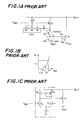
- FIG.1A is a circuit diagram of a conventional on-chip voltage regulator designed to generate, from an external voltage, an in-chip voltage lower than the external voltage.
- a regulator transistor Q1 functions as a series control regulator with respect to an external power supply voltage V EXT equal to, for example, 5 volts.
- the regulator transistor Q1 generates an internal power supply voltage V INT equal to, for example, 3.3 volts from the 5.0V external power supply voltage V EXT .
- the gate of the regulator transistor Q1 is charged by a voltage obtained by rectifying an A.C. signal generated by a ring oscillator OSC.
- the gate voltage now labeled V G1 is clamped at a fixed voltage due to the function of a transistor Q4 because the source of the transistor Q4 is set to a reference voltage V REF .
- the reference voltage V REF can be generated by a conventional method, for example, by using the threshold voltage of a MOS transistor.
- a transistor Q2 functions to charge the gate of the regulator transistor Q1 when the power supply is turned ON.
- the reference voltage V REF is also applied to the gate of the transistor Q2 and the oscillator OSC.
- the reference voltage V REF enables the oscillator OSC to generate a fixed oscillation voltage.
- a capacitor C is connected between the oscillator OSC and the source of the transistor Q2, and functions to increase the charge voltage. For example, when the output voltage of the oscillator OSC is negative, the capacitor C is charged via the transistor Q2 so that the terminal of the C on the side of the transistor Q2 is positive.
- the oscillator OSC when the output voltage of the oscillator OSC is positive, the charge voltage is increased so that it becomes equal to the sum of the positive output voltage of the oscillator OSC and the voltage developed across the capacitor C.
- the oscillator OSC is used for generating the large gate voltage V G1 of the regulator transistor Q1 in order to obtain the stabilized internal voltage V INT .
- the oscillator OSC may be replaced by an alternative device, which oscillates and rectifies a voltage signal so that a peak voltage can be obtained.
- FIG.1B is a drain current (I D ) vs. a gate-source voltage (V GS ) of the regulator transistor Q1.
- the peak of the current passing through the regulator transistor Q1 becomes approximately equal to 100 mA. That is, the current obtained at the active mode is 1000 times the current obtained in the standby mode. It is possible to increase the gate width to increase the proportional constant k. However, an increase in the gate width decreases the integration density. It can be seen from the above explanation that it is impossible to regulate the internal voltage V INT at the fixed voltage in the state where the current consumed in the internal circuit is varying. Further, an increase in the gate width leads to an increase in a sub-threshold current, and the threshold voltage of the transistor Q1 is greatly decreased. Thus, if a change in the current consumed in the internal chip is equal to 1000 times that obtained in the standby mode, it causes great variations in the internal voltage V INT .
- FIG.1C is another conventional on-chip voltage regulator directed to suppressing variations in the internal voltage V INT .
- the gate voltage of the regulator transistor Q1 is controlled by an output of a current-mirror type analog differential amplifier, which is composed of transistors Q11 - Q14. That is, a feedback signal is applied to the gate of the transistor Q12 from the source of the transistor Q1, that is, a node from which the internal voltage V INT is output.
- the reference voltage V REF is applied to the gate of the transistor Q11.
- the internal voltage V INT is automatically controlled so that it is always equal to the reference voltage V REF .
- the internal voltage V INT is not greatly affected by variations in a load current, that is, the drain current of the transistor Q1.
- the on-chip voltage regulator comprises clock receiving means for receiving a predetermined clock signal related to an operation of the internal circuit as well as regulator means coupled to the clock receiving means and the regulator transistor for generating a gate voltage output to the gate of the regulator transistor on the basis of a state of the predetermined clock signal so that the regulator transistor can generate a substantially fixed internal voltage from the external power supply voltage irrespective of whether or not the internal circuit is operating.
- a more specific object of the present invention is to provide an on-chip voltage regulator capable of generating an internal voltage little affected by variations in the load current and consuming a small amount of current in the standby mode.
- an on-chip voltage regulator for controlling a gate of a regulator transistor having a first terminal connectable to receive an external power supply voltage and a second terminal connectable to an internal circuit formed on a chip on which the on-chip voltage regulator is formed
- the on-chip regulator comprising clock receiving means for receiving a predetermined clock signal related to an operation of the internal circuit, and regulator means coupled to the clock receiving means and the regulator transistor for generating a gate voltage output to the gate of the regulator transistor on the basis of a state of the predetermined clock signal so that the regulator transistor can generate a substantially fixed internal voltage from the external power supply voltage irrespective of whether or not the internal circuit is operating, wherein a capacitance is added to the gate of the regulator transistor and the gate potential of the regulator transistor is controlled on the basis of the active period of the clock or its frequency.
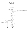
- an on-chip voltage regulator 100 controls the regulator transistor Q1.
- the voltage regulator 100 has an input terminal receiving a clock signal CLK ⁇ , and an output terminal (node N) connected to the gate of the regulator transistor Q1 formed of an n-channel MOS transistor.
- the voltage regulator 100 is composed of a constant-current source I, diode-connected n-channel MOS transistors Q26, Q27, Q28 and Q29 connected in series, an n-channel MOS transistor Q30, and a capacitor C.
- the constant-current source I, and the transistors Q26 - Q29 are connected in series and provided between a positive internal voltage line having a voltage V A and ground.
- the gate of each of the transistors Q26 - Q29 is connected to the drain thereof.
- the transistors Q30 is connected in parallel to the transistor Q29.
- a low-active clock signal CLK ⁇ is applied to the gate of the transistor Q30.
- a corresponding internal circuit illustrated as a load L in FIG.2
- the capacitor C is connected between the node N1 and ground.
- V1 a voltage developed across the series connected transistors Q26 - Q28
- V2 a voltage developed across the transistor Q29.
- the load L (corresponding to an internal circuit) on a chip on which the voltage regulator is also formed is maintained in the standby mode, the low-active clock signal CLK ⁇ is maintained at the high level.
- the transistor Q30 is conducting, the gate voltage of the regulator transistor Q30 is equal to the sum of the threshold voltages Vth of the transistors Q26 - Q28.
- a bias current supplied to the transistors Q26 - Q28 is supplied from the constant-current source I, which make it possible to provide the voltage VI which does not change even if the voltage V A changes. It is preferable that the internal voltage V A be set to be higher than the standardized voltage of the external power supply voltage V EXT when the transistor Q1 is formed of an enhancement type MOS transistor.
- V INT V G1 - V GS
- V GS is a gate-source bias voltage of the regulator transistor Q1 which corresponds to a current consumed in a load L in the standby mode, and is approximately equal to the threshold voltage Vth of the regulator transistor Q1.
- the clock signal CLK ⁇ falls, so that the chip is activated and an internal circuit formed therein starts to operate.
- the amount of power consumed in the internal circuit starts to increase.
- the clock signal CLK ⁇ changes to the low level
- the transistor Q30 is turned OFF.
- the gate voltage V G1 of the regulator transistor Q1 increases by the voltage V2 equal to the threshold voltage Vth of the transistor Q29.
- An increase in the gate voltage V G1 cooperates with a charging operation in which the current generated from the constant-current source I charges a large capacitor including the capacitor C1 and a gate capacitor of the regulator transistor Q1.
- the n increase in the gate voltage V G1 does not occur rapidly.
- the gate voltage V G1 of the regulator transistor Q1 becomes equal to (V1 + V2) at time t3.
- the internal voltage V INT is slightly decreasing.
- the internal voltage V INT is continuously decreasing even after time t2, as depicted by a broken line C2 in FIG.3. This means that a large variation in the internal voltage V INT occurs.
- the transistor Q30 is omitted, the internal voltage V INT will be decreasing continuously after time t2.
- the voltage V2 equal to the threshold voltage Vth of the transistor Q29 is added to the voltage V1, so that the gate voltage V G1 of the regulator transistor Q1 is increased.
- the potential of the node N1 is close to (V1 and V2). If the clock signal CLK ⁇ is maintained at the low level for a long time, the potential of the node N1 becomes equal to (V1 + V2). In other words, the regulator transistor Q1 is controlled so that the internal resistance thereof decreases.
- the gate voltage V G1 of the regulator transistor Q1 is regulated in the above-mentioned way, so that a decrease in the internal voltage V INT is compensated for.
- the internal resistance of the regulator transistor Q1 is controlled on the basis of the ON/OFF frequency (or the activated period) of the clock signal CLK ⁇ .
- the configuration shown in FIG.2 does not use any differential amplifier circuit.
- the internal resistance of the regulator transistor Q1 is changed so that the voltage drop obtained when a small amount of current passes through the internal circuit is substantially equal to the voltage drop obtained when a large amount of current passes through the internal circuit.
- the load L includes a capacitor of a circuit element and/or a parasitic capacitor.
- the internal voltage V INT is associated with the charging and discharging of such a capacitor. Thus, a variation takes place slowly.
- the clock signal CLK ⁇ is frequently switched between the standby mode and the activate mode, the capacitance of the capacitor C and/or a change in the internal resistance of the regulator transistor Q1 are adjusted so that the internal voltage V INT is always substantially fixed.
- An on-chip voltage regulator 100A includes the constant-current source I which is formed of a depletion type n-channel MOS transistor in which its gate and source are short-circuited.
- the regulator transistor Q1 is also formed of a depletion type n-channel MOS transistor in which its gate and source are short-circuited.
- the circuit is designed to pass a large amount of current through the regulator transistor Q1 in a five-tube characteristic region. Such an operation results in a substrate current.
- FIG.4B shows the cross section of a semiconductor chip which realizes the transistor Q1 or Q25 shown in FIG.4A.
- the transistor is formed in a p-type silicon substrate 1, which is biased by a substrate bias voltage V BB (or V SS ) which is generated in the chip.
- V BB substrate bias voltage
- the substrate current flows into a V BB generation circuit (which corresponds to a substrate bias generator, as will be described later), and causes the V BB generation circuit to operate unstably.
- an n-type well 2 is formed in the p-type substrate 1, and a p-type well 3 is formed in the n-type well 2.
- the p-type well 3 is electrically connected to a source region S.
- the transistor Q25 can be fabricated in the same way as the regulator transistor Q1. However, the reason why the transistor Q25 is formed in the p-type well in the n-type well is different from the above-mentioned reason regarding the regulator transistor Q1.
- the transistor Q25 functions as a constant-current source by connecting the gate to the source. Since the constant-current output of the transistor Q25 is output from the source thereof, a change in the source voltage causes a change in a backgate voltage (which corresponds to the potential difference between the source of the transistor Q25 and the potential of the p-type substrate 1 which is the back gate), if the transistor Q25 is directly formed in the p-type substrate 1. Thus, a so-called substrate bias effect appears and deteriorates the constant-current characteristic of the transistor Q25.
- the substrate bias effect is such that as the back gate bias increases, the threshold voltage Vth of the transistor Q25 increases and thus the drain current decreases.
- the layer structure shown in FIG.4B is formed so that the back gate is the p-type well 3 in the n-type well 2, and the p-type well 3 is connected to the source 5.
- the back gate voltage also changes, so that the occurrence of a change in the drain current arising from the substrate bias effect can be suppressed.
- a good constant-current characteristic can be obtained.
- the transistor Q25 is formed of a depletion type MOS transistor, and thus it is not necessary to provide the aforementioned voltage V A higher than the standard external power supply voltage V EXT , as shown in FIG.2. It is necessary to generate the voltage V A higher than the power supply voltage V EXT inside of the chip. Such a V A generation circuit consumes some power. Thus, it is preferable to use the configuration shown in FIG.4A in most cases.
- FIG.4C shows the cross section of an alternative layer structure designed to preventing the occurrence of the aforementioned substrate bias effect.
- a transistor is formed in a p-type well 5 formed in an n-type silicon substrate 4, and the p-type well 5 is electrically connected to the source S.
- the circuit structure for generating and oscillating the gate voltage V G1 of the regulator transistor Q1 is not limited to the aforementioned circuit structure.
- m transistors (m is an integer equal to or larger than 1) and n transistors (n is an integer equal to or larger than 1) are connected in series.
- CLK ⁇ When the clock signal CLK ⁇ is at the low level, a voltage equal to n x Vth is added to a voltage equal to m x Vth.
- the m transistors and n transistors can be replaced by alternative resistance elements, such as diodes.
- FIG.6 shows a DRAM device, which includes a RAS ⁇ (Row Address Strobe) system 200, a CAS ⁇ system (Column Address Strobe) system 300, a sense system 400 and an internal voltage generation circuit 500.
- the RAS ⁇ system 200 operates in accordance with a row address strobe signal RAS ⁇ or a clock synchronized with the RAS ⁇ signal.
- the CAS ⁇ system 300 operates in accordance with a column address strobe signal CAS ⁇ or a clock synchronized with the CAS ⁇ signal.
- the sense system 300 operates in accordance with a pair of sense amplifier driving clocks ⁇ s and ⁇ s .
- the internal voltage generation circuit 500 includes three internal voltage generator 37, 38 and 39.
- the RAS ⁇ system 200 includes a predecoder 12a, a predecoder 12b, a row address decoder 16, a clock generator 18, a mode controller 32 and a refresh address counter 34.
- the CAS ⁇ system 300 includes the address buffer 12a, the predecoder 12b, a column address decoder 14, a clock generator 22, a write clock generator 26 and a data input buffer 28.
- the sense system 300 includes a memory cell array 10, and a sense amplifier/input output gate 24.
- the memory cell array 10 has a plurality of memory cells arranged into rows and columns and coupled to word lines and bit lines.
- a multiplexed address signal ADD consisting of address bits A0 to A10 is input to the address buffer 12a, which outputs a column address signal to the column address decoder 14.
- the address signal ADD is also supplied to the predecoder 12b, which outputs a row address signal to the row address decoder 16.
- the row address strobe signal RAS ⁇ from an external device (not shown), such as a central processing unit (CPU), is input to the clock generator 18, which generates a clock signal supplied to the row address decoder 16.
- the row address strobe signal RAS ⁇ is a low-active signal and defines a timing at which at least one of the word lines is selected by the row address decoder 16, and a timing at which at least selected one of the word lines is released from the selected state.
- the sense amplifier and input/output gate 24 is connected to the column address decoder 14 and the memory cell array 10.
- the column address strobe signal CAS ⁇ from the external device is input to an AND gate 20 through an inverter.
- the clock signal output by the clock generator 18 is applied to the AND gate 20, an output signal of which is input to the clock generator 22.
- the clock generator 22 In response to the column address strobe signal CAS ⁇ , the clock generator 22 generates a clock signal supplied to the column address decoder 14 as well as the address buffer 12a.
- the column address decoder 14 selects a corresponding one of pairs of bit lines or more.
- the sense amplifier and input/output gate 24 is coupled to the bit lines running in the memory cell array 10. When writing data Din into the memory cell array 10 or reading out data Dout therefrom, the data is amplified by a sense amplifier provided in the sense amplifier and input/output gate 24.
- the write clock generator 26 receives the clock signal from the clock generator 22 and a write enable signal WE ⁇ supplied from the external device, and generates a write clock.
- the data input buffer 28 inputs data Din at a timing defined by the write clock supplied from the write clock generator 26.
- Data output from the data input buffer 28 is input to the sense amplifier and input/output gate 24 and is written into the memory cell array 10.
- Data output from the sense amplifier and input/output gate 24 is input to a data output buffer 30, which outputs the input data in synchronism with the clock signal from the clock generator 22.
- the mode controller 32 receives the column address strobe signal CAS ⁇ and the clock signal from the clock generator 18, and generates a mode signal corresponding to predetermined conventional operation modes, such as a read/write mode, a read modified write mode and a CAS ⁇ before RAS ⁇ refresh mode.
- the mode signal from the mode controller 32 is input to the refresh address counter 34, which generates an address signal showing a memory cell to be refreshed.
- a substrate bias generator 36 generates a substrate bias voltage, such as the aforementioned voltage V BB .
- the internal voltage generator 37 of the internal voltage generation circuit 500 is configured according to the present invention.
- the internal voltage generator 37 has the structure shown in FIG.4A.
- the internal voltage generator 37 generates an internal voltage V INT1 , which is regulated by the RAS ⁇ signal, which is input, as the clock signal CLK ⁇ , to the gate of the transistor Q30.
- V INT1 is supplied to the RAS ⁇ system 200.
- the external power supply voltage V EXT is equal to 5 volts (Vcc), and the internal voltage V INT1 is equal to, for example, 3.3 volts.
- the internal voltage generator 38 is also configured in the same way as the circuit shown in FIG.4A.
- the internal voltage generator 38 generates an internal voltage V INT2 , which is regulated by an address transition detection signal ATD, which is input, as the clock signal CLK ⁇ , to the gate of the transistor Q30.
- the internal voltage V INT2 is supplied to the CAS ⁇ system 300.
- the internal voltage V INT2 is equal to, for example, 3.3 volts.
- the address transition signal ATD is generated when a change in the address signal ADD is detected.
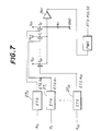
- An address transition detector is provided in, for example, the block of the address buffer 12a.
- FIG.7 is a block diagram of the address transition detector.
- the address transition detector is made up of conventional edge trigger circuits 270 - 2710 provided for the respective address bits A0 - A10, p-channel MOS transistors T0 - T10, an inverter INV, a resistor R1 and a pulse width controller PWC.
- the edge trigger circuits 200 - 2710 detect the edges of the corresponding address bits and generates edge trigger signals ETGA ⁇ 0- ETGA10 ⁇ , which are respectively applied to the gates of the transistors T0 - T10.
- the edge trigger signals ETGA0 ⁇ - ETGA10 ⁇ becomes active (low level)
- the corresponding transistor is turned ON, so that a high level is applied to the inverter INV.
- the inverter INV outputs a low level to the pulse width controller PWC, which generates the ATD pulse having a predetermined pulse duration.
- the internal voltage generator 39 is also configured in the same way as the circuit shown in FIG.4A.
- the internal voltage generator 39 generates an internal voltage V INT3 , which is regulated by the aforementioned sense amplifier driving clock ⁇ s generated by the clock generator 18.
- the internal voltage V INT3 is supplied to the sense system 400.
- the internal voltage V INT3 is equal to, for example, 4.0 volts.
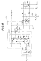
- FIG.8 is a circuit diagram of the internal voltage generator 39 and a part of the sense amplifier and I/O gate 24.
- the internal voltage generator 39 is made up of the aforementioned voltage regulator 100A, a one-shot pulse generator 60, the regulator transistor Q1, two n-channel MOS transistors Q40 and Q41.
- the gate of the regulator transistor Q1 is controlled by the voltage regulator 100A via the transistor Q40.
- the drain of the transistor Q41 is connected to the gate of the regulator transistor Q1, and the source of the transistor Q41 is grounded.
- the source of the regulator transistor Q1 is connected to a high-potential line 51.
- a sense amplifier SA is connected to a pair of bit lines BL and BL ⁇ , to which memory cells MC are connected, as shown in FIG.8.
- the memory cells MC shown in FIG.8 are respectively connected to word lines WL n and WL n+1 .
- the one-shot pulse generator 60 generates a one-shot pulse CLK1 ⁇ in synchronism with the sense amplifier driving signal ⁇ ⁇ s . More specifically, the one-shot pulse CLK1 ⁇ changes to the low level in synchronism with the fall of the sense amplifier driving signal ⁇ ⁇ s .
- the sense amplifier SA is also connected to the high-potential voltage line 51 and a low-potential voltage line 52.
- An n-channel MOS transistor Q42 is provided in the low-potential voltage line 52.
- the sense amplifier driving signals ⁇ s and ⁇ ⁇ s are maintained at the low and high levels, respectively.
- the transistor Q40 and Q41 are turned OFF and ON, respectively, so that the sense amplifier SA is substantially disconnected from the voltage lines 51 and 52.
- the clock signals ⁇ s and ⁇ ⁇ s are reversed, so that the sense amplifier SA starts to operate.
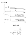
- the sense amplifier driving signal ⁇ ⁇ s changes from the high level to the low level, and as shown in FIG.9-(b), the one-shot pulse CLK1 ⁇ falls.
- the transistor Q30 is turned OFF, so that the gate voltage V G1 increases rapidly, as shown in FIG.9-(c). This rise of the gate voltage V G1 is slightly over-shooting.
- the one-shot pulse CLK1 ⁇ is not provided, the gate voltage V G1 will increase gradually from the ground potential, as illustrated by the broken line in FIG.9-(c).
- the internal voltage V INT3 increases rapidly in response to the rapid increase in the gate voltage V G1 .
- the internal voltage V INT3 will increases gradually if the one-shot pulse CLK1 ⁇ is not provided.
- the transistor Q30 is continuously or intermittently turned OFF, so that the gate voltage V G1 of the regulator transistor Q1 is increased.
- the RAS ⁇ signal is maintained in the high level (inactive state)
- the RAS ⁇ system 200 consumes a small amount of power, so that the transistor Q29 is short-circuited by the transistor Q30.
- the CAS ⁇ system 300 and the sense system 400 are also controlled in the same way as the RAS ⁇ system 200.
- the internal voltage V INT1 supplied to the RAS ⁇ system 200 is controlled separately from the internal voltage V INT2 supplied to the CAS ⁇ system 300.
- an n-channel MOS transistor Q31 is connected in parallel to the transistor Q30. The RAS ⁇ signal is applied to the gate of the transistor Q31, and the CAS ⁇ signal is applied to the gate of the transistor Q30.
- the gate voltage V G1 of the regulator transistor Q1 is increased.
- the refresh operation starts when the CAS signal changes to the low level before the RAS ⁇ signal changes to the low level. If the internal voltage compensation operation starts when the CAS ⁇ signal becomes the low level, the internal voltage will be compensated for excessively because the CAS system 300 does not operate in the CAS ⁇ -before- RAS ⁇ mode. In the configuration shown in FIG.10, when both the CAS ⁇ and RAS ⁇ signals are maintained in the low level, the compensation operation starts.
- the on-chip voltage regulator according to the present invention can be applied to not only DRAMs but also SRAMs.
- SRAMs a chip enable signal CE ⁇ and an output enable signal OE ⁇ are used as the clock signal CLK ⁇ .
- the present invention is suitable for logic LSIs.
Landscapes
- Engineering & Computer Science (AREA)
- Power Engineering (AREA)
- Microelectronics & Electronic Packaging (AREA)
- Automation & Control Theory (AREA)
- General Physics & Mathematics (AREA)
- Radar, Positioning & Navigation (AREA)
- Electromagnetism (AREA)
- Physics & Mathematics (AREA)
- Computer Hardware Design (AREA)
- Dram (AREA)
- Continuous-Control Power Sources That Use Transistors (AREA)
- Static Random-Access Memory (AREA)
- Semiconductor Integrated Circuits (AREA)
- Semiconductor Memories (AREA)
- Logic Circuits (AREA)
Claims (27)
- On-Chip-Spannungsregler zur Steuerung des Gates eines Regeltransistors (Q1), der einen ersten Anschluß besitzt, dem eine erste externe Versorgungsspannung (VEXT) zuführbar ist, und einen zweiten Anschluß, der mit einer internen Schaltung verbindbar ist, die auf einem Chip ausgebildet ist, auf dem der On-Chip-Spannungsregler ausgebildet ist,wobei der On-Chip-Spannungsregler aufweist:eine Taktempfangseineinrichtung (Q30) zum Empfang eines vorbestimmten Taktsignals

 und eine mit der Taktempfangseineinrichtung und dem Regeltransistor verbundene Regeleinrichtung (I, Q26 - Q30, Q31) zur Erzeugung einer an das Gate des Regeltransistors ausgegebenen Gatespannung (VG1) auf der Basis eines Zustands des vorbestimmten Taktsignals derart, daß der Regeltransistor unabhängig davon, ob die interne Schaltung in Betrieb ist oder nicht, aus der externen Spannung eine im wesentlichen feste interne Spannung (VINT) erzeugen kann,dadurch gekennzeichnet,daß dem Gate des Regeltransistors (Q1) eine Kapazität (C) hinzugefügt ist,und daß das Gate-Potential des Regeltransistors (Q1) auf der Basis der aktiven Periode des Taktsignals oder seiner Frequenz gesteuert wird.
 - On-Chip-Spannungsregler nach Anspruch 1,dadurch gekennzeichnet,daß die Regeleinrichtung Mittel (I, Q26 - Q30) aufweist zur Ausgabe einer ersten Gatespannung (V₁), die dem Gate des Regeltransistors zugeführt wird, wenn das vorbestimmte Taktsignal in einem ersten Zustand gehalten wird, und zur Erzeugung einen zweiten Gatespannung (V1 + V2), die dem Gate des Regeltransistors zugeführt wird, wenn das vorbestimmte Taktsignal in einem zweiten Zustand gehalten wird.
- On-Chip-Spannungsregler nach Anspruch 1,dadurch gekennzeichnet,daß der Spannungsregler Mittel (I, Q26 - Q30) aufweist zur Erhöhung der an das Gate des Regeltransistors ausgegebenen Gatespannung, wenn das vorbestimmte Taktsignal von einem ersten Zustand, der anzeigt, ob die interne Schaltung in einem Bereitschaftsmodus gehalten wird, in einen zweiten Zustand wechselt, der anzeigt, daß die interne Schaltung in Betrieb ist.
- On-Chip-Spannungsregler nach Anspruch 1,dadurch gekennzeichnet,daß der On-Chip-Spannungsregler ferner eine Impulsgeneratoreinrichtung (60) aufweist zur Erzeugung des genannten vorbestimmten Taktsignals aus einem Zustandskennzeichnungssignal, das anzeigt, ob die interne Schaltung in Betrieb ist oder nicht.
- On-Chip-Spannungsregler nach Anspruch 4,dadurch gekennzeichnet,daß die Impulsgeneratoreinrichtung einen Einzelimpuls (

- On-Chip-Spannungsregler nach Anspruch 1,dadurch gekennzeichnet,daß der On-Chip-Spannungsregler eine Impulsgeneratoreinrichtung (Q30, Q31) zum Empfang einer Mehrzahl von Zustandskennzeichnungssignalen (


- On-Chip-Spannungsregler nach Anspruch 1,dadurch gekennzeichnet,daß Regeleinrichtung aufweist:eine Konstantstromquelle (I), der eine erste vorbestimmte Versorgungsspannung (VA, VEXT) zuführbar ist,eine zu der Konstantstromquelle in Reihe geschaltete und mit dem Gate des Regeltransistors verbundene erste Spannungsgeneratoreinrichtung (Q26 - Q28) zur Erzeugung einer ersten Spannung (V1) aus einem von der Konstantstromquelle erzeugte Konstantstrom,eine zu der ersten Spannungsgeneratoreinrichtung in Reihe geschaltete zweite Spannungsgeneratoreinrichtung (Q29), der eine vorbestimmte Versorgungsspannung (Massepegel) zuführbar ist, die niedriger ist als die erste vorbestimmte Spannung, zur Erzeugung einer zweiten Spannung (V2) aus dem Konstantstrom, der von der Konstantstromquelle über die erste Spannungsgeneratoreinrichtung zugeführt wird, undeine mit der zweiten Spannungsgeneratoreinrichtung verbundene Steuereinrichtung (Q29) zum selektiven Kurzschließen der zweiten Spannungsgeneratoreinrichtung auf der Basis des Zustands des vorbestimmten Taktsignals, so daß wahlweise entweder die Summe (V1 + V2) aus der ersten und der zweiten Spannung oder die erste Spannung als die genannte Gatespannung an das Gate des Regeltransistors ausgegeben wird.
- On-Chip-Spannungsregler nach Anspruch 7,dadurch gekennzeichnet,daß die erste Spannungsgeneratoreinrichtung m Feldeffekttransistoren (Q26 - Q28) aufweist, wobei m ganzzahlig und gleich oder größer als 1 ist,daß die m Feldeffekttransistoren als Dioden geschaltet und in Reihenschaltung angeordnet sind, unddaß die erste Spannung im wesentlichen der Summe der Schwellwertspannungen der m Feldeffekttransistoren entspricht.
- On-Chip-Spannungsregler nach Anspruch 7,dadurch gekennzeichnet,daß die zweite Spannungsgeneratoreinrichtung n Feldeffekttransistoren (Q9) aufweist, wobei n ganzzahlig und gleich oder größer als 1 ist,daß die n Feldeffekttransistoren als Dioden geschaltet und in Reihenschaltung angeordnet sind, unddaß die zweite Spannung im wesentlichen der Summe der Schwellwertspannungen der n Feldeffekttransistoren entspricht.
- On-Chip-Spannungsregler nach Anspruch 7,dadurch gekennzeichnet,daß die Steuereinrichtung einen Transistor (Q30) enthält mit einem Steueranschluß, dem das vorbestimmte Taktsignal (


- On-Chip-Spannungsregler nach Anspruch 7,dadurch gekennzeichnet,daß die Konstantstromquelle einen Feldeffekttransistor (Q25) vom Verarmungstyp aufweist unddaß der Feldeffekttransistor der Konstantstromquelle einen Gateanschluß besitzt, ferner einen ersten Anschluß, dem die erste vorbestimmte Versorgungsspannung zuführbar ist, sowie einen zweiten Anschluß, der mit dem Gateanschluß und dem Gate des Regeltransistors verbunden ist.
- On-Chip-Spannungsregler nach Anspruch 11,dadurch gekennzeichnet,daß der Feldeffekttransistor aufweist:ein Substrat (1) eines ersten Leitfähigkeitstyps,einen in dem Substrat ausgebildeten ersten Graben (2) von einem dem ersten Leitfähigkeitstyp entgegengesetzten zweiten Leitfähigkeitstyp,einen in dem ersten Graben ausgebildeten zweiten Graben (3) des ersten Leitfähigkeitstyps,eine in dem zweiten Graben ausgebildete erste Diffusionsregion (S) des zweiten Leitfähigkeitstyps, die dem ersten Anschluß entspricht,eine in dem zweiten Graben ausgebildete zweite Diffusionsregion (D) des zweiten Leitfähigkeitstyps, die dem zweiten Anschluß entspricht,und ein zwischen der ersten und der zweiten Diffusionsregion angeordnetes Gate (G), das dem Gateanschluß entspricht.
- On-Chip-Spannungsregler nach Anspruch 12,dadurch gekennzeichnet,daß dem ersten Graben die externe Versorgungsspannung (VEXT) zuführbar ist.
- On-Chip-Spannungsregler nach Anspruch 11,dadurch gekennzeichnet,daß die erste vorbestimmte Versorgungsspannung gleich der externen Versorgungsspannung ist.
- On-Chip-Spannungsregler nach Anspruch 11,dadurch gekennzeichnet,daß der Feldeffekttransistor aufweist:ein Substrat (4) eines ersten Leitfähigkeitstyps,einen in dem Substrat ausgebildeten Graben (5) von einem dem ersten Leitfähigkeitstyp entgegengesetzten zweiten Leitfähigkeitstyp,eine in dem Graben ausgebildete erste Diffusionsregion (S) des ersten Leitfähigkeitstyps, die dem ersten Anschluß entspricht,eine in dem Graben ausgebildete zweite Diffusionsregion (D) des ersten Leitfähigkeitstyps, die dem zweiten Anschluß entspricht,und ein zwischen der ersten und der zweiten Diffusionsregion angeordnetes Gate (G), das dem Gateanschluß entspricht.
- On-Chip-Spannungsregler nach Anspruch 15,dadurch gekennzeichnet,daß dem ersten Graben die externe Versorgungsspannung zuführbar ist.
- On-Chip-Spannungsregler nach Anspruch 7,dadurch gekennzeichnet,daß der On-Chip-Spannungsregler einen Kondensator aufweist mit einem ersten Anschluß, der mit dem Gate des Regeltransistors verbunden ist, und einem zweiten Anschluß, dem die genannte Referenzspannung zuführbar ist.
- On-Chip-Spannungsregler nach Anspruch 1,dadurch gekennzeichnet,daß die Regeleinrichtung Mittel (Q26 - Q30) aufweist zur Änderung des inneren Widerstands des Regeltransistors auf der Basis des Zustands des vorbestimmten Taktes.
- On-Chip-Spannungsregler nach Anspruch 1,dadurch gekennzeichnet,daß die Regeleinrichtung aufweist:eine Konstantstromgeneratoreinrichtung (I) zur Erzeugung eines Konstantstroms undmit der Konstantstromgeneratoreinrichtung und dem Regeltransistor verbundene variable Widerstandselemente (Q29 - Q30) zur Bereitstellung eines variablen Widerstands in Abhängigkeit vom Zustand des vorbestimmten Taktes und zur Ausgabe einer Spannung (V1, V1 + V2), die durch den Durchgang des Konstantstroms durch die variablen Widerstandselemente zu dem Gate des Regeltransistors gewonnen wird.
- On-Chip-Spannungsregler nach Anspruch 1,dadurch gekennzeichnet,daß der Regler in einer internen Schaltung enthalten ist und daß diese interne Schaltung eine Halbleiterspeicheranordnung ist miteinem ersten System (300), das nach Maßgabe eines ersten Taktsignals (φs,
 einem zweiten System (200), das nach Maßgabe eines zweiten Taktsignals (
 einem dritten System, das nach Maßgabe eines dritten Taktsignals (ATD,
 wobei die Einrichtung (500) zur internen Spannungserzeugung mit dem ersten, zweiten und dritten System verbunden ist, um aus der externen Versorgungsspannung (VEXT) auf der Basis des ersten, zweiten und dritten Taktsignals eine erste, zweite bzw. dritte interne Spannungen (VINT1, VINT2, VINT3) zu erzeugen und diese erste, zweite bzw. dritte interne Spannung an das erste, zweite bzw. dritte System auszugeben,und daß die Einrichtung zur internen Spannungserzeugung ausgestattet ist mitjeweils einem Regeltransistor (Q1) für das erste, zweite und dritte System mit einem ersten Anschluß, dem die externe Spannung zuführbar ist, und einem zweiten Anschluß, der mit einem korrespondierenden Anschluß des ersten, zweiten bzw. dritten Systems verbunden ist, undeiner mit jedem der Regeltransistoren verbundenen Regeleinrichtung zur Erzeugung einer an das Gate des Regeltransistors ausgegebenen Gatespannung (VG1) auf der Basis des Zustands wenigstens eines aus dem ersten, zweiten und dritten Taktsignal, so daß von der ersten, zweiten und dritten Spannung unabhängig davon, ob von dem ersten, zweiten und dritten System eines in Betrieb ist, die entsprechende Spannung im wesentlichen fest ist.
 - On-Chip-Spannungsregler nach Anspruch 20,dadurch gekennzeichnet,daß die Regeleinrichtung Mittel (39) aufweist zum Steuern der an das Gate des für das erste System vorgesehenen Regeltransistors ausgegebenen Gatespannung auf der Basis des Zustands des ersten Taktsignals undund daß das erste Taktsignal mit einem Leseverstärkertreibersignal (φs,

- On-Chip-Spannungsregler nach Anspruch 21, gekennzeichnet durch eine Impulsgeneratoreinrichtung zur Erzeugung eines Einzelimpulses (

- On-Chip-Spannungsregler nach Anspruch 20,dadurch gekennzeichnet,daß die Regeleinrichtung Mittel (38) aufweist zur Erzeugung der an das Gate des für das zweite System vorgesehenen Regeltransistors ausgegebenen Gatespannung auf der Basis des Zustands des zweiten Taktsignals,und daß das zweite Taktsignal ein Zeilenaddressen-Tastsignal ist, das von einer externen Vorrichtung zugeführt wird.
- On-Chip-Spannungsregler nach Anspruch 20,dadurch gekennzeichnet,daß die Regeleinrichtung Mittel (39) aufweist zum Steuern der an das Gate des für das zweite System vorgesehenen Regeltransistors ausgegebenen Gatespannung auf der Basis des Zustands des zweiten Taktsignals,und daß die Halbleiterspeicheranordnung eine Adressen-Ubergangsdetektoreinrichtung (27₀, - 27₁₀, T₀ - T₁₀, R1, INV, PWC) aufweist zum Detektieren einer Änderung in der externen Adresse und zur Ausgabe eines Impulssignals (ATD), wenn die Änderung in der externen Adresse detektiert wird, wobei das Impulssignal dem zweiten Taktsignal entspricht.
- On-Chip-Spannungsregler nach Anspruch 20,dadurch gekennzeichnet,daß die Regeleinrichtung Mittel (Q26 - Q31) aufweist zur Erzeugung der an das Gate des jeweils für das zweite und dritte System vorgesehenen Regeltransistors ausgegebenen Gatespannung auf der Basis der Zustände des zweiten und dritten Taktsignals (


- On-Chip-Spannungsregler (Q1) nach Anspruch 1,dadurch gekennzeichnet,daß der Regler eine integrierte Halbleiterschaltungsanordnung istund daß diese integrierte Halbleiterschaltungsanordnung mit dem On-Chip-Spannungsregler verbundene Mittel (100, 100A) aufweist zur Steuerung des Stromführungsvermögens des On-Chip-Spannungsreglers derart, daß das Stromführungsvermögen, das erhalten wird, wenn die interne Schaltung in einem aktiven Zustand gehalten wird, größer ist als das Stromführungsvermögen, das erhalten wird, wenn die interne Schaltung in einem inaktivem Zustand gehalten wird.
- On-Chip-Spannungsregler nach Anspruch 26,dadurch gekennzeichnet,daß mit dem Gate des Regeltransistors des On-Chip-Spannungsreglers Mittel (100, 100A) verbunden sind zur Änderung des inneren Widerstands des Regeltransistors entsprechend dem Takt, der die aktiven/inaktiven Zustände der internen Schaltung der integrierten Halbleiterschaltungsanordnung steuert, um dadurch eine Differenz zu unterdrücken zwischen der internen Versorgungsspannung, die erreicht wird, wenn die interne Schaltung im aktiven Zustand gehalten wird, und der internen Versorgungsspannung, die erreicht wird, wenn die interne Schaltung im inaktiven Zustand gehalten wird.
Applications Claiming Priority (2)
| Application Number | Priority Date | Filing Date | Title |
|---|---|---|---|
| JP83760/90 | 1990-03-30 | ||
| JP8376090 | 1990-03-30 |
Publications (3)
| Publication Number | Publication Date |
|---|---|
| EP0449310A2 EP0449310A2 (de) | 1991-10-02 |
| EP0449310A3 EP0449310A3 (en) | 1992-02-05 |
| EP0449310B1 true EP0449310B1 (de) | 1996-03-13 |
Family
ID=13811526
Family Applications (1)
| Application Number | Title | Priority Date | Filing Date |
|---|---|---|---|
| EP91105071A Expired - Lifetime EP0449310B1 (de) | 1990-03-30 | 1991-03-28 | On-Chip-Spannungsregler und Halbleiterspeichervorrichtung mit Verwendung desgleichen |
Country Status (5)
| Country | Link |
|---|---|
| US (1) | US5097303A (de) |
| EP (1) | EP0449310B1 (de) |
| JP (1) | JP3124781B2 (de) |
| KR (1) | KR940009835B1 (de) |
| DE (1) | DE69117784T2 (de) |
Families Citing this family (34)
| Publication number | Priority date | Publication date | Assignee | Title |
|---|---|---|---|---|
| JP3068291B2 (ja) * | 1990-12-12 | 2000-07-24 | 新日本製鐵株式会社 | 半導体記憶装置 |
| JPH04333277A (ja) * | 1991-05-09 | 1992-11-20 | Nec Ic Microcomput Syst Ltd | 半導体メモリ装置 |
| US5253205A (en) * | 1991-09-05 | 1993-10-12 | Nippon Steel Semiconductor Corporation | Bit line and cell plate clamp circuit for a DRAM |
| JPH06236686A (ja) * | 1993-01-22 | 1994-08-23 | Nec Corp | 半導体装置 |
| US5515319A (en) * | 1993-10-12 | 1996-05-07 | Texas Instruments Incorporated | Non-volatile memory cell and level shifter |
| EP0661717B1 (de) * | 1993-12-31 | 2000-03-29 | STMicroelectronics S.r.l. | Spannungsregler zum Programmieren nichtflüchtiger und elektrisch programmierbarer Speicherzellen |
| US5786720A (en) * | 1994-09-22 | 1998-07-28 | Lsi Logic Corporation | 5 volt CMOS driver circuit for driving 3.3 volt line |
| US5721485A (en) * | 1996-01-04 | 1998-02-24 | Ibm Corporation | High performance on-chip voltage regulator designs |
| US5663919A (en) * | 1996-02-28 | 1997-09-02 | Micron Technology, Inc. | Memory device with regulated power supply control |
| US5999039A (en) * | 1996-09-30 | 1999-12-07 | Advanced Micro Devices, Inc. | Active power supply filter |
| JP3963990B2 (ja) * | 1997-01-07 | 2007-08-22 | 株式会社ルネサステクノロジ | 内部電源電圧発生回路 |
| US5818291A (en) * | 1997-04-04 | 1998-10-06 | United Memories, Inc. | Fast voltage regulation without overshoot |
| US7467379B2 (en) * | 2001-01-16 | 2008-12-16 | International Business Machines Corporation | System and method for incrementally executing a client/server application |
| US20030122173A1 (en) * | 2001-12-28 | 2003-07-03 | Rabadam Eleanor P. | Package for a non-volatile memory device including integrated passive devices and method for making the same |
| US6498737B1 (en) * | 2002-01-16 | 2002-12-24 | Taiwan Semiconductor Manufacturing Company | Voltage regulator with low sensitivity to body effect |
| US6850856B1 (en) * | 2002-11-18 | 2005-02-01 | Sun Microsystems, Inc. | I/O receiver thermal correction scheme |
| US6924692B2 (en) * | 2003-06-30 | 2005-08-02 | Intel Corporation | Voltage reference generator |
| US7554312B2 (en) * | 2003-06-30 | 2009-06-30 | Intel Corporation | DC-to-DC voltage converter |
| US7170308B1 (en) * | 2003-07-28 | 2007-01-30 | Altera Corporation | On-chip voltage regulator using feedback on process/product parameters |
| US7119604B2 (en) * | 2004-06-17 | 2006-10-10 | Taiwan Semiconductor Manufacturing Company, Ltd. | Back-bias voltage regulator having temperature and process variation compensation and related method of regulating a back-bias voltage |
| US7151697B2 (en) * | 2004-11-30 | 2006-12-19 | Infineon Technologies Ag | Non-volatile semiconductor memory |
| JP4761833B2 (ja) * | 2005-05-24 | 2011-08-31 | 株式会社東芝 | 半導体装置及びシステム |
| US8624636B2 (en) | 2006-05-22 | 2014-01-07 | Brillouin Energy Corp. | Drive circuit and method for semiconductor devices |
| US20070268045A1 (en) * | 2006-05-22 | 2007-11-22 | Profusion Energy, Inc. | Drive Circuit And Method For Semiconductor Devices |
| JP4960179B2 (ja) * | 2007-08-28 | 2012-06-27 | ルネサスエレクトロニクス株式会社 | データ処理装置、電源電圧生成回路及びその電源電圧生成方法 |
| US7919840B2 (en) * | 2007-11-20 | 2011-04-05 | International Business Machines Corporation | Integrated non-isolated VRM and microprocessor assembly |
| US7705685B2 (en) * | 2007-12-06 | 2010-04-27 | Hong Kong Applied Science And Technology Research Institute Co., Ltd. | Low-voltage oscillator with capacitor-ratio selectable duty cycle |
| JP2009164415A (ja) * | 2008-01-08 | 2009-07-23 | Mitsumi Electric Co Ltd | 半導体装置 |
| JP2010157277A (ja) * | 2008-12-26 | 2010-07-15 | Toshiba Corp | 不揮発性半導体記憶装置 |
| JP5593904B2 (ja) * | 2010-07-16 | 2014-09-24 | 株式会社リコー | 電圧クランプ回路およびこれを用いた集積回路 |
| EP3295310A4 (de) | 2015-05-14 | 2018-12-26 | Adesto Technologies Corporation | Gleichzeitige lese- und rekonfigurierte schreiboperationen in einer speichervorrichtung |
| JP1643024S (de) * | 2019-03-15 | 2019-10-07 | ||
| US12136921B2 (en) * | 2020-02-19 | 2024-11-05 | Rohm Co., Ltd. | Clamp circuit |
| US11955196B2 (en) * | 2022-07-13 | 2024-04-09 | Nanya Technology Corporation | Memory device, voltage generating device and voltage generating method thereof |
Family Cites Families (12)
| Publication number | Priority date | Publication date | Assignee | Title |
|---|---|---|---|---|
| JPS5780828A (en) * | 1980-11-07 | 1982-05-20 | Hitachi Ltd | Semiconductor integrated circuit device |
| JPS58105563A (ja) * | 1981-12-17 | 1983-06-23 | Mitsubishi Electric Corp | 基板バイアス発生回路 |
| US4491938A (en) * | 1981-12-28 | 1985-01-01 | Texas Instruments Incorporated | Low voltage RAM cell |
| JPS59218042A (ja) * | 1983-05-26 | 1984-12-08 | Toshiba Corp | 半導体集積回路 |
| JPS60176121A (ja) * | 1984-02-22 | 1985-09-10 | Toshiba Corp | 電圧降下回路 |
| JPS60179998A (ja) * | 1984-02-28 | 1985-09-13 | Fujitsu Ltd | 電圧検出回路 |
| JPS6199363A (ja) * | 1984-10-19 | 1986-05-17 | Mitsubishi Electric Corp | 基板電位発生回路 |
| US4698789A (en) * | 1984-11-30 | 1987-10-06 | Kabushiki Kaisha Toshiba | MOS semiconductor device |
| JPS61163655A (ja) * | 1985-01-14 | 1986-07-24 | Toshiba Corp | 相補型半導体集積回路 |
| JPS6273489A (ja) * | 1985-09-25 | 1987-04-04 | Mitsubishi Electric Corp | 不揮発性半導体記憶装置 |
| US4973922A (en) * | 1987-11-27 | 1990-11-27 | At&T Bell Laboratories | Voltage controlled variable capacitor and oscillator using it |
| US5046052A (en) * | 1988-06-01 | 1991-09-03 | Sony Corporation | Internal low voltage transformation circuit of static random access memory |
-
1991
- 1991-03-19 JP JP03055150A patent/JP3124781B2/ja not_active Expired - Lifetime
- 1991-03-28 EP EP91105071A patent/EP0449310B1/de not_active Expired - Lifetime
- 1991-03-28 DE DE69117784T patent/DE69117784T2/de not_active Expired - Fee Related
- 1991-03-29 US US07/677,560 patent/US5097303A/en not_active Expired - Lifetime
- 1991-03-30 KR KR1019910005205A patent/KR940009835B1/ko not_active Expired - Fee Related
Also Published As
| Publication number | Publication date |
|---|---|
| DE69117784D1 (de) | 1996-04-18 |
| US5097303A (en) | 1992-03-17 |
| EP0449310A3 (en) | 1992-02-05 |
| KR910017630A (ko) | 1991-11-05 |
| JPH04212782A (ja) | 1992-08-04 |
| JP3124781B2 (ja) | 2001-01-15 |
| DE69117784T2 (de) | 1996-10-24 |
| EP0449310A2 (de) | 1991-10-02 |
| KR940009835B1 (ko) | 1994-10-17 |
Similar Documents
| Publication | Publication Date | Title |
|---|---|---|
| EP0449310B1 (de) | On-Chip-Spannungsregler und Halbleiterspeichervorrichtung mit Verwendung desgleichen | |
| US6492863B2 (en) | Internal high voltage generation circuit capable of stably generating internal high voltage and circuit element therefor | |
| JP3510335B2 (ja) | 半導体記憶装置、内部電源電圧発生回路、内部高電圧発生回路、中間電圧発生回路、定電流源、および基準電圧発生回路 | |
| KR940001640B1 (ko) | 반도체 집적 회로장치 | |
| US5442277A (en) | Internal power supply circuit for generating internal power supply potential by lowering external power supply potential | |
| US6535435B2 (en) | Reference voltage generator permitting stable operation | |
| US6954103B2 (en) | Semiconductor device having internal voltage generated stably | |
| US6351178B1 (en) | Reference potential generating circuit | |
| JP4353621B2 (ja) | 半導体装置 | |
| KR20030037266A (ko) | 내부 전압 레벨 제어 회로 및 반도체 기억 장치 및 그들의제어 방법 | |
| JP2003068079A (ja) | 半導体記憶回路 | |
| JPH09231751A (ja) | 半導体記憶装置 | |
| US20010050878A1 (en) | Semiconductor memory device and control method | |
| US6121812A (en) | Delay circuit having delay time free from influence of operation environment | |
| KR100331549B1 (ko) | 더미 비트 라인을 이용한 전류 센스 앰프 회로 | |
| CN111833923A (zh) | 用于排放泄漏电流的系统和装置 | |
| US5774405A (en) | Dynamic random access memory having an internal circuit using a boosted potential | |
| US6330173B1 (en) | Semiconductor integrated circuit comprising step-up voltage generation circuit | |
| KR19990029191A (ko) | 저전압 동작 특성이 개선된 반도체 집적 회로 장치 | |
| US6614270B2 (en) | Potential detecting circuit having wide operating margin and semiconductor device including the same | |
| US5875145A (en) | Semiconductor memory device having a voltage lowering circuit of which supplying capability increases when column system is in operation | |
| US4875195A (en) | Semiconductor device with a reference voltage generator | |
| US5990729A (en) | Semiconductor integrated circuit having first and second voltage step down circuits | |
| US9001610B2 (en) | Semiconductor device generating internal voltage | |
| KR100256129B1 (ko) | 기판 바이어스전위 발생장치 |
Legal Events
| Date | Code | Title | Description |
|---|---|---|---|
| PUAI | Public reference made under article 153(3) epc to a published international application that has entered the european phase |
Free format text: ORIGINAL CODE: 0009012 |
|
| AK | Designated contracting states |
Kind code of ref document: A2 Designated state(s): DE FR GB IT |
|
| PUAL | Search report despatched |
Free format text: ORIGINAL CODE: 0009013 |
|
| AK | Designated contracting states |
Kind code of ref document: A3 Designated state(s): DE FR GB IT |
|
| 17P | Request for examination filed |
Effective date: 19920728 |
|
| 17Q | First examination report despatched |
Effective date: 19940511 |
|
| GRAH | Despatch of communication of intention to grant a patent |
Free format text: ORIGINAL CODE: EPIDOS IGRA |
|
| GRAA | (expected) grant |
Free format text: ORIGINAL CODE: 0009210 |
|
| AK | Designated contracting states |
Kind code of ref document: B1 Designated state(s): DE FR GB IT |
|
| PG25 | Lapsed in a contracting state [announced via postgrant information from national office to epo] |
Ref country code: FR Effective date: 19960313 |
|
| REF | Corresponds to: |
Ref document number: 69117784 Country of ref document: DE Date of ref document: 19960418 |
|
| ITF | It: translation for a ep patent filed | ||
| EN | Fr: translation not filed | ||
| PLBE | No opposition filed within time limit |
Free format text: ORIGINAL CODE: 0009261 |
|
| STAA | Information on the status of an ep patent application or granted ep patent |
Free format text: STATUS: NO OPPOSITION FILED WITHIN TIME LIMIT |
|
| 26N | No opposition filed | ||
| REG | Reference to a national code |
Ref country code: GB Ref legal event code: IF02 |
|
| REG | Reference to a national code |
Ref country code: GB Ref legal event code: 732E |
|
| PGFP | Annual fee paid to national office [announced via postgrant information from national office to epo] |
Ref country code: GB Payment date: 20090325 Year of fee payment: 19 |
|
| PGFP | Annual fee paid to national office [announced via postgrant information from national office to epo] |
Ref country code: DE Payment date: 20090327 Year of fee payment: 19 Ref country code: IT Payment date: 20090321 Year of fee payment: 19 |
|
| GBPC | Gb: european patent ceased through non-payment of renewal fee |
Effective date: 20100328 |
|
| PG25 | Lapsed in a contracting state [announced via postgrant information from national office to epo] |
Ref country code: DE Free format text: LAPSE BECAUSE OF NON-PAYMENT OF DUE FEES Effective date: 20101001 |
|
| PG25 | Lapsed in a contracting state [announced via postgrant information from national office to epo] |
Ref country code: IT Free format text: LAPSE BECAUSE OF NON-PAYMENT OF DUE FEES Effective date: 20100328 Ref country code: GB Free format text: LAPSE BECAUSE OF NON-PAYMENT OF DUE FEES Effective date: 20100328 |