EP0449319B1 - Schaltung zur Mikrofoniereduzierung - Google Patents
Schaltung zur Mikrofoniereduzierung Download PDFInfo
- Publication number
- EP0449319B1 EP0449319B1 EP91105092A EP91105092A EP0449319B1 EP 0449319 B1 EP0449319 B1 EP 0449319B1 EP 91105092 A EP91105092 A EP 91105092A EP 91105092 A EP91105092 A EP 91105092A EP 0449319 B1 EP0449319 B1 EP 0449319B1
- Authority
- EP
- European Patent Office
- Prior art keywords
- circuit
- capacitor
- voltage
- microphony
- capacitors
- Prior art date
- Legal status (The legal status is an assumption and is not a legal conclusion. Google has not performed a legal analysis and makes no representation as to the accuracy of the status listed.)
- Expired - Lifetime
Links
- 239000003990 capacitor Substances 0.000 claims abstract description 43
- 239000000919 ceramic Substances 0.000 claims abstract description 9
- 102220511583 Kappa-casein_N10A_mutation Human genes 0.000 claims description 3
- 238000000034 method Methods 0.000 abstract description 4
- 239000003985 ceramic capacitor Substances 0.000 description 6
- 229910052715 tantalum Inorganic materials 0.000 description 5
- GUVRBAGPIYLISA-UHFFFAOYSA-N tantalum atom Chemical compound [Ta] GUVRBAGPIYLISA-UHFFFAOYSA-N 0.000 description 5
- 230000008859 change Effects 0.000 description 4
- 230000000694 effects Effects 0.000 description 3
- 238000002474 experimental method Methods 0.000 description 3
- 230000004044 response Effects 0.000 description 3
- 230000009471 action Effects 0.000 description 2
- 238000013461 design Methods 0.000 description 2
- 238000010586 diagram Methods 0.000 description 2
- 230000008030 elimination Effects 0.000 description 2
- 238000003379 elimination reaction Methods 0.000 description 2
- 238000004519 manufacturing process Methods 0.000 description 2
- 230000003321 amplification Effects 0.000 description 1
- 238000013459 approach Methods 0.000 description 1
- 230000005540 biological transmission Effects 0.000 description 1
- 238000010276 construction Methods 0.000 description 1
- 230000008878 coupling Effects 0.000 description 1
- 238000010168 coupling process Methods 0.000 description 1
- 238000005859 coupling reaction Methods 0.000 description 1
- 230000001627 detrimental effect Effects 0.000 description 1
- 230000006870 function Effects 0.000 description 1
- 238000009863 impact test Methods 0.000 description 1
- 238000009434 installation Methods 0.000 description 1
- 238000003199 nucleic acid amplification method Methods 0.000 description 1
- 230000010355 oscillation Effects 0.000 description 1
- 230000009467 reduction Effects 0.000 description 1
- 239000000758 substrate Substances 0.000 description 1
- 238000012360 testing method Methods 0.000 description 1
Images



Classifications
-
- H—ELECTRICITY
- H03—ELECTRONIC CIRCUITRY
- H03L—AUTOMATIC CONTROL, STARTING, SYNCHRONISATION OR STABILISATION OF GENERATORS OF ELECTRONIC OSCILLATIONS OR PULSES
- H03L7/00—Automatic control of frequency or phase; Synchronisation
- H03L7/06—Automatic control of frequency or phase; Synchronisation using a reference signal applied to a frequency- or phase-locked loop
- H03L7/08—Details of the phase-locked loop
- H03L7/085—Details of the phase-locked loop concerning mainly the frequency- or phase-detection arrangement including the filtering or amplification of its output signal
- H03L7/093—Details of the phase-locked loop concerning mainly the frequency- or phase-detection arrangement including the filtering or amplification of its output signal using special filtering or amplification characteristics in the loop
Definitions
- the invention relates to a circuit for reducing microphony which includes ceramic surface-mounted capacitors.
- Microphony of a ceramic capacitor means that the voltage between the capacitor terminals changes under mechanical action.
- the mechanical action may consist of impacts or vibration, causing deformation of the capacitor and appearing, for example, in a radio telephone which is portable or installed in an automobile.
- Efforts have been made to reduce microphony by placing the critical capacitors in a location where their fastening is as firm as possible, i.e. where their deformation is minimal. Special attention must also be paid to the fastening of the printed circuit board which serves as the substrate for the surface-mounted capacitor.
- a mechanical radio receiver tuner with microphonics elimination circuitry is for example known from WO 82/01292.
- the mechanical position of a movable tuning element provides an associated adjustable reactance which determines a control voltage for controlling the output of a voltage controlled oscillator that serves as the local oscillator for a superheterodyne radio receiver.
- a switch disconnects the movable tuning element from operative control of the local oscillator frequency and implement as a locked tuning mode by providing the voltage controlled oscillator with a control voltage related to the difference between the frequency of the output signal of a mixer stage and the center frequency of a fixed tuned narrow passband IF stage that follows the mixer.
- the switching circuit reimplements the tuning mode so that the position of the mechanically movable element will once again control the output of the local oscillator. In this manner, minor changes in the mechanical position of the movable tuning element during the locked tuning mode have no effect on receiver tuning and therefore microphonics are substantially eliminated.
- the object of the invention is thus to find for the problem a new solution by which the effects of the microphony of ceramic surface-mounted capacitors are reduced.
- a circuit is presented in Claim 1 as a solution to this problem. If the direct voltage effective across the capacitor is eliminated, microphony does not substantially cause non-desirable interference voltage.
- Embodiments of the invention are presented in the non-independent claims.
- the loop filter is a filter coupled between the phase comparator and the VCO, here a second-degree active filter by means of which the operating parameters of the loop are determined at the frequency and time levels (e.g. settling time, modulation response).
- the loop filter functions within the audio frequency range, the typical cut-off frequency of the low-pass stage being approx. 200 Hertz. With practical component values, this usually leads to the use of components in an order of magnitude of 10 - 47 nF. Implemented by the surface-mounting technique, ceramic components of this magnitude are quite microphonic. Passive-stage capacitors connected after the active loop filter are particularly prone to develop microphony, since even an interference voltage of 1 millivolt in the VCO control line corresponds the highest possible speech volume as the modulation of the transmission signal of a mobile telephone.
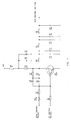
- Figure 1 depicts the circuit diagram of the loop filter of the frequency synthesizer used in a radio telephone. This circuit has been implemented using surface-mounted components. In the loop filter the ceramic surface-mounted capacitors C30 - C33 (22 nF) to the right of the transistor pair V20 are coupled between the signal lead and the ground. When the circuit board is subjected to an impact, owing to the microphony of the capacitors an interference voltage with a strongly varying amplitude is produced in the circuit (in the output VCO Control Voltage).
- the invention is based on an idea model of the production of a non-desirable, i.e. interference voltage: when a capacitor is bent mechanically, its capacitance value changes. Since the electric charge of the capacitor remains unchanged (electrons do not disappear), from this follows between the capacitor terminals a voltage change proportional to the change in the component value, i.e. the capacitance.
- interference voltage (change in capacitance) x (voltage effective across the capacitor)
- Figure 2 depicts an oscillogram which shows the strong impact response (oscillation of the voltage) of the capacitor.
- Channel 2 (indicated by CH2 gnd) has the interference voltage caused by the capacitor coupled according to the principle of Figure 1
- channel 1 indicated by CH1 gnd
- the ceramic piece capacitor e.g. C30
- the oscilloscope settings and test coupling amplifications were fully identical.
- the effect of the invention was verified, i.e. the reduction of the interference voltage, even to the extent that the arrangement according to the invention can be deemed to prevent substantially the production of an interference voltage due to capacitor microphony.
- a method for reducing microphony can be implemented by arranging a circuit according to the invention which eliminates the direct voltage effective across ceramic capacitors.
- the loop filter circuit of Figure 1 is used as an example.
- the signal ground of the capacitors was separated from the actual ground potential by means of a tantalum capacitor.
- Figure 3 depicts a circuit like this, with a tantalum capacitor C40 (1 ⁇ F).
- microphony may appear on the ceramic capacitors C30 - C36 (22 nF).
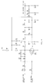
- Figure 5 finally depicts a loop filter implemented using operational amplifiers.
- the operational amplifiers N10A and N10B are coupled in such a manner that they actively cancel any possible direct-voltage differential V1-V2.
- the apparent ground potential is formed by a tantalum capacitor C40 (10 ⁇ F).
- FIG. 3 A comparison of Figures 3 - 5 to the loop filter according to Figure 1 shows that they have certain additional components due to practical circuit design.
- the components essential from the viewpoint of the invention were mentioned above in connection with the figures. It is hardly necessary to describe the operation of the circuits of Figures 1, 3 - 5 in greater detail in this context, since it is evident for an expert in the art and does not as such relate to the application of the invention.
- the described loop filter of a frequency synthesizer is only one example of the circuits which according to the invention can be applied for reducing microphony.
Landscapes
- Filters And Equalizers (AREA)
- Networks Using Active Elements (AREA)
- Reverberation, Karaoke And Other Acoustics (AREA)
- Measurement Of Velocity Or Position Using Acoustic Or Ultrasonic Waves (AREA)
- Stabilization Of Oscillater, Synchronisation, Frequency Synthesizers (AREA)
- Ultra Sonic Daignosis Equipment (AREA)
- Developing Agents For Electrophotography (AREA)
- Control Of El Displays (AREA)
- Details Of Audible-Bandwidth Transducers (AREA)
- Circuit For Audible Band Transducer (AREA)
Claims (7)
- Schaltung zum Reduzieren des Mikrophoneffekts in einem Siebkreis mit keramischen, oberflächenmontierten Kondensatoren (C30 - C36), deren jeder zwei Anschlüsse hat, umfassend:
eine mit einem Anschluß eines jeden Kondensators verbundene Signalleitung;
eine mit dem anderen Anschluß des Kondensators verbundene Betriebserde und
ein mit den Kondensatoren verbundenes Schaltmittel (R34;V40; N1OA, N1OB) zur Eliminierung von D.C.-Spannungsunterschieden zwischen der Signalleitung und der Betriebserde. - Schaltung nach Anspruch 1, bei welcher das Schaltmittel einen Widerstand (R34) enthält, der mit dem Kondensator parallelgeschaltet ist.
- Schaltung nach Anspruch 1, bei welcher das Schaltmittel einen Transistor (V40) enthält, der als hochohmiges Bauteil zwischen der Signalleitung und der Betriebserde gekoppelt ist.
- Schaltung nach Anspruch 1, bei welcher das Schaltmittel zumindest einen Operationsverstärker (N10A/B) enthält, der das Gleichspannungspotential (V1) der Betriebserde einstellt.
- Schaltung nach Anspruch 1, die in einer tragbaren Datenkommunikationsvorrichtung verwendet wird.
- Schaltung nach Anspruch 5, bei welcher die Datenkommunikationsschaltung ein Funktelefon ist.
- Schaltung nach Anspruch 1, die ein zwischen einem spannungsgesteuerten Oszillator und einem Phasenkomparator eines Phasenregelkreises angeordnetes Filter ist.
Applications Claiming Priority (2)
| Application Number | Priority Date | Filing Date | Title |
|---|---|---|---|
| FI901583A FI88829C (fi) | 1990-03-29 | 1990-03-29 | Foerfarande och krets foer reducering av mikrofoni |
| FI901583 | 1990-03-29 |
Publications (3)
| Publication Number | Publication Date |
|---|---|
| EP0449319A2 EP0449319A2 (de) | 1991-10-02 |
| EP0449319A3 EP0449319A3 (de) | 1991-10-16 |
| EP0449319B1 true EP0449319B1 (de) | 1995-10-04 |
Family
ID=8530155
Family Applications (1)
| Application Number | Title | Priority Date | Filing Date |
|---|---|---|---|
| EP91105092A Expired - Lifetime EP0449319B1 (de) | 1990-03-29 | 1991-03-28 | Schaltung zur Mikrofoniereduzierung |
Country Status (7)
| Country | Link |
|---|---|
| US (1) | US5153468A (de) |
| EP (1) | EP0449319B1 (de) |
| JP (1) | JPH04348608A (de) |
| AT (1) | ATE128798T1 (de) |
| CA (1) | CA2039363A1 (de) |
| DE (1) | DE69113498T2 (de) |
| FI (1) | FI88829C (de) |
Families Citing this family (4)
| Publication number | Priority date | Publication date | Assignee | Title |
|---|---|---|---|---|
| GB2313001B (en) * | 1996-05-07 | 2000-11-01 | Nokia Mobile Phones Ltd | Frequency modulation using a phase-locked loop |
| GB2317512B (en) * | 1996-09-12 | 2001-01-24 | Nokia Mobile Phones Ltd | Frequency modulation using a phase-locked loop |
| FI105426B (fi) * | 1998-05-29 | 2000-08-15 | Nokia Mobile Phones Ltd | Digitaalinen vaihevertailija ilman kuollutta aluetta |
| KR100554137B1 (ko) * | 1998-09-17 | 2006-05-12 | 주식회사 하이닉스반도체 | 필터 회로 |
Citations (1)
| Publication number | Priority date | Publication date | Assignee | Title |
|---|---|---|---|---|
| EP0284484A1 (de) * | 1987-03-17 | 1988-09-28 | Thomson Hybrides Et Microondes | In einem Hohlleiter integrierter Mikrowellenoszillator |
Family Cites Families (6)
| Publication number | Priority date | Publication date | Assignee | Title |
|---|---|---|---|---|
| DE2443581B2 (de) * | 1974-09-12 | 1979-11-29 | Blaupunkt-Werke Gmbh, 3200 Hildesheim | Schaltungsanordnung zur Detektion von Störsignalanteilen |
| DE2734112C2 (de) * | 1977-07-28 | 1982-11-11 | Siemens AG, 1000 Berlin und 8000 München | Verstärkende Zweikreis-Bandfilteranordnung |
| US4392254A (en) * | 1980-09-29 | 1983-07-05 | Motorola Inc. | Mechanical tuner with microphonics elimination circuitry |
| US4752749A (en) * | 1986-12-22 | 1988-06-21 | Rockwell International Corporation | Fast response tuner |
| JPH0770975B2 (ja) * | 1988-01-26 | 1995-07-31 | シャープ株式会社 | 波形変換回路 |
| US4994774A (en) * | 1988-02-19 | 1991-02-19 | U.S. Philips Corporation | Integrated low-pass filter arrangement |
-
1990
- 1990-03-29 FI FI901583A patent/FI88829C/fi not_active IP Right Cessation
-
1991
- 1991-03-27 US US07/676,199 patent/US5153468A/en not_active Expired - Lifetime
- 1991-03-28 AT AT91105092T patent/ATE128798T1/de active
- 1991-03-28 DE DE69113498T patent/DE69113498T2/de not_active Expired - Fee Related
- 1991-03-28 CA CA002039363A patent/CA2039363A1/en not_active Abandoned
- 1991-03-28 EP EP91105092A patent/EP0449319B1/de not_active Expired - Lifetime
- 1991-03-29 JP JP3089273A patent/JPH04348608A/ja active Pending
Patent Citations (1)
| Publication number | Priority date | Publication date | Assignee | Title |
|---|---|---|---|---|
| EP0284484A1 (de) * | 1987-03-17 | 1988-09-28 | Thomson Hybrides Et Microondes | In einem Hohlleiter integrierter Mikrowellenoszillator |
Also Published As
| Publication number | Publication date |
|---|---|
| JPH04348608A (ja) | 1992-12-03 |
| US5153468A (en) | 1992-10-06 |
| FI88829C (fi) | 1993-07-12 |
| CA2039363A1 (en) | 1991-09-30 |
| DE69113498T2 (de) | 1996-04-25 |
| FI901583L (fi) | 1991-09-30 |
| FI88829B (fi) | 1993-03-31 |
| DE69113498D1 (de) | 1995-11-09 |
| EP0449319A3 (de) | 1991-10-16 |
| EP0449319A2 (de) | 1991-10-02 |
| FI901583A0 (fi) | 1990-03-29 |
| ATE128798T1 (de) | 1995-10-15 |
Similar Documents
| Publication | Publication Date | Title |
|---|---|---|
| US4980653A (en) | Phase locked loop | |
| US5175884A (en) | Voltage controlled oscillator with current control | |
| US6844763B1 (en) | Wideband modulation summing network and method thereof | |
| US6774736B1 (en) | Voltage-controlled oscillator circuit for direct modulation | |
| US4926144A (en) | Multi-function modulation and center frequency control port for voltage controlled oscillator | |
| EP1547238A2 (de) | Verfahren zur modulationsgewinnkalibration und system dafür | |
| US6163207A (en) | Integrator-filter circuit | |
| US5144264A (en) | Wideband voltage controlled oscillator having open loop gain compensation | |
| US6763230B2 (en) | Frequency-lock filtering receiver | |
| EP0695039A1 (de) | Schnell wirkendes Steuerungssystem | |
| CN1951016A (zh) | 用于压控频率发生器中的干扰补偿的方法和装置 | |
| US4546329A (en) | Frequency synthesizers adaptive loop filter with compensation for transients | |
| KR19990077877A (ko) | 주파수 신시사이저를 포함하는 전자장치 및 주파수 신시사이저를 제어하는 방법 | |
| EP0449319B1 (de) | Schaltung zur Mikrofoniereduzierung | |
| JPS61251313A (ja) | 電子同調式fm受信機 | |
| EP0550128B1 (de) | Spannungsgesteuertes Teil | |
| JP3060352B2 (ja) | 信号処理装置 | |
| US20060072276A1 (en) | Tunable tracking filter | |
| EP0599505A1 (de) | Abstimmbarer Resonanzkreis für spannungsgesteuerten Oszillator | |
| KR100338643B1 (ko) | 위상동기루프에서 위상잡음을 감소시키기 위한 장치 | |
| US6366173B1 (en) | Phase synchronous circuit and electronic device using the same | |
| JP3515092B2 (ja) | Fm受信器 | |
| KR100281111B1 (ko) | 신호발생회로 | |
| EP1175731B1 (de) | Vollintegrierter all-cmos am sender mit automatischen antennenabstimmung | |
| KR100218524B1 (ko) | 필터 자동조정 시스템 |
Legal Events
| Date | Code | Title | Description |
|---|---|---|---|
| PUAI | Public reference made under article 153(3) epc to a published international application that has entered the european phase |
Free format text: ORIGINAL CODE: 0009012 |
|
| PUAL | Search report despatched |
Free format text: ORIGINAL CODE: 0009013 |
|
| AK | Designated contracting states |
Kind code of ref document: A2 Designated state(s): AT BE CH DE DK ES FR GB GR IT LI LU NL SE |
|
| AK | Designated contracting states |
Kind code of ref document: A3 Designated state(s): AT BE CH DE DK ES FR GB GR IT LI LU NL SE |
|
| 17P | Request for examination filed |
Effective date: 19920402 |
|
| 17Q | First examination report despatched |
Effective date: 19920805 |
|
| GRAA | (expected) grant |
Free format text: ORIGINAL CODE: 0009210 |
|
| AK | Designated contracting states |
Kind code of ref document: B1 Designated state(s): AT BE CH DE DK ES FR GB GR IT LI LU NL SE |
|
| PG25 | Lapsed in a contracting state [announced via postgrant information from national office to epo] |
Ref country code: IT Free format text: LAPSE BECAUSE OF FAILURE TO SUBMIT A TRANSLATION OF THE DESCRIPTION OR TO PAY THE FEE WITHIN THE PRE;WARNING: LAPSES OF ITALIAN PATENTS WITH EFFECTIVE DATE BEFORE 2007 MAY HAVE OCCURRED AT ANY TIME BEFORE 2007. THE CORRECT EFFECTIVE DATE MAY BE DIFFERENT FROM THE ONE RECORDED.SCRIBED TIME-LIMIT Effective date: 19951004 Ref country code: AT Effective date: 19951004 Ref country code: CH Effective date: 19951004 Ref country code: DK Effective date: 19951004 Ref country code: ES Free format text: THE PATENT HAS BEEN ANNULLED BY A DECISION OF A NATIONAL AUTHORITY Effective date: 19951004 Ref country code: GR Free format text: LAPSE BECAUSE OF FAILURE TO SUBMIT A TRANSLATION OF THE DESCRIPTION OR TO PAY THE FEE WITHIN THE PRESCRIBED TIME-LIMIT Effective date: 19951004 Ref country code: LI Effective date: 19951004 Ref country code: FR Effective date: 19951004 Ref country code: BE Effective date: 19951004 Ref country code: NL Free format text: LAPSE BECAUSE OF FAILURE TO SUBMIT A TRANSLATION OF THE DESCRIPTION OR TO PAY THE FEE WITHIN THE PRESCRIBED TIME-LIMIT Effective date: 19951004 |
|
| REF | Corresponds to: |
Ref document number: 128798 Country of ref document: AT Date of ref document: 19951015 Kind code of ref document: T |
|
| REF | Corresponds to: |
Ref document number: 69113498 Country of ref document: DE Date of ref document: 19951109 |
|
| PG25 | Lapsed in a contracting state [announced via postgrant information from national office to epo] |
Ref country code: SE Effective date: 19960104 |
|
| EN | Fr: translation not filed | ||
| NLV1 | Nl: lapsed or annulled due to failure to fulfill the requirements of art. 29p and 29m of the patents act | ||
| PG25 | Lapsed in a contracting state [announced via postgrant information from national office to epo] |
Ref country code: LU Free format text: LAPSE BECAUSE OF NON-PAYMENT OF DUE FEES Effective date: 19960331 |
|
| REG | Reference to a national code |
Ref country code: CH Ref legal event code: PL |
|
| PLBE | No opposition filed within time limit |
Free format text: ORIGINAL CODE: 0009261 |
|
| STAA | Information on the status of an ep patent application or granted ep patent |
Free format text: STATUS: NO OPPOSITION FILED WITHIN TIME LIMIT |
|
| 26N | No opposition filed | ||
| REG | Reference to a national code |
Ref country code: GB Ref legal event code: IF02 |
|
| REG | Reference to a national code |
Ref country code: GB Ref legal event code: 732E |
|
| PGFP | Annual fee paid to national office [announced via postgrant information from national office to epo] |
Ref country code: GB Payment date: 20040324 Year of fee payment: 14 |
|
| PGFP | Annual fee paid to national office [announced via postgrant information from national office to epo] |
Ref country code: DE Payment date: 20040408 Year of fee payment: 14 |
|
| PG25 | Lapsed in a contracting state [announced via postgrant information from national office to epo] |
Ref country code: GB Free format text: LAPSE BECAUSE OF NON-PAYMENT OF DUE FEES Effective date: 20050328 |
|
| PG25 | Lapsed in a contracting state [announced via postgrant information from national office to epo] |
Ref country code: DE Free format text: LAPSE BECAUSE OF NON-PAYMENT OF DUE FEES Effective date: 20051001 |
|
| GBPC | Gb: european patent ceased through non-payment of renewal fee |
Effective date: 20050328 |