EP0449404B1 - Verfahren zur Herstellung eines Dünnschicht-Halbleiterbauteils auf einem transparenten, isolierenden Substrat - Google Patents
Verfahren zur Herstellung eines Dünnschicht-Halbleiterbauteils auf einem transparenten, isolierenden Substrat Download PDFInfo
- Publication number
- EP0449404B1 EP0449404B1 EP91300609A EP91300609A EP0449404B1 EP 0449404 B1 EP0449404 B1 EP 0449404B1 EP 91300609 A EP91300609 A EP 91300609A EP 91300609 A EP91300609 A EP 91300609A EP 0449404 B1 EP0449404 B1 EP 0449404B1
- Authority
- EP
- European Patent Office
- Prior art keywords
- resist
- gate electrode
- channel protection
- protection layer
- patterning
- Prior art date
- Legal status (The legal status is an assumption and is not a legal conclusion. Google has not performed a legal analysis and makes no representation as to the accuracy of the status listed.)
- Expired - Lifetime
Links
Images


Classifications
-
- H—ELECTRICITY
- H10—SEMICONDUCTOR DEVICES; ELECTRIC SOLID-STATE DEVICES NOT OTHERWISE PROVIDED FOR
- H10D—INORGANIC ELECTRIC SEMICONDUCTOR DEVICES
- H10D86/00—Integrated devices formed in or on insulating or conducting substrates, e.g. formed in silicon-on-insulator [SOI] substrates or on stainless steel or glass substrates
- H10D86/01—Manufacture or treatment
- H10D86/021—Manufacture or treatment of multiple TFTs
- H10D86/0231—Manufacture or treatment of multiple TFTs using masks, e.g. half-tone masks
-
- H—ELECTRICITY
- H10—SEMICONDUCTOR DEVICES; ELECTRIC SOLID-STATE DEVICES NOT OTHERWISE PROVIDED FOR
- H10D—INORGANIC ELECTRIC SEMICONDUCTOR DEVICES
- H10D30/00—Field-effect transistors [FET]
- H10D30/01—Manufacture or treatment
- H10D30/021—Manufacture or treatment of FETs having insulated gates [IGFET]
- H10D30/031—Manufacture or treatment of FETs having insulated gates [IGFET] of thin-film transistors [TFT]
- H10D30/0312—Manufacture or treatment of FETs having insulated gates [IGFET] of thin-film transistors [TFT] characterised by the gate electrodes
- H10D30/0314—Manufacture or treatment of FETs having insulated gates [IGFET] of thin-film transistors [TFT] characterised by the gate electrodes of lateral top-gate TFTs comprising only a single gate
-
- H—ELECTRICITY
- H10—SEMICONDUCTOR DEVICES; ELECTRIC SOLID-STATE DEVICES NOT OTHERWISE PROVIDED FOR
- H10D—INORGANIC ELECTRIC SEMICONDUCTOR DEVICES
- H10D30/00—Field-effect transistors [FET]
- H10D30/01—Manufacture or treatment
- H10D30/021—Manufacture or treatment of FETs having insulated gates [IGFET]
- H10D30/031—Manufacture or treatment of FETs having insulated gates [IGFET] of thin-film transistors [TFT]
- H10D30/0312—Manufacture or treatment of FETs having insulated gates [IGFET] of thin-film transistors [TFT] characterised by the gate electrodes
- H10D30/0316—Manufacture or treatment of FETs having insulated gates [IGFET] of thin-film transistors [TFT] characterised by the gate electrodes of lateral bottom-gate TFTs comprising only a single gate
-
- H—ELECTRICITY
- H10—SEMICONDUCTOR DEVICES; ELECTRIC SOLID-STATE DEVICES NOT OTHERWISE PROVIDED FOR
- H10D—INORGANIC ELECTRIC SEMICONDUCTOR DEVICES
- H10D30/00—Field-effect transistors [FET]
- H10D30/01—Manufacture or treatment
- H10D30/021—Manufacture or treatment of FETs having insulated gates [IGFET]
- H10D30/031—Manufacture or treatment of FETs having insulated gates [IGFET] of thin-film transistors [TFT]
- H10D30/0321—Manufacture or treatment of FETs having insulated gates [IGFET] of thin-film transistors [TFT] comprising silicon, e.g. amorphous silicon or polysilicon
-
- H—ELECTRICITY
- H10—SEMICONDUCTOR DEVICES; ELECTRIC SOLID-STATE DEVICES NOT OTHERWISE PROVIDED FOR
- H10D—INORGANIC ELECTRIC SEMICONDUCTOR DEVICES
- H10D86/00—Integrated devices formed in or on insulating or conducting substrates, e.g. formed in silicon-on-insulator [SOI] substrates or on stainless steel or glass substrates
- H10D86/40—Integrated devices formed in or on insulating or conducting substrates, e.g. formed in silicon-on-insulator [SOI] substrates or on stainless steel or glass substrates characterised by multiple TFTs
-
- H—ELECTRICITY
- H10—SEMICONDUCTOR DEVICES; ELECTRIC SOLID-STATE DEVICES NOT OTHERWISE PROVIDED FOR
- H10D—INORGANIC ELECTRIC SEMICONDUCTOR DEVICES
- H10D86/00—Integrated devices formed in or on insulating or conducting substrates, e.g. formed in silicon-on-insulator [SOI] substrates or on stainless steel or glass substrates
- H10D86/40—Integrated devices formed in or on insulating or conducting substrates, e.g. formed in silicon-on-insulator [SOI] substrates or on stainless steel or glass substrates characterised by multiple TFTs
- H10D86/60—Integrated devices formed in or on insulating or conducting substrates, e.g. formed in silicon-on-insulator [SOI] substrates or on stainless steel or glass substrates characterised by multiple TFTs wherein the TFTs are in active matrices
-
- H—ELECTRICITY
- H10—SEMICONDUCTOR DEVICES; ELECTRIC SOLID-STATE DEVICES NOT OTHERWISE PROVIDED FOR
- H10P—GENERIC PROCESSES OR APPARATUS FOR THE MANUFACTURE OR TREATMENT OF DEVICES COVERED BY CLASS H10
- H10P76/00—Manufacture or treatment of masks on semiconductor bodies, e.g. by lithography or photolithography
- H10P76/20—Manufacture or treatment of masks on semiconductor bodies, e.g. by lithography or photolithography of masks comprising organic materials
- H10P76/204—Manufacture or treatment of masks on semiconductor bodies, e.g. by lithography or photolithography of masks comprising organic materials of organic photoresist masks
- H10P76/2041—Photolithographic processes
-
- G—PHYSICS
- G02—OPTICS
- G02F—OPTICAL DEVICES OR ARRANGEMENTS FOR THE CONTROL OF LIGHT BY MODIFICATION OF THE OPTICAL PROPERTIES OF THE MEDIA OF THE ELEMENTS INVOLVED THEREIN; NON-LINEAR OPTICS; FREQUENCY-CHANGING OF LIGHT; OPTICAL LOGIC ELEMENTS; OPTICAL ANALOGUE/DIGITAL CONVERTERS
- G02F1/00—Devices or arrangements for the control of the intensity, colour, phase, polarisation or direction of light arriving from an independent light source, e.g. switching, gating or modulating; Non-linear optics
- G02F1/01—Devices or arrangements for the control of the intensity, colour, phase, polarisation or direction of light arriving from an independent light source, e.g. switching, gating or modulating; Non-linear optics for the control of the intensity, phase, polarisation or colour
- G02F1/13—Devices or arrangements for the control of the intensity, colour, phase, polarisation or direction of light arriving from an independent light source, e.g. switching, gating or modulating; Non-linear optics for the control of the intensity, phase, polarisation or colour based on liquid crystals, e.g. single liquid crystal display cells
- G02F1/133—Constructional arrangements; Operation of liquid crystal cells; Circuit arrangements
- G02F1/136—Liquid crystal cells structurally associated with a semi-conducting layer or substrate, e.g. cells forming part of an integrated circuit
- G02F1/1362—Active matrix addressed cells
- G02F1/13625—Patterning using multi-mask exposure
Definitions
- the present invention relates generally to a method of manufacturing a thin-film semiconductor device on a transparent insulative substrate, and more particularly to a method of manufacturing a thin-film semiconductor device by means of a reverse-side exposure process.
- TFT reverse stagger type thin-film transistor
- the reverse stagger type TFT is manufactured in the following manner.
- a metal thin film is deposited on an insulative substrate 1.
- the metal thin film is patterned by means of photolithography with use of a photomask, thereby forming a gate electrode 2.
- insulative layers 3 and 4 a semiconductor active layer 5 and a channel protection layer 6 are deposited by means of plasma CVD.
- the channel protection layer 6 is patterned by means of lithography with use of a photomask.
- the active layer 5 for the TFT is formed in an island shape by means of lithography with use of a photomask.
- the insulative layer 3 is patterned to form an aperture by means of lithography with use of a photomask.
- a metal layer for forming a source/ drain electrode is deposited, and a source/drain electrode 8 is formed by means of lithography with use of a photomask.
- the patterning using photomasks must be performed while the patterns are aligned with each other.
- the alignment of the patterns directly determines the shape of the semiconductor device. If the patterns are not precisely aligned, desired characteristics are not obtained.
- non-uniformity in the shape and characteristics of the TFT results in a non-uniformity quality of images. Consequently, the productivity and yield is degraded.
- the formation of the channel protection layer 6 is especially important.
- the channel protection layer 6 serves not only as a protection layer but also as a pattern for determining the channel length and channel width of the TFT.
- the pattern is formed with use of a photomask, the exact alignment between the pattern and the gate electrode 2 is very important in order to attain constant TFT characteristics. In this case, the pattern must be aligned with respect to vertical/horizontal components as well as rotational components. Therefore, the alignment precision is required strictly.
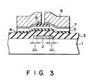
- the length of an overlapped region between the source/drain and the gate electrode 2 is AL.
- the region corresponding to AL is indispensable for ensuring stable contact between the contact layer 7 and the active layer 5.
- a photomask is manually aligned in an exposure apparatus, or mechanical auto-alignment is employed, as in a stepper exposure apparatus.
- the patterning precision varies depending on who operates the exposure apparatus.
- the alignment precision depends on mechanical operations, and the patterning precision is limited by the mechanical precision of the exposure apparatus.
- a liquid crystal display device using a TFT it is very difficult to carry out patterning alignment over the entire area.
- the object of the present invention is to provide a method of manufacturing a thin-film semiconductor device, wherein the number of photomasks employed can be reduced and a channel protection layer of a TFT or the like can be precisely aligned with a gate electrode.
- EP-A-338 766 discloses the fabrication of a thin film transistor on a transparent insulative substrate by forming an opaque metal gate electrode on the substrate, followed by an insulative film, then an active layer, then a channel protection layer and then a positive first resist; photolithographically exposing the first resist from the reverse face of the substrate using the gate electrode as a mask and then patterning the active layer in the same way.
- the invention provides a method as defined in Claim 1.
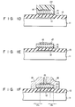
- Figs. 1A to 1F are cross-sectional views for illustrating a method of manufacturing a TFT according to a first embodiment of the present invention.
- Mo-Ta is deposited on a transparent insulative substrate 11 of, e. g. glass, by means of sputtering, thereby forming an opaque metal thin film on the substrate 11.
- the metal film is patterned by means of conventional lithography, thus forming a gate electrode 12.
- a lamination of, a silicon oxide film 13 and a silicon nitride film 14 is formed on the substrate 11 and the gate electrode 12 by means of plasma CVD.
- an amorphous silicon film is deposited as an active layer 15 by means of plasma CVD.
- a silicon nitride film is deposited as a channel protection layer 16.
- a first photoresist 21 of a positive type is coated on the silicon nitride film deposited as the channel protection layer 16, and the reverse side of the substrate 11 is exposed.
- the amount of exposure light is made sufficiently greater than that necessary for patterning (i.e. the amount of exposure light necessary for forming a resist pattern which is the same as the pattern of the gate electrode 12).
- the gate electrode 12 serves as a mask, and the resist 21 is selectively exposed.
- the amount of exposure light is excessive, and therefore the width of the developed resist pattern is less than that of the gate electrode 12 used as the mask, as shown in Fig. 1B.
- the silicon nitride film serving as channel protection layer 16 is selectively etched, so as to leave a selected portion of the channel protection layer 16 above the gate electrode 12.
- a second photoresist 22 of a positive type is coated once again, as shown in Fig. 1C, and the reverse side of the substrate 11 is exposed once again.
- the amount of exposure light is less than that of exposure light used for forming the channel protection layer 16.
- a contact layer 17 serving as a phosphor-doped amorphous silicon (n + a-Si) film is deposited, as shown in Fig. 1E.
- the amorphous silicon is patterned in an island shape with use of a photomask.
- unnecessary portions of the channel protection layer 16 are simultaneously etched.
- the etching in this case is carried out, for example, by a chemical dry etching (CDE) using a Freon gas.
- CDE chemical dry etching
- the channel protection layer 16 can be formed within the gate electrode 12 in a self-alignment manner, a length ⁇ L of an overlapped portion of the source/drain region and the gate electrode 12 can be set with high precision, and the length ⁇ L on one side can easily be made equal to the length ⁇ L on the other side.
Landscapes
- Thin Film Transistor (AREA)
Claims (5)
- Verfahren zur Herstellung eines Dünnschicht-Halbleiterbauteils auf einer ersten Hauptfläche eines durchsichtigen isolierenden Substrats (11), welches auch eine der ersten Hauptfläche gegenüberliegende zweite Hauptfläche aufweist, in folgenden Stufen:Ablagern eines opaken Metallfilms auf der ersten Hauptfläche des Substrats (11) und Mustergebung des opaken Metallfilms zur Bildung einer Gateelektrode (12);sukzessives Ausbilden eines isolierenden Films (13, 14), einer aktiven Halbleiterschicht (15) und einer Kanalschutzschicht (16) auf der ersten Hauptfläche des Substrats (11) und der Gateelektrode (12);Mustergebung der Kanalschutzschicht (16) auf photolitographischem Wege mit einem durch rückseitige Überbelichtung unter Verwendung der Gateelektrode (12) als Maske belichteten ersten Resist (21), undMustergebung der aktiven Halbleiterschicht (15) auf photolitographischem Wege mit einem durch rückseitige Belichtung belichteten zweiten Resist (22), wobei die Belichtungsmenge geringer ist als bei der Bemusterung der Kanalschutzschicht (16) unter Verwendung der Gateelektrode (12) als Maske, um die Breite der aktiven Halbleiterschicht (15) in der Kanalrichtung gegenüber derjenigen der Kanalschutzschicht (16) zu vergrößern,dadurch gekennzeichnet, daß der Isolierfilm ein Laminat aus zwei auf der Hauptfläche des Substrats (11) und der Gateelektrode (12) gebildeten Filmen, von denen der eine aus einem Siliciumoxidfilm (13) und der andere aus einem Siliciumnitridfilm (14) besteht, umfaßt.
- Verfahren nach Anspruch 1, wobei der Abstand AL zwischen einem Endteil der gemusterten aktiven Halbleiterschicht (15) und einem Endteil der gemusterten Kanalschutzschicht (16) auf 0,3 µm < ΔL < 3,0 µm eingestellt ist.
- Verfahren nach Anspruch 1, bei welchem zusätzlich bei der Mustergebung der Kanalschutzschicht folgende Stufen:Auftragen eines positiven ersten Resists (21) auf die Kanalschutzschicht (16);Aufstrahlen von Licht auf die zweite Hauptfläche des Substrats (11) und Belichten des ersten Resists (21) unter Verwendung der Gateelektrode (12) als Maske, um einen gemusterten Teil des ersten Resists (21), der kleiner ist als die Gateelektrode (12), zurückzulassen;Mustergebung der Kanalschutzschicht (16) unter Verwendung des ersten Resists (21) als Maske;und bei der Mustergebung der aktiven Halbleiterschicht (15) folgende Stufen:Entfernen des ersten Resists (21) und Auftragen eines positiven zweiten Resists (22) auf die aktive Halbleiterschicht (15) und die gemusterte Kanalschutzschicht (16);Aufstrahlen von Licht auf die zweite Hauptfläche des Substrats (11) und Belichten des zweiten Resists (22) unter Verwendung der Gateelektrode (12) als Maske, um einen gemusterten Teil des zweiten Resists (22), der größer ist als der gemusterte Teil des ersten Resists (21) zurückzulassen;Mustergebung der aktiven Halbleiterschicht (15) unter Verwendung des zweiten Resists (22) als Maske,und zusätzlich der zweite Resist (22) entfernt und auf der gemusterten aktiven Halbleiterschicht (15) eine Source/Drain-Elektrode (17) gebildet werdendurchgeführt werden.
- Verfahren nach Anspruch 3, wobei der Abstand AL zwischen einem Endteil des gemusterten Bereichs des ersten Resists (21) und einem Endteil des gemusterten Bereichs des zweiten Resists (22) auf 0,3 µm ≤ ΔL ≤ 3,0 µm eingestellt wird.
- Verfahren nach Anspruch 3 oder 4, wobei der erste Resist (21) durch Überbelichtung mit einer größeren Belichtungsmenge, als zur Bildung eines Resistmusters einer zum Gateelektrodenmuster gleichen Größe erforderlich ist, belichtet wird.
Applications Claiming Priority (2)
| Application Number | Priority Date | Filing Date | Title |
|---|---|---|---|
| JP81356/90 | 1990-03-30 | ||
| JP2081356A JP2938121B2 (ja) | 1990-03-30 | 1990-03-30 | 薄膜半導体装置の製造方法 |
Publications (2)
| Publication Number | Publication Date |
|---|---|
| EP0449404A1 EP0449404A1 (de) | 1991-10-02 |
| EP0449404B1 true EP0449404B1 (de) | 1997-12-03 |
Family
ID=13744076
Family Applications (1)
| Application Number | Title | Priority Date | Filing Date |
|---|---|---|---|
| EP91300609A Expired - Lifetime EP0449404B1 (de) | 1990-03-30 | 1991-01-28 | Verfahren zur Herstellung eines Dünnschicht-Halbleiterbauteils auf einem transparenten, isolierenden Substrat |
Country Status (3)
| Country | Link |
|---|---|
| EP (1) | EP0449404B1 (de) |
| JP (1) | JP2938121B2 (de) |
| DE (1) | DE69128295T2 (de) |
Cited By (1)
| Publication number | Priority date | Publication date | Assignee | Title |
|---|---|---|---|---|
| US7642584B2 (en) | 1991-09-25 | 2010-01-05 | Semiconductor Energy Laboratory Co., Ltd. | Semiconductor device and method for forming the same |
Families Citing this family (14)
| Publication number | Priority date | Publication date | Assignee | Title |
|---|---|---|---|---|
| US5306648A (en) * | 1986-01-24 | 1994-04-26 | Canon Kabushiki Kaisha | Method of making photoelectric conversion device |
| TW237562B (de) * | 1990-11-09 | 1995-01-01 | Semiconductor Energy Res Co Ltd | |
| JP3537854B2 (ja) * | 1992-12-29 | 2004-06-14 | エルジー フィリップス エルシーディー カンパニー リミテッド | 薄膜トランジスタの製造方法 |
| US5733804A (en) * | 1995-12-22 | 1998-03-31 | Xerox Corporation | Fabricating fully self-aligned amorphous silicon device |
| US5717223A (en) * | 1995-12-22 | 1998-02-10 | Xerox Corporation | Array with amorphous silicon TFTs in which channel leads overlap insulating region no more than maximum overlap |
| JP2001189461A (ja) * | 1999-10-21 | 2001-07-10 | Matsushita Electric Ind Co Ltd | 薄膜トランジスタ及びそれを用いた液晶表示装置 |
| JP4789915B2 (ja) * | 2000-08-28 | 2011-10-12 | シャープ株式会社 | アクティブマトリクス基板及びその製造方法 |
| GB2421115A (en) * | 2004-12-09 | 2006-06-14 | Seiko Epson Corp | A self-aligning patterning method for use in the manufacture of a plurality of thin film transistors |
| JP2007012652A (ja) * | 2005-06-28 | 2007-01-18 | Sony Corp | 薄膜トランジスタ基板および薄膜トランジスタ基板の製造方法 |
| US9401431B2 (en) * | 2009-04-21 | 2016-07-26 | Cbrite Inc. | Double self-aligned metal oxide TFT |
| CN102655095B (zh) * | 2011-06-01 | 2014-10-15 | 京东方科技集团股份有限公司 | 薄膜晶体管及阵列基板的制造方法 |
| JP5668696B2 (ja) * | 2012-01-13 | 2015-02-12 | ソニー株式会社 | 薄膜トランジスタ基板の製造方法 |
| CN116941028A (zh) * | 2023-05-11 | 2023-10-24 | 昆山龙腾光电股份有限公司 | 阵列基板的制作方法及阵列基板 |
| CN117440711A (zh) * | 2023-10-19 | 2024-01-23 | 惠科股份有限公司 | 阵列基板及其制备方法、显示装置 |
Family Cites Families (4)
| Publication number | Priority date | Publication date | Assignee | Title |
|---|---|---|---|---|
| FR2590406B1 (fr) * | 1985-11-15 | 1988-10-28 | Commissariat Energie Atomique | Procede de fabrication d'un transistor en couches minces a grille auto-alignee par rapport au drain et a la source de celui-ci |
| EP0270323B1 (de) * | 1986-11-29 | 1999-11-03 | Sharp Kabushiki Kaisha | Verfahren zur Herstellung eines Dünnschichttransistors |
| JPH01173650A (ja) * | 1987-12-26 | 1989-07-10 | Seikosha Co Ltd | 非晶質シリコン薄膜トランジスタの製造方法 |
| JPH0242761A (ja) * | 1988-04-20 | 1990-02-13 | Matsushita Electric Ind Co Ltd | アクティブマトリクス基板の製造方法 |
-
1990
- 1990-03-30 JP JP2081356A patent/JP2938121B2/ja not_active Expired - Fee Related
-
1991
- 1991-01-28 DE DE69128295T patent/DE69128295T2/de not_active Expired - Fee Related
- 1991-01-28 EP EP91300609A patent/EP0449404B1/de not_active Expired - Lifetime
Cited By (1)
| Publication number | Priority date | Publication date | Assignee | Title |
|---|---|---|---|---|
| US7642584B2 (en) | 1991-09-25 | 2010-01-05 | Semiconductor Energy Laboratory Co., Ltd. | Semiconductor device and method for forming the same |
Also Published As
| Publication number | Publication date |
|---|---|
| EP0449404A1 (de) | 1991-10-02 |
| JPH03283539A (ja) | 1991-12-13 |
| JP2938121B2 (ja) | 1999-08-23 |
| DE69128295T2 (de) | 1998-04-09 |
| DE69128295D1 (de) | 1998-01-15 |
Similar Documents
| Publication | Publication Date | Title |
|---|---|---|
| US5137841A (en) | Method of manufacturing a thin film transistor using positive and negative photoresists | |
| USRE41632E1 (en) | Liquid crystal display device and method of manufacturing the same | |
| EP0449404B1 (de) | Verfahren zur Herstellung eines Dünnschicht-Halbleiterbauteils auf einem transparenten, isolierenden Substrat | |
| US5441905A (en) | Process of making self-aligned amorphous-silicon thin film transistors | |
| JP2003297850A (ja) | 薄膜トランジスタアレイ及びその製造方法並びにこれを用いた液晶表示装置 | |
| US5166086A (en) | Thin film transistor array and method of manufacturing same | |
| JP2011023741A (ja) | アレイ | |
| KR100420547B1 (ko) | 프로세스 윈도우를 개선하여 완전하게 셀프 얼라인된 tft를 형성하는 방법 | |
| KR20020093351A (ko) | 그레이톤 마스크 및 이를 이용한 액정디스플레이 제조방법 | |
| US6391499B1 (en) | Light exposure mask and method of manufacturing the same | |
| US7312470B2 (en) | Thin film transistor array panel and method for fabricating the same | |
| JP2678044B2 (ja) | アクティブマトリクス基板の製造方法 | |
| KR20000059689A (ko) | 액정표시장치용박막트랜지스터기판의제조방법 | |
| US20050148123A1 (en) | Method for fabricating self-aligned thin-film transistor | |
| US6411356B1 (en) | Liquid crystal display device with an organic insulating layer having a uniform undamaged surface | |
| US6316295B1 (en) | Thin film transistor and its fabrication | |
| US6219114B1 (en) | Liquid crystal display device with reduced source/drain parasitic capacitance and method of fabricating same | |
| JP3093314B2 (ja) | 薄膜トランジスタ及びその製造方法 | |
| JPH0488641A (ja) | 薄膜トランジスタの製造方法 | |
| JP2854025B2 (ja) | 薄膜トランジスタの製造方法 | |
| US5889290A (en) | Thin film transistor and manufacturing method thereof | |
| JP2782829B2 (ja) | 薄膜トランジスタの製造方法 | |
| JPH04282839A (ja) | 薄膜トランジスタ及びその製造方法 | |
| KR100527080B1 (ko) | 박막 트랜지스터 어레이 기판의 제조방법 | |
| TW594349B (en) | Liquid crystal display device and method of the same |
Legal Events
| Date | Code | Title | Description |
|---|---|---|---|
| PUAI | Public reference made under article 153(3) epc to a published international application that has entered the european phase |
Free format text: ORIGINAL CODE: 0009012 |
|
| 17P | Request for examination filed |
Effective date: 19910222 |
|
| AK | Designated contracting states |
Kind code of ref document: A1 Designated state(s): DE FR GB |
|
| 17Q | First examination report despatched |
Effective date: 19940801 |
|
| GRAG | Despatch of communication of intention to grant |
Free format text: ORIGINAL CODE: EPIDOS AGRA |
|
| GRAH | Despatch of communication of intention to grant a patent |
Free format text: ORIGINAL CODE: EPIDOS IGRA |
|
| GRAH | Despatch of communication of intention to grant a patent |
Free format text: ORIGINAL CODE: EPIDOS IGRA |
|
| GRAA | (expected) grant |
Free format text: ORIGINAL CODE: 0009210 |
|
| AK | Designated contracting states |
Kind code of ref document: B1 Designated state(s): DE FR GB |
|
| REF | Corresponds to: |
Ref document number: 69128295 Country of ref document: DE Date of ref document: 19980115 |
|
| ET | Fr: translation filed | ||
| PLBE | No opposition filed within time limit |
Free format text: ORIGINAL CODE: 0009261 |
|
| STAA | Information on the status of an ep patent application or granted ep patent |
Free format text: STATUS: NO OPPOSITION FILED WITHIN TIME LIMIT |
|
| REG | Reference to a national code |
Ref country code: GB Ref legal event code: 746 Effective date: 19981002 |
|
| 26N | No opposition filed | ||
| REG | Reference to a national code |
Ref country code: FR Ref legal event code: D6 |
|
| REG | Reference to a national code |
Ref country code: GB Ref legal event code: IF02 |
|
| PGFP | Annual fee paid to national office [announced via postgrant information from national office to epo] |
Ref country code: GB Payment date: 20070124 Year of fee payment: 17 |
|
| PGFP | Annual fee paid to national office [announced via postgrant information from national office to epo] |
Ref country code: DE Payment date: 20070125 Year of fee payment: 17 |
|
| PGFP | Annual fee paid to national office [announced via postgrant information from national office to epo] |
Ref country code: FR Payment date: 20070109 Year of fee payment: 17 |
|
| GBPC | Gb: european patent ceased through non-payment of renewal fee |
Effective date: 20080128 |
|
| PG25 | Lapsed in a contracting state [announced via postgrant information from national office to epo] |
Ref country code: DE Free format text: LAPSE BECAUSE OF NON-PAYMENT OF DUE FEES Effective date: 20080801 |
|
| REG | Reference to a national code |
Ref country code: FR Ref legal event code: ST Effective date: 20081029 |
|
| PG25 | Lapsed in a contracting state [announced via postgrant information from national office to epo] |
Ref country code: GB Free format text: LAPSE BECAUSE OF NON-PAYMENT OF DUE FEES Effective date: 20080128 |
|
| PG25 | Lapsed in a contracting state [announced via postgrant information from national office to epo] |
Ref country code: FR Free format text: LAPSE BECAUSE OF NON-PAYMENT OF DUE FEES Effective date: 20080131 |