EP0449441A1 - Antisättigungsschaltkreis für einen bipolaren Transistor - Google Patents
Antisättigungsschaltkreis für einen bipolaren Transistor Download PDFInfo
- Publication number
- EP0449441A1 EP0449441A1 EP91301873A EP91301873A EP0449441A1 EP 0449441 A1 EP0449441 A1 EP 0449441A1 EP 91301873 A EP91301873 A EP 91301873A EP 91301873 A EP91301873 A EP 91301873A EP 0449441 A1 EP0449441 A1 EP 0449441A1
- Authority
- EP
- European Patent Office
- Prior art keywords
- transistor
- coupled
- collector
- input
- voltage
- Prior art date
- Legal status (The legal status is an assumption and is not a legal conclusion. Google has not performed a legal analysis and makes no representation as to the accuracy of the status listed.)
- Ceased
Links
- 239000003990 capacitor Substances 0.000 claims description 6
- 238000000034 method Methods 0.000 abstract description 11
- 230000007423 decrease Effects 0.000 description 8
- 230000008901 benefit Effects 0.000 description 3
- 238000012544 monitoring process Methods 0.000 description 3
- 230000002411 adverse Effects 0.000 description 2
- 238000013459 approach Methods 0.000 description 2
- 239000000969 carrier Substances 0.000 description 2
- 230000008859 change Effects 0.000 description 2
- 238000010586 diagram Methods 0.000 description 2
- 230000003071 parasitic effect Effects 0.000 description 2
- 230000009471 action Effects 0.000 description 1
- 230000010355 oscillation Effects 0.000 description 1
- 230000004044 response Effects 0.000 description 1
- 238000009738 saturating Methods 0.000 description 1
- 230000007704 transition Effects 0.000 description 1
Images

Classifications
-
- H—ELECTRICITY
- H03—ELECTRONIC CIRCUITRY
- H03K—PULSE TECHNIQUE
- H03K17/00—Electronic switching or gating, i.e. not by contact-making and –breaking
- H03K17/04—Modifications for accelerating switching
- H03K17/042—Modifications for accelerating switching by feedback from the output circuit to the control circuit
- H03K17/0422—Anti-saturation measures
-
- G—PHYSICS
- G05—CONTROLLING; REGULATING
- G05F—SYSTEMS FOR REGULATING ELECTRIC OR MAGNETIC VARIABLES
- G05F3/00—Non-retroactive systems for regulating electric variables by using an uncontrolled element, or an uncontrolled combination of elements, such element or such combination having self-regulating properties
- G05F3/02—Regulating voltage or current
- G05F3/08—Regulating voltage or current wherein the variable is DC
- G05F3/10—Regulating voltage or current wherein the variable is DC using uncontrolled devices with non-linear characteristics
- G05F3/16—Regulating voltage or current wherein the variable is DC using uncontrolled devices with non-linear characteristics being semiconductor devices
- G05F3/20—Regulating voltage or current wherein the variable is DC using uncontrolled devices with non-linear characteristics being semiconductor devices using diode- transistor combinations
- G05F3/22—Regulating voltage or current wherein the variable is DC using uncontrolled devices with non-linear characteristics being semiconductor devices using diode- transistor combinations wherein the transistors are of the bipolar type only
- G05F3/222—Regulating voltage or current wherein the variable is DC using uncontrolled devices with non-linear characteristics being semiconductor devices using diode- transistor combinations wherein the transistors are of the bipolar type only with compensation for device parameters, e.g. Early effect, gain, manufacturing process, or external variations, e.g. temperature, loading, supply voltage
Definitions
- the present invention relates generally to the field of electronic circuits and more particularly, to electronic circuits having antisaturation protection.
- Bipolar transistors exhibit the characteristics of a switch when driven to the extreme conditions of cut-off and saturation mode.
- the advantages of driving a transistor into saturation mode include a low voltage across collector and emitter inputs known as a saturation voltage (V CESAT ), and a low collector-emitter resistance, which provides for optimum efficiency.
- V CESAT saturation voltage
- I C collector current
- I C collector current
- I C collector-emitter voltage
- a bipolar transistor driven into deep saturation causes minority carriers from its collector to be injected into its base.
- the turn off time of the transistor is adversely affected and becomes a function of the transistor's storage time (t s ) since the minority carriers must be swept. out of the base before the transistor is turned off.
- Switching speed of bipolar transistors is a major advantage and numerous techniques have been employed to keep transistors out of saturation mode and/or deep saturation mode for improved turn off times.
- a common antisaturation technique comprises shunting a collector-base junction of a NPN transistor with a Schottky diode.
- the Schottky diode exhibits a lower forward voltage (V F ) than the forward biased collector-base junction and thus clamps the junction at the lower voltage, therein preventing the transistor from operating in the saturation mode.
- V F forward voltage
- the V F of tine Schottky diode changes with temperature at a rate equal to approximately one half the rate of change of the transistor's collector-base voltage with temperature.
- An aim of the present invention is to provide an antisaturation circuit that keeps a transistor out of saturation without stealing current from the base of the transistor.
- an antisaturation circuit comprising: detecting means having a first input coupled to a first input of the protected transistor and a second input coupled to a second input of the protected transistor for detecting a voltage therebetween; a first current source coupled to the detecting means for providing a first substantially constant current to the detecting means; and a second current source coupled to the detecting means and the protected transistor for providing a second substantially constant current apportioned between the detecting means and the protected transistor according to the detected voltage to prevent the protected transistor from operating in a saturation mode.
- this provides an antisaturation circuit of the present invention that is useful for analog applications.
- an antisaturation circuit for controlling a protected transistor, the antisaturation circuit comprising: detecting means having a first input coupled to a first input of the protected transistor and a second input coupled to a second input of the protected transistor for monitoring a voltage therebetween; first current means coupled to the detecting means for providing a first substantially constant current to the detecting means; and second current means coupled to the detecting means and the protected transistor for providing a second substantially constant current thereto, wherein the second substantially constant current is apportioned between the differential input means and the protected transistor according to the detected voltage to prevent the protected transistor from operating in a saturation mode.
- the antisaturation circuit of the present invention thus monitors the voltage of the transistor to be protected.
- a detecting circuit having first and second inputs coupled to first and second inputs of a protected transistor to be kept out of saturation mode and monitoring a voltage of the protected transistor that is indicative of an on-coming saturation mode.
- a first current source is coupled to the detecting circuit for supplying a constant current thereto.
- a second current source is coupled to both the detecting circuit and the protected transistor which allows a portion of a current, other than the base current, of the protected transistor to be diverted to the detecting circuit according to the monitored voltage to ensure the protected transistor does not operate in the saturation mode.
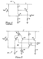
- FIG. 1 is a schematic representation of a prior art unity gain buffer circuit.
- FIG. 2 is a schematic representation of a voltage buffer having an improved antisaturation circuit.
- FIG. 3 is a schematic representation of second embodiment of a voltage buffer having an improved antisaturation circuit.
- FIG. 4 is a block diagram of a peak follower comprising a voltage buffer circuit.
- FIG. 5 is a block diagram of a DC restore circuit comprising a voltage buffer circuit.
- a unity gain buffer circuit 10 useful for low frequency applications and having a limited voltage range is shown in FIG. 1.
- a transistor 9 of the unity gain buffer circuit 10 will typically switch into and out of saturation mode when used in non-linear applications or when a slew rate of an input voltaqe is too fast.
- the transistor 9 goes into saturation mode, its turn-off time increases, thus causing the unity gain buffer circuit 10 to require additional time to settle (settling time) after a fast slew.
- settling time settling time
- a response time and hence the effective bandwidth
- Saturation mode operation of the transistor 9 also creates an undesirable offset from an input terminal 3 to an output terminal 17. The offset is a difference in magnitude between the input voltage and an output voltage. If the transistor 9 is prevented from operating in the saturation mode, both the settling time and effective bandwidth of the unity gain buffer 10 could be improved making it useful in higher performance applications.
- a voltage buffer circuit 20, shown in FIG. 2 is made up of a unity gain buffer circuit similar to the unity gain buffer circuit 10 shown in FIG. 1 and an antisaturation circuit 30. Devices similar to those used in FIG. 1 and repeated in FIG. 2 are represented by primed numbers.
- the voltage buffer circuit 20 includes an input transistor 5′ having a base connected to an input terminal 3′, its collector input connected to a supply voltage terminal 1′, and its emitter input connected to an emitter input of a transistor 9′.
- the transistor 9′ has its collector input coupled to the supply voltage terminal 1′ through a resistor 7′ for receiving a positive supply voltage, and its base input coupled to a supply voltage terminal 2′ through a resistor 15′.
- An output transistor 13′ has its collector input connected to the supply voltage terminal 1′, its base input connected to the collector input of the transistor 9′, and its emitter input connected to an output terminal 17′ and to the base input of the transistor 9′.
- the resistor 7′, the transistor 13′, and the resistor 15′ provide the output driving function for the buffer circuit 20.
- the antisaturation circuit 30 includes transistors 21 and 23 having their emitter inputs, forming first and second inputs, respectively, of the antisaturation circuit, are coupled to the supply voltage terminal 1′ by a current source 19, and their base inputs, forming first and second inputs, respectively of the antisaturation circuit, are connected to the base and collector inputs, respectively, of the transistor 9′.
- a collector input of the transistor 21 is connected to the supply voltage terminal 2′.
- a collector input of the transistor 23 is connected to the emitter input of the transistor 9' and the supply voltage terminal 2′ by a current source 25.
- the transistors 21 and 23 form an emitter-coupled pair of a detecting circuit which is used to monitor and amplify a collector-base voltage of the transistor 9′. If a collector-base junction of the transistor 9′ becomes forward biased, the transistor 9′ would go into the saturation mode.
- the antisaturation circuit 30 prevents this from occurring as described below.
- the voltage buffer circuit 20 When an input voltage (V IN ) at the input terminal 3′ is in a steady-state, the voltage buffer circuit 20 operates so that an output voltage (V OUT ) at the output terminal 17′ is substantially equal to V IN plus an offset voltage.
- the offset voltage is the difference between V IN and V OUT and is the result of different biases and base-emitter voltages (V BE ) of the transistors 5′ and 9′.
- the transistor 13′ In an equilibrium state, the transistor 13′ is biased in a conducting state and the magnitude of the voltage at the bases of the transistors 13′ and 23 is substantially equal to the magnitude of the voltage at the bases of the transistors 9′ and 21 plus a V BE . As a result, the transistor 23 is in an off state.
- the buffer circuit 20 would not be able to track the change instantaneously due to slew rate limiting factors such as parasitic capacitances of the transistors 9′ and 13′, any external load capacitance at the output terminal 17′, and the limited bandwidth of all the transistors.
- the transistor 5′ will be in an off state and the transistor 9′ will conduct more current until the output voltage V OUT can slew to within 3V T of V IN , wherein V T is 25.8 millivolts at room temperature.
- the resistor 7′ will carry the additional current that the transistor 9′ conducts causing the magnitude of the voltage at the bases of the transistors 13′ and 23 to decrease, thereby turning off the transistor 13′.
- the transistor 9′ approaches the saturation mode as the voltage at its collector approaches the voltage at its base. However, saturation mode is avoided because the transistor 23 begins to conduct a portion of a current I1 from the current source 19 into the emitter of the transistor 9′ which essentially reduces the emitter and collector current bias of the transistor 9′. Thereafter a new equilibrium is reached wherein the antisaturation circuit 30 acts to adjust the current bias of the transistor 9′ such that the saturation mode is avoided.
- the current I1 is greater than or equal to a current I2 from the current source 25 and the V CESAT of the transistor 9′ is less than V BE - 4V T , where V BE is the base-emitter voltage.
- the transistor 9′ is thus protected from going into saturation mode without stealing its base current therein making the antisaturation circuit 30 useful for both linear and non-linear operations.
- An alternative embodiment such as voltage buffer circuit 40, is shown in FIG. 3. Numbers used in FIG. 1 are repeated in FIG. 3 with double primes to represent like devices.
- the voltage buffer circuit 40 includes an input transistor 5 ⁇ having a collector input connected to a supply voltage terminal 1 ⁇ , a base input connected to an input terminal 3 ⁇ for receiving an input voltage, V IN , and an emitter input coupled to a supply voltage terminal 2 ⁇ by a current source 37.
- a transistor 33 connected to function as a diode, has collector and base inputs coupled to the supply voltage termimal 1 ⁇ by a current source 39, and its emitter input coupled to the supply voltage terminal 2 ⁇ by a current source 35.
- a transistor 31 has its collector input connected to the supply voltage terminal 1 ⁇ , its base input connected to an output terminal 17 ⁇ , and its emitter input coupled to the supply voltage terminal 2 ⁇ by the current source 35.
- Transistor 9 ⁇ is the transistor that is protected from going into the saturation mode. The speed of the voltage buffer circuit 40 is increased because transistor 9 ⁇ is kept in a forward linear region of operation at all times.
- Transistor 9 ⁇ has its collector input connected to the collector input of the transistor 33, its base input connected to the output terminal 17 ⁇ , and its emitter input coupled to the supply voltage terminal 2 ⁇ by the current source 37.
- Transistor 13 has its collector input connected to the supply voltage terminal 1 ⁇ , its base input connected to the collector of the transistor 9 ⁇ , and its emitter input connected to the output terminal 17 ⁇ and the supply voltage terminal 2 ⁇ by a resistor 15 ⁇ .
- the transistor 13 ⁇ , the resistor 15 ⁇ , and the current source 39 provide the output driving function for the voltage buffer circuit 40.
- the transistors 31, and 33 in combination with the current source 35, form a differential amplifier, or detecting circuit with bases providing first and second inputs respectively, wherein the sum of the currents flowing through the transistors 31 and 33 equals a current I3 flowing in the current source 35.
- a current I2′ flowing in the current source 37 is set, for example, substantially equal to I3, and a current I1′ flowing in the current source 39 is set to substantially equal 1.5 times I2′.
- the transistors 5 ⁇ and 9 ⁇ are matched transistors, and the current I1′ is set to be less than the sum of the currents I2′ and I3.
- V IN is substantially equal to the magnitude of V OUT and the sum of the currents flowing through the transistors 5 ⁇ and 9 ⁇ is substantially equal to I2′.
- V OUT exceeds V IN
- the current flowing in the transistor 9 ⁇ begins to increase above I2′/2 causing its collector voltage (V A ) to decrease towards V OUT .
- V A collector voltage
- This decrease causes the current in the transistor 31 to increase and the current in the transistor 33 to decrease until equilibrium is reached thus circumventing the saturation mode of operation of the transistor 9 ⁇ .
- the voltage buffer circuit 20 (FIG. 2), and the voltage buffer circuit 40 may be used in a variety of applications.
- An example of using the voltage buffer circuits 20 and 40 as a peak follower 60 is shown in FIG. 4.
- a voltage buffer 61 has an input terminal 3′′′ connected for receiving an input voltage, V IN , and an output terminal 17′′′ connected for providing an output voltage, V OUT .
- the voltage buffer 61 is equivalent to either the voltage buffer circuit 20 or the voltage buffer circuit 40, each of which have the resistor 15′ or 15 ⁇ , respectively, replaced by a capacitor 63.
- the voltage buffer circuit 61 is able to function as a peak detector because a base current of the respective transistor 9′ or 9 ⁇ is the only current available to discharge the capacitor 63 once it is charged and, as already described, the base current of the transistor 9′ or 9 ⁇ is not changed substantially when keeping the transistor 9′ or 9 ⁇ out of the saturation mode.
- a DC restore circuit 70 is shown in FIG. 5.
- the restore circuit 70 is similar to the peak follower 60 with the exception that V IN performs the function of a bias voltage, and an AC signal source 71 is coupled between the supply voltage terminal 2′′′′ and a capacitor 63′ for providing an AC signal.
- the AC signal drives the output voltage, V OUT , through the capacitor 63′.
- V OUT will equal the value of the AC signal plus a DC component.
- the most negative magnitude of V OUT will substantially equal the bias voltage V IN .
- the performance of both linear and non-linear circuits may be substantially improved by the use of antisaturation circuits as described herein.
- This technique protects a transistor from operating in both the deep saturation mode and the saturation mode.
- the antisaturation circuit accomplishes antisaturation protection by monitoring the protected transistor's collector-base voltage and thus uses voltage feedback to signify the potential of saturation mode operation. When the oncoming saturation mode is detected, the collector current of the protected transistor is reduced thus keeping the protected transistor from saturating. Reducing the collector current based on the collector-base voltage of the protected transistor rather than using the typical techniques of steering the base current into the collector has the advantage of keeping the protected transistors input impedance substantially unchanged.
- the resistor 7′ or 7 ⁇ of FIG. 2 or 3, respectively could be replaced by a current source similar to the current source 19 to improve accuracy of the circuit.
- the current source 39 of FIG. 3 could be replaced by a resistor in order to reduce the number of devices.
- current mirrors could be used in the collectors or emitters of the active devices to improve the circuit's performance.
- base resistors may be inserted at the bases of the transistor to reduce the possibility of unwanted circuit oscillations.
Landscapes
- Engineering & Computer Science (AREA)
- Microelectronics & Electronic Packaging (AREA)
- Physics & Mathematics (AREA)
- Nonlinear Science (AREA)
- Electromagnetism (AREA)
- General Physics & Mathematics (AREA)
- Radar, Positioning & Navigation (AREA)
- Automation & Control Theory (AREA)
- Amplifiers (AREA)
- Electronic Switches (AREA)
Applications Claiming Priority (2)
| Application Number | Priority Date | Filing Date | Title |
|---|---|---|---|
| US496752 | 1990-03-21 | ||
| US07/496,752 US5036218A (en) | 1990-03-21 | 1990-03-21 | Antisaturation circuit |
Publications (1)
| Publication Number | Publication Date |
|---|---|
| EP0449441A1 true EP0449441A1 (de) | 1991-10-02 |
Family
ID=23973974
Family Applications (1)
| Application Number | Title | Priority Date | Filing Date |
|---|---|---|---|
| EP91301873A Ceased EP0449441A1 (de) | 1990-03-21 | 1991-03-06 | Antisättigungsschaltkreis für einen bipolaren Transistor |
Country Status (3)
| Country | Link |
|---|---|
| US (1) | US5036218A (de) |
| EP (1) | EP0449441A1 (de) |
| JP (1) | JPH04347924A (de) |
Families Citing this family (4)
| Publication number | Priority date | Publication date | Assignee | Title |
|---|---|---|---|---|
| JP3526484B2 (ja) * | 1995-04-12 | 2004-05-17 | 日本テキサス・インスツルメンツ株式会社 | 高入力インピーダンス回路 |
| US6194910B1 (en) | 1998-06-24 | 2001-02-27 | Teradyne, Inc. | Relayless voltage measurement in automatic test equipment |
| US6580308B1 (en) * | 2002-06-27 | 2003-06-17 | Texas Instruments Incorporated | VDS protection for high voltage swing applications |
| US7994858B2 (en) * | 2009-05-15 | 2011-08-09 | Altasens, Inc. | Operational trans-conductance amplifier with output clamp circuit |
Citations (7)
| Publication number | Priority date | Publication date | Assignee | Title |
|---|---|---|---|---|
| US4021687A (en) * | 1974-11-06 | 1977-05-03 | Hitachi, Ltd. | Transistor circuit for deep saturation prevention |
| DE3619346A1 (de) * | 1985-06-24 | 1987-01-02 | Sgs Microelettronica Spa | Antisaettigungs-schaltung fuer einen integrierten pnp-transistor |
| DE3626817A1 (de) * | 1985-08-09 | 1987-02-12 | Sgs Microelettronica Spa | Antisaettigungsschaltung fuer einen integrierten pnp-transistor mit einer gemaess einer voreingestellten funktion definierbaren interventionscharakteristik |
| US4675548A (en) * | 1984-11-13 | 1987-06-23 | Harris Corporation | Antisaturation circuit for TTL circuits having TTL input and output compatibility |
| EP0241785A2 (de) * | 1986-03-31 | 1987-10-21 | Kabushiki Kaisha Toshiba | Ausgangstreiberschaltung |
| EP0161973B1 (de) * | 1984-04-19 | 1987-11-19 | Thomson-Csf | Vergleicher mit Verriegelungsschaltung und Analog-Digital-Wandler unter Benutzung solcher Vergleicher |
| DD256967A1 (de) * | 1986-12-31 | 1988-05-25 | Akad Wissenschaften Ddr | Antisaettigungsschaltung fuer leistungsschalttransistoren |
Family Cites Families (9)
| Publication number | Priority date | Publication date | Assignee | Title |
|---|---|---|---|---|
| US4338646A (en) * | 1981-04-27 | 1982-07-06 | Motorola, Inc. | Current limiting circuit |
| JPS60172816A (ja) * | 1984-02-17 | 1985-09-06 | Fuji Electric Co Ltd | トランジスタ駆動制御回路 |
| FR2579844B1 (fr) * | 1985-04-02 | 1987-05-15 | Thomson Csf | Circuit de commande de base de transistor fonctionnant a frequence elevee |
| US4710793A (en) * | 1985-09-04 | 1987-12-01 | Motorola, Inc. | Voltage comparator with hysteresis |
| US4755741A (en) * | 1986-11-18 | 1988-07-05 | Linear Technology Corporation | Adaptive transistor drive circuit |
| JPH01236806A (ja) * | 1988-03-17 | 1989-09-21 | Matsushita Electric Ind Co Ltd | 電圧フォロワ回路 |
| US4914320A (en) * | 1988-07-27 | 1990-04-03 | Unisys Corporation | Speed-up circuit for NPN bipolar transistors |
| US4980578A (en) * | 1988-12-20 | 1990-12-25 | Texas Instruments Incorporated | Fast sense amplifier |
| US4988899A (en) * | 1989-05-15 | 1991-01-29 | National Semiconductor Corporation | TTL gate current source controlled overdrive and clamp circuit |
-
1990
- 1990-03-21 US US07/496,752 patent/US5036218A/en not_active Expired - Fee Related
-
1991
- 1991-02-15 JP JP3042184A patent/JPH04347924A/ja active Pending
- 1991-03-06 EP EP91301873A patent/EP0449441A1/de not_active Ceased
Patent Citations (7)
| Publication number | Priority date | Publication date | Assignee | Title |
|---|---|---|---|---|
| US4021687A (en) * | 1974-11-06 | 1977-05-03 | Hitachi, Ltd. | Transistor circuit for deep saturation prevention |
| EP0161973B1 (de) * | 1984-04-19 | 1987-11-19 | Thomson-Csf | Vergleicher mit Verriegelungsschaltung und Analog-Digital-Wandler unter Benutzung solcher Vergleicher |
| US4675548A (en) * | 1984-11-13 | 1987-06-23 | Harris Corporation | Antisaturation circuit for TTL circuits having TTL input and output compatibility |
| DE3619346A1 (de) * | 1985-06-24 | 1987-01-02 | Sgs Microelettronica Spa | Antisaettigungs-schaltung fuer einen integrierten pnp-transistor |
| DE3626817A1 (de) * | 1985-08-09 | 1987-02-12 | Sgs Microelettronica Spa | Antisaettigungsschaltung fuer einen integrierten pnp-transistor mit einer gemaess einer voreingestellten funktion definierbaren interventionscharakteristik |
| EP0241785A2 (de) * | 1986-03-31 | 1987-10-21 | Kabushiki Kaisha Toshiba | Ausgangstreiberschaltung |
| DD256967A1 (de) * | 1986-12-31 | 1988-05-25 | Akad Wissenschaften Ddr | Antisaettigungsschaltung fuer leistungsschalttransistoren |
Also Published As
| Publication number | Publication date |
|---|---|
| US5036218A (en) | 1991-07-30 |
| JPH04347924A (ja) | 1992-12-03 |
Similar Documents
| Publication | Publication Date | Title |
|---|---|---|
| US5552746A (en) | Gate drive circuit | |
| US4887181A (en) | Circuit for temperature protection with hysteresis | |
| CN112003595B (zh) | 用于并联的开关晶体管的米勒钳位装置及包括其的驱动器 | |
| US4855618A (en) | MOS current mirror with high output impedance and compliance | |
| US2949543A (en) | Electronic amplifier | |
| EP0189564B1 (de) | Schaltung zur Beschleunigung des Hoch-Tief-Überganges für TTL-Gatter | |
| US5036218A (en) | Antisaturation circuit | |
| US4922208A (en) | Output stage for an operational amplifier | |
| US3924158A (en) | Electronic overload protection device | |
| US6114904A (en) | Fast amplifier output stage | |
| US5105145A (en) | Voltage control circuit | |
| US4645999A (en) | Current mirror transient speed up circuit | |
| EP0580921B1 (de) | Sättigungssteuerung eines integrierten bipolaren Transistors | |
| CN118012220B (zh) | 一种基于威尔逊电流镜的SiC MOSFET有源栅极驱动电路 | |
| WO1983004351A1 (en) | Current limiter and method for limiting current | |
| US6181496B1 (en) | Magnetic recording control circuit with voltage clamps | |
| US5055711A (en) | Impedance control circuit for an integrated circuit node | |
| US4675548A (en) | Antisaturation circuit for TTL circuits having TTL input and output compatibility | |
| US3609398A (en) | High-speed integrated logic circuit | |
| US3978349A (en) | Switching circuit | |
| US4409560A (en) | Output transient suppression circuit | |
| US4451747A (en) | High speed clamp circuit | |
| US5869995A (en) | Output stage having a high disabled output impedance and a low power integrated back buffer to provide disabled output device protection | |
| CN217037142U (zh) | 一种放大器电路与电子设备 | |
| US5903425A (en) | Lateral PNP fast turn-off circuit |
Legal Events
| Date | Code | Title | Description |
|---|---|---|---|
| PUAI | Public reference made under article 153(3) epc to a published international application that has entered the european phase |
Free format text: ORIGINAL CODE: 0009012 |
|
| AK | Designated contracting states |
Kind code of ref document: A1 Designated state(s): DE FR GB |
|
| 17P | Request for examination filed |
Effective date: 19911219 |
|
| 17Q | First examination report despatched |
Effective date: 19941227 |
|
| STAA | Information on the status of an ep patent application or granted ep patent |
Free format text: STATUS: THE APPLICATION HAS BEEN REFUSED |
|
| 18R | Application refused |
Effective date: 19960311 |