EP0450376B1 - Dispositif BiCMOS ayant des contacts peu espacés et procédé de fabrication - Google Patents
Dispositif BiCMOS ayant des contacts peu espacés et procédé de fabrication Download PDFInfo
- Publication number
- EP0450376B1 EP0450376B1 EP91104090A EP91104090A EP0450376B1 EP 0450376 B1 EP0450376 B1 EP 0450376B1 EP 91104090 A EP91104090 A EP 91104090A EP 91104090 A EP91104090 A EP 91104090A EP 0450376 B1 EP0450376 B1 EP 0450376B1
- Authority
- EP
- European Patent Office
- Prior art keywords
- polysilicon
- layer
- substrate
- region
- polysilicon layer
- Prior art date
- Legal status (The legal status is an assumption and is not a legal conclusion. Google has not performed a legal analysis and makes no representation as to the accuracy of the status listed.)
- Expired - Lifetime
Links
Images




Classifications
-
- H—ELECTRICITY
- H10—SEMICONDUCTOR DEVICES; ELECTRIC SOLID-STATE DEVICES NOT OTHERWISE PROVIDED FOR
- H10D—INORGANIC ELECTRIC SEMICONDUCTOR DEVICES
- H10D30/00—Field-effect transistors [FET]
- H10D30/01—Manufacture or treatment
- H10D30/021—Manufacture or treatment of FETs having insulated gates [IGFET]
- H10D30/0212—Manufacture or treatment of FETs having insulated gates [IGFET] using self-aligned silicidation
-
- H—ELECTRICITY
- H10—SEMICONDUCTOR DEVICES; ELECTRIC SOLID-STATE DEVICES NOT OTHERWISE PROVIDED FOR
- H10D—INORGANIC ELECTRIC SEMICONDUCTOR DEVICES
- H10D64/00—Electrodes of devices having potential barriers
- H10D64/01—Manufacture or treatment
- H10D64/011—Manufacture or treatment of electrodes ohmically coupled to a semiconductor
- H10D64/0111—Manufacture or treatment of electrodes ohmically coupled to a semiconductor to Group IV semiconductors
- H10D64/0113—Manufacture or treatment of electrodes ohmically coupled to a semiconductor to Group IV semiconductors the conductive layers comprising highly doped semiconductor materials, e.g. polysilicon layers or amorphous silicon layers
-
- H—ELECTRICITY
- H10—SEMICONDUCTOR DEVICES; ELECTRIC SOLID-STATE DEVICES NOT OTHERWISE PROVIDED FOR
- H10D—INORGANIC ELECTRIC SEMICONDUCTOR DEVICES
- H10D84/00—Integrated devices formed in or on semiconductor substrates that comprise only semiconducting layers, e.g. on Si wafers or on GaAs-on-Si wafers
- H10D84/01—Manufacture or treatment
- H10D84/0107—Integrating at least one component covered by H10D12/00 or H10D30/00 with at least one component covered by H10D8/00, H10D10/00 or H10D18/00, e.g. integrating IGFETs with BJTs
- H10D84/0109—Integrating at least one component covered by H10D12/00 or H10D30/00 with at least one component covered by H10D8/00, H10D10/00 or H10D18/00, e.g. integrating IGFETs with BJTs the at least one component covered by H10D12/00 or H10D30/00 being a MOS device
-
- H—ELECTRICITY
- H10—SEMICONDUCTOR DEVICES; ELECTRIC SOLID-STATE DEVICES NOT OTHERWISE PROVIDED FOR
- H10D—INORGANIC ELECTRIC SEMICONDUCTOR DEVICES
- H10D84/00—Integrated devices formed in or on semiconductor substrates that comprise only semiconducting layers, e.g. on Si wafers or on GaAs-on-Si wafers
- H10D84/01—Manufacture or treatment
- H10D84/02—Manufacture or treatment characterised by using material-based technologies
- H10D84/03—Manufacture or treatment characterised by using material-based technologies using Group IV technology, e.g. silicon technology or silicon-carbide [SiC] technology
- H10D84/038—Manufacture or treatment characterised by using material-based technologies using Group IV technology, e.g. silicon technology or silicon-carbide [SiC] technology using silicon technology, e.g. SiGe
-
- H—ELECTRICITY
- H10—SEMICONDUCTOR DEVICES; ELECTRIC SOLID-STATE DEVICES NOT OTHERWISE PROVIDED FOR
- H10D—INORGANIC ELECTRIC SEMICONDUCTOR DEVICES
- H10D84/00—Integrated devices formed in or on semiconductor substrates that comprise only semiconducting layers, e.g. on Si wafers or on GaAs-on-Si wafers
- H10D84/40—Integrated devices formed in or on semiconductor substrates that comprise only semiconducting layers, e.g. on Si wafers or on GaAs-on-Si wafers characterised by the integration of at least one component covered by groups H10D12/00 or H10D30/00 with at least one component covered by groups H10D10/00 or H10D18/00, e.g. integration of IGFETs with BJTs
- H10D84/401—Combinations of FETs or IGBTs with BJTs
-
- H—ELECTRICITY
- H10—SEMICONDUCTOR DEVICES; ELECTRIC SOLID-STATE DEVICES NOT OTHERWISE PROVIDED FOR
- H10D—INORGANIC ELECTRIC SEMICONDUCTOR DEVICES
- H10D64/00—Electrodes of devices having potential barriers
- H10D64/01—Manufacture or treatment
- H10D64/017—Manufacture or treatment using dummy gates in processes wherein at least parts of the final gates are self-aligned to the dummy gates, i.e. replacement gate processes
Definitions
- the present invention relates to the field of semiconductor devices and their manufacture. More specifically, in one embodiment the invention provides a process for both bipolar and complementary metal-oxide (CMOS) semiconductor devices on a single substrate.
- CMOS complementary metal-oxide
- BiCMOS devices offer the advantages of the high packing density and low power consumption of CMOS devices, as well as the high speed of bipolar devices.
- One BiCMOS device and process for fabrication thereof is described in U.S. Patent No. 4,764,480 (Vora), assigned to the assignee of the present invention.
- BiCMOS devices While meeting with some success, BiCMOS devices continue to have certain limitations. For example, electrical contacts in BiCMOS devices have caused limitations in their use. One limitation is the current drive capability of CMOS devices which is typically limited by source/drain sheet resistance. Extrinsic base resistance in bipolar transistors is in some instances an important factor in AC performance of bipolar structures. Still further, collector-substrate junction capacitance degrades the speed of bipolar circuits. High resistivity of a polysilicon-silicon substrate contact can limit the performance of especially small devices (e.g., sub-micron). Further, source and drain contacts in previous devices were spaced an undesirable distance from the gate of MOS transistors. T.-Y. Chiv et al. published in IEDM Technical Digest (1987) pages 24-27 a super self-aligned BICMOS structure. Also, ground tap resistance may be a limiting factor in removal of injected current from the substrate in vertical fuse devices.
- an improved BiCMOS device and method of fabrication thereof is desired not only to provide devices with improved performance and reduced size, but also to provide devices which can be fabricated more quickly and economically.
- the invention provides a method for forming a transistor structure as defined in the claims.
- the formed devices have improved performance, reduced size, and/or may be fabricated more quickly and economically.
- the source and drain contacts in MOS or CMOS devices extend fully up to gate sidewalls, so that only the gate sidewall thickness separates the source and drain contacts from the gate contact.
- the base contacts extend fully up to the emitter sidewall oxide.
- the process enables the formation of about 0.8 »m or smaller design rule CMOS and bipolar transistors.
- the devices may be used with, for example, high performance Emitter Coupled Logic (ECL) standard cell designs, memory cells, gate array designs with embedded memory, and the like.
- ECL Emitter Coupled Logic
- Fig. 1 illustrates a BiCMOS device in cross-section.
- the device includes a bipolar transistor 2 (which in the embodiment shown in Fig. 1 is an NPN transistor), an n-channel MOSFET (NMOS transistor) 4 and a p-channel MOSFET (PMOS transistor) 6.
- the devices are fabricated on a substrate 10 which includes a single-crystal body 10a and an epitaxial layer 11.
- the single-crystal body is a p- conductivity body having a dopant concentration of between about 1x10¹³ and 1x10¹⁶ atoms per cubic centimeter.
- a reduced pressure n-type epitaxial silicon layer 11 of desired thickness is grown on top of the single-crystal body.
- the devices are fabricated in the epitaxial layer 11 as described below.
- the NMOS transistor 4 is formed in a p+ tub or well 12 and the PMOS transistor 6 is formed in an n+ tub or well 14.
- the n+ well 14 is doped to a concentration of between about 1x1616 and 2x10²⁰/cm3
- the p+ well 12 is doped to a concentration of between about 1x10¹⁶ and 1x10¹⁸/cm3, although a wide range of dopant concentrations may be used without departing from the scope of the invention.
- Wells 12 and 14 enable the complementary conductivity devices to be formed on a single substrate.
- the NPN transistor 2 is provided with a heavily doped buried layer 16 and collector sink 17, which together provide a low resistance connection region between a collector contact 20e and the collector 16a beneath a p-type base 18.
- the buried layer 16 and sink 17 are doped to a concentration of between about 1x10¹⁷ and 1x10²⁰ with arsenic, antimony or the like, with a preferred range of about 5x10¹⁸ to 1x10²⁰/cm3.
- the collector 16a is a more lightly doped n-type formed between the base region 18 and the buried layer 16.
- An emitter region 27a is diffused from the emitter contact 27 into the underlying epitaxial layer 11.
- the NMOS device 4 and PMOS device 6 include regions which are formed in the epitaxial silicon region 11.
- the NMOS device 4 there are two self-aligned n type regions 20a, 20b that serve as the source and drain regions of the NMOS device.
- the PMOS device 6 there are two self-aligned p type implanted regions 20c, 20d that serve as the source and drain regions of the PMOS device.
- P+ channel stops 19, 19′ are provided between the transistors and adjacent devices to prevent leakage which would short circuit the buried layer 16 or well 14 with adjacent devices.
- oxide isolation regions 22a, 22b, 22c, 22d, and 22e, respectively are provided for device isolation which typically will be SiO2. Viewed from the top of the structure, these oxide isolation regions connect to each other to form annular bands around the active device areas.
- polycrystalline silicon (polysilicon) regions forming a resistor 24, p+ base contact 26, a portion of which 26′ also functions as an end contact portion of the resistor 24, emitter contact 27, n+ collector contact/NMOS drain contact 20e, NMOS source contact 28, NMOS gate 30, p+ source contact 32, PMOS gate 34, PMOS drain contact 36, and well tap 36a.
- the polysilicon regions are formed from two separately-deposited layers of polysilicon, as described below.
- Thin gate oxide layers 38, 40 are provided beneath the NMOS and PMOS transistor gates, and sidewall oxide 42 is provided on the sides of the NMOS and PMOS gates.
- the NMOS gate is formed of heavily doped n+ polysilicon
- the PMOS gate is formed from n+ or p+ polysilicon, with n+ preferred because n+ will provide a buried channel device while p+ will provide a surface channel device.
- Sidewall oxide 44 is also provided on the sidewalls of the bipolar emitter 27.
- the PMOS drain contact 36 is p+ doped and is adjacent to an n+ doped polysilicon region 36a which extends fully up to the PMOS drain contact 36.
- Refractory metal silicide contacts 46a-46b are formed on the p+ bipolar transistor base contacts 26. Portions 46a, 46a′ of the silicide contact cover the upper portion of the base contacts 26, 26′ and extend up to and contact the sidewall oxide 44 of the emitter 27. A portion 46b also covers the sidewall of the base contact 26′. A separate silicide contact 48 is provided along the top portion of the emitter 27 between the sidewall spacer oxide regions 44. Thus, only the very narrow (typically less than about 0.2 micrometer (microns)) thickness of the sidewall oxide 44 separates the emitter contact 48 from the base contacts 46a.
- the collector contact 20e is covered on its upper surface with silicide 35a and on its sidewall with silicide 35b.
- the NMOS source contact 28 is covered on its upper surface with silicide 54b and on its sidewall with silicide 54b′.
- the NMOS gate 30 is covered on its upper surface with silicide 50 extending between the sidewall oxide 42.
- the p+ source contact 32 is covered on its upper surface with silicide 54c and on its sidewall surface with silicide 54c′.
- the PMOS gate 34 is covered on its upper surface with silicide 52 extending between the sidewall oxide 42.
- the p+ drain contact 36 and n+ well tap 36a are covered on their upper surface with silicide 54d.
- the silicide contacts 50 and 52 for the NMOS and PMOS gates extend only from sidewall oxide to sidewall oxide.
- the silicide contacts 54a, 54b, 54b′, 54c, 54c′, and 54d for the NMOS and PMOS transistor contacts extend up to and contact the sidewall oxide 42, 42′ of the gates 30 and 34.
- the silicide contact 35b for the collector contact 20e covers the sidewalls of the contact down to field oxide region 22b, as well as the upper surface 35 of the collector 20e, with the collector contact upper surface silicide 35a being continuous with the NMOS contact silicide 54a.
- the refractory metal contacts shown herein reduce the resistivity of the adjacent polysilicon contacts and, therefore, increase the speed of the device.
- the structure further includes a thick (about 0.8 to 1.3 and preferably about 1.3»m) oxide layer 56 to insulate the devices from metal layer 58, used for interconnection purposes.
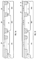
- Fig.'s 2a through 2p illustrate fabrication of the BiCMOS devices shown in Fig. 1.
- Fig. 2a illustrates a cross-section of the devices at a first stage of their fabrication.
- the substrate 10 was masked for simultaneous formation of the n+ well 14 and the npn buried layer 16 with arsenic, antimony, or the like.
- the implant energy used for formation of regions 14 and 16 is preferably between about 50 and 200 KeV, with a preferred range of about 70 to 80 KeV such that the dopant concentration of regions 14 and 16 is between about 1x10¹⁶ and 2x10²⁰, with a preferred range of between about 1x10¹⁹ and 1x10²⁰/cm3.
- the device is then masked for simultaneous formation of the p+ channel stop 19 and the NMOS well 12.
- the implant used in formation of the regions 19 and 12 is preferably between about 10 and 200 KeV with a preferred range of 50 to 150 KeV such that the dopant concentration of the p+ buried layers is between about 1x10¹⁶ and 1x10¹⁸/cm 3.
- the p+ regions preferably are doped with boron.
- the buried layer/channel stop mask is then removed and an intrinsic n-type epitaxial layer having a thickness of about 1.1»m is grown across the surface of the device.
- a photoresist mask is then formed over the device so as to define field oxide regions 22a, 22b, 22c, and 22d.
- the oxide regions are formed using a modified Sidewall Masked Isolation ("SWAMI") process.
- SWAMI Sidewall Masked Isolation
- the substrate is then oxidized in a highly pressurized oxidation environment to grow the necessary field oxide.
- a grown screen oxide layer having a thickness of about 25nm (250 ⁇ ) is formed on the surface of the device and a mask is formed, exposing only the sink region 17.
- a sink implant using an implant energy of between about 100 and 190 KeV with a dose of between about 1x10¹⁴ and 1x10¹⁶ is preferred using phosphorus as a dopant.
- the resulting dopant concentration in the sink region 17 is between about 1x10¹⁹ and 1x10²⁰/cm3.
- the sink mask is then removed and a separate mask/ion implantation is performed to dope the well and channel region of the PMOS transistor to a concentration of between about 1x10¹⁶ and 1x10¹⁷ using phosphorus as a dopant.
- the implant energy used for the PMOS channel region is between about 50 and 180 KeV.
- the resulting net dopant concentration in the channel region is between about and 1x10¹⁶ and 1x10²⁰.
- the sink and n-well are then annealed and driven-in by heating with a conventional thermal cycle in nitrogen.
- a mask is formed on the surface of the device which exposes only the NMOS and PMOS transistor regions.
- This mask is used for a threshold voltage implant as shown in Fig. 2b.
- the implant may be used to adjust the threshold voltage of the NMOS and PMOS transistors as necessary, typically to between about
- the threshold voltage implant is an implant of boron at a dose of between about 1x10¹² to 1x10¹³ and on energy between 30 and 100 KeV, preferably about 50 KeV.
- the threshold voltage implant sets the threshold of the MOS transistors. The boron and the up-diffusing p+ from the buried layer will set the well profile for the NMOS transistor.
- the threshold voltage implant in conjunction with the n-well implant sets the threshold voltage for the PMOS transistor.
- the threshold voltage implant ultimately provides transistors with threshold voltages of about 0.7 to 0.9 volts for NMOS and -0.8 to -1.0 volts for PMOS.
- the screen oxide then is stripped and a thin (on the order of 10 (100) to 20nm (200 ⁇ ), preferably 13,5-16,5nm (135-165 ⁇ )) gate oxide layer 59 is grown using means well known to those of skill in the art.
- a thin (on the order of 10 (100) to 100nm (1000 ⁇ ), preferably 40-60nm (400-600 ⁇ )) layer of polysilicon 60 is then deposited on the thin gate oxide layer and a mask 62 is formed on the poly layer to define the NMOS and PMOS gates.
- a plasma etch removes the undesired polysilicon from all regions of the device except those over the NMOS and PMOS gates to provide the configuration as shown in Fig. 2c.
- a wet etch is used to remove the underlying oxide.
- Fig. 2d illustrates the next sequence of process steps.
- Another layer of intrinsic polysilicon 64 having a thickness of about 100 (1000) to 400nm (4000 ⁇ ), preferably about 320nm (3200 ⁇ ) is deposited across the surface of the device and a cap oxide layer 66 is formed by thermal oxidation of the polysilicon layer 64.
- the devices are then masked with photoresist to expose at least the base region of the bipolar transistor and the lightly doped regions of the resistors. In some embodiments, only the NMOS and PMOS transistor regions are protected by the mask.
- a base implant is then performed and the base is annealed.
- the base implant uses an energy of between about 30 and 100 KeV, with an implant energy of between about 30 and 50 KeV and a dose of about 3x10¹³ to 8x10¹³ preferred.
- An anneal is performed by heating the structure to about 950 °C for about 45 minutes, and results in a p- base region having a thickness of between about 100 (1000) and 200nm (2000 ⁇ ) with a dopant concentration of between about 1x10¹⁸ and 1x10¹⁹/cm3, with a dopant concentration of about 5x10¹⁸/cm3 preferred.
- a mask is formed which exposes regions 68a, 68b, and 68c which will eventually be used as the bipolar emitter contact, the NMOS gate, and the PMOS gate.
- the regions 68a, 68b, 68c are doped n+ using an arsenic implant with an energy of about 100 KeV to a concentration of between about 5x10¹⁹ and 1x10²⁰/cm3.
- the NMOS and PMOS gates may be either n+ or p+ and thus may be implanted using an n+ or a p+ mask.
- the NMOS and PMOS gates will be described as being n+ doped.
- a layer of nitride 69 having a thickness of between about 100 (1000) and 120nm (1200 ⁇ ) is deposited for the purpose of preventing undercutting of the underlying silicon.
- the polysilicon layer 64 is then annealed at 850 to 950 °C for a time of about 10 to 20 minutes.
- a mask is formed on the surface of the nitride to define the collector of the bipolar transistor and the gate of the NMOS and PMOS transistors.
- a dry etch with chlorine chemistry results in the structure shown in Fig. 2g.
- the mask is removed and a photoresist mask is formed to expose the source and drain region of the NMOS transistor.
- a lightly doped drain (LDD) implant is performed in which the source and the drain are lightly implanted with an n-type dopant such as phosphorous or arsenic and using an implant energy of between about 20 and 100 KeV with implant energies of between about 20 and 50 KeV preferred.
- LDD lightly doped drain
- This implant results in a net dopant concentration in the source and drain regions 72 of the NMOS transistor of between about 1x10¹⁷ and 1x10¹⁹.
- a p-type LDD using a dopant such as BF2 or B+ is performed across the surface of the bipolar transistor and the PMOS transistor with only the source and drain of the PMOS transistor and the base region of the bipolar transistor exposed by a mask.
- a more heavily doped p-region 74 is formed in the base of the bipolar transistor and a more heavily doped p-region 76 is formed around the gate of the PMOS transistor, as seen in Fig. 2h.
- the resulting net dopant concentration in the regions 74 and 76 is between about 5x10¹⁷ and 1x10¹⁹/cm3.
- the implant energy is preferably between about between about 10 and 60 KeV. When B+ is used as the dopant, the lower range of implant energy is used.
- LTO Low Temperature Oxide
- a second layer of polysilicon 80 is deposited over the structure.
- the thickness of the layer 80 is preferably no greater than the thickness of the polysilicon layer 64 (Fig. 2d), i.e. , about 400nm (4000 angstroms) or less.
- a planarizing layer 82 is deposited on top of the polysilicon layer 80.
- the planarizing layer 82 can be any of a number of known planarizing materials, including, for example, spin photoresist. As shown in Fig. 2i, the planarizing layer is thinner over the raised emitters and gates and relatively thicker in other regions.
- the polysilicon layer 80 and planarizing layer 82 are dry-etched to produce the configuration depicted in Fig.
- polysilicon in which polysilicon is exposed around the emitter and gates, but remains covered in other areas. A region of polysilicon will also be exposed in the area surrounding the emitters and gates.
- the exposed polysilicon 80 is wet-etched to remove some polysilicon in the exposed region so as to expose the oxide sidewalls, to produce the structure depicted in Fig. 2k.
- the planarizing layers 82 are then removed to produce the structure depicted in Fig. 21. In an alternative embodiment, the planarizing layer 82 is removed from the structure depicted in Fig. 2j prior to the wet-etch of the polysilicon.
- a mask is formed which exposes regions 84a, 84b, 84c, 84d, and 84e (Fig. 2m).
- the regions are then doped p+ to a concentration of between about 1x10¹⁷ and 1x10²⁰, with a dopant concentration of about 1x10¹⁹, preferably using boron.
- the p+ mask is removed and another mask is formed on the surface of the device to expose regions 86a, 86b, and 86c (Fig. 2m).
- the regions 86 are doped n+, using an implant energy of about 100 KeV to a concentration of between about 1x10¹⁸ and 1x10²⁰, with a dopant concentration of between about 1x10¹⁹ and 1x10²⁰/cm3, preferably using arsenic.
- Additional masking and implants can be performed to produce, for example, p-region 88 for forming poly-resistors.
- the described process includes forming the p+ doped regions prior to forming the n+ doped regions, it is equally feasible to form the n+ doped regions prior to the p+ doped regions.
- the polysilicon is annealed by heating to about 850 to 950°C for about 10 to 20 minutes.
- Another mask is then formed over the device for the protection of the desired doped polysilicon regions, and the device is etched with chlorine or bromine chemistry to pattern the polysilicon, producing the configuration depicted in Fig. 2n.
- a layer of screen oxide is formed on the surface of the device over regions where it is desired not to form silicide, such as on the resistors.
- a layer of refractory metals such as titanium, molybdenum, tantalum, tungsten, or the like, is then deposited across the surface of the device.
- the layer is heated to about 750°C for about 10 seconds, preferably using a rapid thermal anneal (RTA), as needed to form an initial amount of silicide that will adhere to the adjacent layers of polysilicon.
- RTA rapid thermal anneal
- the refractory metal does not react with SiO2. Unreacted metal, principally metal in contact with any oxide, is removed, for example, using H2O2 or NH3OH.
- the device is again heated to cause a second silicide reaction to occur, completing the reaction between the refractory metal and adjacent polysilicon and epitaxial silicon.
- the reaction is preferably conducted in two steps, as described, because reaction of a refractory metal in a single step or pulse may cause undesirable reaction of the refractory metal with the sidewall oxide layers.
- the resulting structure is depicted in Fig. 2o.
- the silicide layer 46a extends up to and contacts the sidewall oxide 44 in the bipolar device.
- the silicide layers 54a, 54b, 54c, 54d extend up to and contact the sidewall layers 42, 42′ of the MOS devices.
- an oxide layer 56 is deposited and masked, as is well known in the art, to form contact holes therein.
- Metal 58 is deposited on the surface of the device, masked, and etched from selected regions, providing the device shown in Fig. 1.
Landscapes
- Metal-Oxide And Bipolar Metal-Oxide Semiconductor Integrated Circuits (AREA)
- Bipolar Transistors (AREA)
- Electrodes Of Semiconductors (AREA)
- Internal Circuitry In Semiconductor Integrated Circuit Devices (AREA)
- Weting (AREA)
Claims (3)
- Procédé pour former un dispositif de transistor comprenant successivement les étapes de procédé consistant à :
fournir un substrat en silicium (10);
former au moins une première couche dopée enterrée (14) dans ledit substrat (10);
former une première couche de polysilicium (64) sur la surface dudit substrat;
doper ladite première couche de polysilicium (64);
former une couche de nitrure (69) sur au moins des parties de ladite première couche de polysilicium (64);
retirer les parties sélectionnées de ladite première couche de polysilicium (64) pour configurer ladite couche afin de fournir une première région de polysilicium (68c) sur ledit substrat dans la zone se trouvant au-dessus de ladite première couche enterrée, ladite première région de polysilicium (68c) ayant une surface supérieure et des première et deuxième surfaces de paroi latérale;
recuire ledit substrat (10) en utilisant la première région de polysilicium (68c) comme masque;
implanter des parties dudit substrat pour former des régions de source et de drain (76) pour un dispositif à effet de champ;
déposer de l'oxyde espaceur sur sensiblement la totalité de la surface dudit substrat (10) et de ladite région de polysilicium (68c);
graver à sec ledit oxyde pour éliminer des parties sélectionnées dudit oxyde, laissant des couches (42′) d'oxyde adjacentes auxdites première et deuxième parois latérales desdites premières régions de polysilicium;
déposer une deuxième couche de polysilicium (80) sur sensiblement toute la surface dudit substrat (10) et de ladite première région de polysilicium (68c);
déposer une couche d'aplanissement (82);
graver à sec la surface supérieure de ladite deuxième couche de polysilicium déposée (80) et de ladite couche d'aplanissement (82);
graver par voie humide la surface supérieure de ladite deuxième couche de polysilicium déposée (80) pour fournir ladite deuxième couche de polysilicium (80) s'étendant jusqu'auxdits premier et deuxième espaceurs (42′), ladite deuxième couche de polysilicium (80) étant séparée de ladite première région de polysilicium (68c) seulement par lesdits premier et deuxième espaceurs (42′);
implanter des parties (84d, 84e) de ladite deuxième couche de polysilicium (80) et recuire ledit silicium implanté;
masquer et graver ladite deuxième couche de polysilicium (80) pour éliminer des parties sélectionnées de celle-ci pour fournir une configuration désirée;
former un revêtement, ledit revêtement s'étendant à la fois au-dessus de ladite surface supérieure de ladite première région de polysilicium et d'au moins une partie de la surface supérieure de ladite deuxième couche de polysilicium, ledit revêtement comprenant un métal réfractaire, ladite étape de formation d'un revêtement étant réalisée après ladite étape de masquage et de gravage de ladite deuxième couche de polysilicium et après ladite étape d'implantation des parties (84d, 84e) de ladite deuxième couche de polysilicium (80);
faire réagir ledit métal avec le polysilicium adjacent pour produire une couche de siliciure (52, 54c, 54d) couvrant au moins une partie de ladite partie supérieure de ladite première région de polysilicium (68c) et au moins une partie de ladite deuxième couche de polysilicium (80) et s'étendant jusqu'aux premier et deuxième espaceurs (42′); et
éliminer les parties n'ayant pas réagi dudit métal réfractaire. - Procédé selon la revendication 1 comprenant en outre le dopage de ladite première région de polysilicium (68c) pour configurer ladite première région de polysilicium (68c) comme une grille d'un transistor à effet de champ.
- Procédé selon la revendication 1 dans lequel ledit substrat (10) comprend une couche épitaxiale.
Applications Claiming Priority (2)
| Application Number | Priority Date | Filing Date | Title |
|---|---|---|---|
| US50290290A | 1990-04-02 | 1990-04-02 | |
| US502902 | 1990-04-02 |
Publications (2)
| Publication Number | Publication Date |
|---|---|
| EP0450376A1 EP0450376A1 (fr) | 1991-10-09 |
| EP0450376B1 true EP0450376B1 (fr) | 1995-05-24 |
Family
ID=23999885
Family Applications (1)
| Application Number | Title | Priority Date | Filing Date |
|---|---|---|---|
| EP91104090A Expired - Lifetime EP0450376B1 (fr) | 1990-04-02 | 1991-03-16 | Dispositif BiCMOS ayant des contacts peu espacés et procédé de fabrication |
Country Status (4)
| Country | Link |
|---|---|
| EP (1) | EP0450376B1 (fr) |
| JP (1) | JP3190370B2 (fr) |
| KR (1) | KR100227873B1 (fr) |
| DE (1) | DE69109919T2 (fr) |
Families Citing this family (3)
| Publication number | Priority date | Publication date | Assignee | Title |
|---|---|---|---|---|
| JPH088268A (ja) * | 1994-06-21 | 1996-01-12 | Mitsubishi Electric Corp | バイポーラトランジスタを有する半導体装置およびその製造方法 |
| US6972466B1 (en) * | 2004-02-23 | 2005-12-06 | Altera Corporation | Bipolar transistors with low base resistance for CMOS integrated circuits |
| JP2010278464A (ja) * | 2010-08-06 | 2010-12-09 | Sharp Corp | 半導体装置の製造方法 |
Family Cites Families (2)
| Publication number | Priority date | Publication date | Assignee | Title |
|---|---|---|---|---|
| JPH0628266B2 (ja) * | 1986-07-09 | 1994-04-13 | 株式会社日立製作所 | 半導体装置の製造方法 |
| KR880005690A (ko) * | 1986-10-06 | 1988-06-30 | 넬손 스톤 | 선택적인 에피켁샬층을 사용한 BiCMOS 제조방법 |
-
1991
- 1991-03-16 DE DE69109919T patent/DE69109919T2/de not_active Expired - Fee Related
- 1991-03-16 EP EP91104090A patent/EP0450376B1/fr not_active Expired - Lifetime
- 1991-03-30 KR KR1019910005080A patent/KR100227873B1/ko not_active Expired - Fee Related
- 1991-04-01 JP JP14224891A patent/JP3190370B2/ja not_active Expired - Fee Related
Non-Patent Citations (1)
| Title |
|---|
| IEDM TECHNICAL DIGEST, 1987, pages 24,25 * |
Also Published As
| Publication number | Publication date |
|---|---|
| DE69109919D1 (de) | 1995-06-29 |
| JPH04226063A (ja) | 1992-08-14 |
| KR100227873B1 (ko) | 1999-11-01 |
| JP3190370B2 (ja) | 2001-07-23 |
| DE69109919T2 (de) | 1996-01-04 |
| KR910019217A (ko) | 1991-11-30 |
| EP0450376A1 (fr) | 1991-10-09 |
Similar Documents
| Publication | Publication Date | Title |
|---|---|---|
| US5079182A (en) | Bicmos device having self-aligned well tap and method of fabrication | |
| US5424572A (en) | Spacer formation in a semiconductor structure | |
| EP0283135B1 (fr) | Procédé de fabrication d'une structure semi-conductrice | |
| US4760033A (en) | Method for the manufacture of complementary MOS field effect transistors in VLSI technology | |
| US5338694A (en) | Method of fabricating BiCMOS device | |
| US5169794A (en) | Method of fabrication of pnp structure in a common substrate containing npn or MOS structures | |
| EP0256904B1 (fr) | Méthode pour fabriquer des structures BiCMOS à haute performance ayant des émetteurs en polysilicium et des bases silicidées | |
| US4929570A (en) | Selective epitaxy BiCMOS process | |
| EP0450375B1 (fr) | Interconnexion et procédé de fabrication pour des dispositifs à semi-conducteurs | |
| US5231042A (en) | Formation of silicide contacts using a sidewall oxide process | |
| US5407840A (en) | Method for simultaneously fabricating bipolar and complementary field effect transistors | |
| US5374566A (en) | Method of fabricating a BiCMOS structure | |
| US5234847A (en) | Method of fabricating a BiCMOS device having closely spaced contacts | |
| WO1995001653A1 (fr) | Transistors et leur procede de fabrication | |
| EP0451553B1 (fr) | Transistor bipolaire avec base silicideure auto-alignée et résistance et méthode de fabrication | |
| US5443994A (en) | Method of fabricating a semiconductor device having a borosilicate glass spacer | |
| US5298440A (en) | Method of fabrication of transistor device with increased breakdown voltage | |
| US5124775A (en) | Semiconductor device with oxide sidewall | |
| EP0263756B1 (fr) | Procédé BiCMOS utilisant une épitaxie sélective | |
| EP0450376A1 (fr) | Dispositif BiCMOS ayant des contacts peu espacés et procédé de fabrication |
Legal Events
| Date | Code | Title | Description |
|---|---|---|---|
| PUAI | Public reference made under article 153(3) epc to a published international application that has entered the european phase |
Free format text: ORIGINAL CODE: 0009012 |
|
| AK | Designated contracting states |
Kind code of ref document: A1 Designated state(s): DE FR GB IT |
|
| 17P | Request for examination filed |
Effective date: 19920215 |
|
| 17Q | First examination report despatched |
Effective date: 19930526 |
|
| GRAA | (expected) grant |
Free format text: ORIGINAL CODE: 0009210 |
|
| AK | Designated contracting states |
Kind code of ref document: B1 Designated state(s): DE FR GB IT |
|
| PG25 | Lapsed in a contracting state [announced via postgrant information from national office to epo] |
Ref country code: IT Free format text: LAPSE BECAUSE OF FAILURE TO SUBMIT A TRANSLATION OF THE DESCRIPTION OR TO PAY THE FEE WITHIN THE PRE;WARNING: LAPSES OF ITALIAN PATENTS WITH EFFECTIVE DATE BEFORE 2007 MAY HAVE OCCURRED AT ANY TIME BEFORE 2007. THE CORRECT EFFECTIVE DATE MAY BE DIFFERENT FROM THE ONE RECORDED.SCRIBED TIME-LIMIT Effective date: 19950524 Ref country code: FR Effective date: 19950524 |
|
| REF | Corresponds to: |
Ref document number: 69109919 Country of ref document: DE Date of ref document: 19950629 |
|
| EN | Fr: translation not filed | ||
| PG25 | Lapsed in a contracting state [announced via postgrant information from national office to epo] |
Ref country code: GB Effective date: 19960316 |
|
| PLBE | No opposition filed within time limit |
Free format text: ORIGINAL CODE: 0009261 |
|
| STAA | Information on the status of an ep patent application or granted ep patent |
Free format text: STATUS: NO OPPOSITION FILED WITHIN TIME LIMIT |
|
| 26N | No opposition filed | ||
| GBPC | Gb: european patent ceased through non-payment of renewal fee |
Effective date: 19960316 |
|
| PGFP | Annual fee paid to national office [announced via postgrant information from national office to epo] |
Ref country code: DE Payment date: 20090327 Year of fee payment: 19 |
|
| PG25 | Lapsed in a contracting state [announced via postgrant information from national office to epo] |
Ref country code: DE Free format text: LAPSE BECAUSE OF NON-PAYMENT OF DUE FEES Effective date: 20101001 |