EP0256904B1 - Méthode pour fabriquer des structures BiCMOS à haute performance ayant des émetteurs en polysilicium et des bases silicidées - Google Patents
Méthode pour fabriquer des structures BiCMOS à haute performance ayant des émetteurs en polysilicium et des bases silicidées Download PDFInfo
- Publication number
- EP0256904B1 EP0256904B1 EP87401630A EP87401630A EP0256904B1 EP 0256904 B1 EP0256904 B1 EP 0256904B1 EP 87401630 A EP87401630 A EP 87401630A EP 87401630 A EP87401630 A EP 87401630A EP 0256904 B1 EP0256904 B1 EP 0256904B1
- Authority
- EP
- European Patent Office
- Prior art keywords
- layer
- region
- conductivity type
- regions
- forming
- Prior art date
- Legal status (The legal status is an assumption and is not a legal conclusion. Google has not performed a legal analysis and makes no representation as to the accuracy of the status listed.)
- Expired
Links
Images

Classifications
-
- H—ELECTRICITY
- H10—SEMICONDUCTOR DEVICES; ELECTRIC SOLID-STATE DEVICES NOT OTHERWISE PROVIDED FOR
- H10D—INORGANIC ELECTRIC SEMICONDUCTOR DEVICES
- H10D84/00—Integrated devices formed in or on semiconductor substrates that comprise only semiconducting layers, e.g. on Si wafers or on GaAs-on-Si wafers
- H10D84/40—Integrated devices formed in or on semiconductor substrates that comprise only semiconducting layers, e.g. on Si wafers or on GaAs-on-Si wafers characterised by the integration of at least one component covered by groups H10D12/00 or H10D30/00 with at least one component covered by groups H10D10/00 or H10D18/00, e.g. integration of IGFETs with BJTs
- H10D84/401—Combinations of FETs or IGBTs with BJTs
-
- H—ELECTRICITY
- H10—SEMICONDUCTOR DEVICES; ELECTRIC SOLID-STATE DEVICES NOT OTHERWISE PROVIDED FOR
- H10D—INORGANIC ELECTRIC SEMICONDUCTOR DEVICES
- H10D84/00—Integrated devices formed in or on semiconductor substrates that comprise only semiconducting layers, e.g. on Si wafers or on GaAs-on-Si wafers
- H10D84/01—Manufacture or treatment
- H10D84/0107—Integrating at least one component covered by H10D12/00 or H10D30/00 with at least one component covered by H10D8/00, H10D10/00 or H10D18/00, e.g. integrating IGFETs with BJTs
- H10D84/0109—Integrating at least one component covered by H10D12/00 or H10D30/00 with at least one component covered by H10D8/00, H10D10/00 or H10D18/00, e.g. integrating IGFETs with BJTs the at least one component covered by H10D12/00 or H10D30/00 being a MOS device
-
- H—ELECTRICITY
- H10—SEMICONDUCTOR DEVICES; ELECTRIC SOLID-STATE DEVICES NOT OTHERWISE PROVIDED FOR
- H10D—INORGANIC ELECTRIC SEMICONDUCTOR DEVICES
- H10D84/00—Integrated devices formed in or on semiconductor substrates that comprise only semiconducting layers, e.g. on Si wafers or on GaAs-on-Si wafers
- H10D84/01—Manufacture or treatment
- H10D84/02—Manufacture or treatment characterised by using material-based technologies
- H10D84/03—Manufacture or treatment characterised by using material-based technologies using Group IV technology, e.g. silicon technology or silicon-carbide [SiC] technology
- H10D84/038—Manufacture or treatment characterised by using material-based technologies using Group IV technology, e.g. silicon technology or silicon-carbide [SiC] technology using silicon technology, e.g. SiGe
-
- H—ELECTRICITY
- H10—SEMICONDUCTOR DEVICES; ELECTRIC SOLID-STATE DEVICES NOT OTHERWISE PROVIDED FOR
- H10W—GENERIC PACKAGES, INTERCONNECTIONS, CONNECTORS OR OTHER CONSTRUCTIONAL DETAILS OF DEVICES COVERED BY CLASS H10
- H10W15/00—Highly-doped buried regions of integrated devices
-
- H—ELECTRICITY
- H10—SEMICONDUCTOR DEVICES; ELECTRIC SOLID-STATE DEVICES NOT OTHERWISE PROVIDED FOR
- H10W—GENERIC PACKAGES, INTERCONNECTIONS, CONNECTORS OR OTHER CONSTRUCTIONAL DETAILS OF DEVICES COVERED BY CLASS H10
- H10W15/00—Highly-doped buried regions of integrated devices
- H10W15/01—Manufacture or treatment
-
- Y—GENERAL TAGGING OF NEW TECHNOLOGICAL DEVELOPMENTS; GENERAL TAGGING OF CROSS-SECTIONAL TECHNOLOGIES SPANNING OVER SEVERAL SECTIONS OF THE IPC; TECHNICAL SUBJECTS COVERED BY FORMER USPC CROSS-REFERENCE ART COLLECTIONS [XRACs] AND DIGESTS
- Y10—TECHNICAL SUBJECTS COVERED BY FORMER USPC
- Y10S—TECHNICAL SUBJECTS COVERED BY FORMER USPC CROSS-REFERENCE ART COLLECTIONS [XRACs] AND DIGESTS
- Y10S257/00—Active solid-state devices, e.g. transistors, solid-state diodes
- Y10S257/90—MOSFET type gate sidewall insulating spacer
Definitions
- This invention relates to processes for manufacturing integrated circuits, and to a process for simultaneously fabricating bipolar and complementary field effect transistors in a semiconductor substrate. More particularly, the invention relates to the fabrication of such devices having lower base resistance and a polysilicon emitter, and to the fabrication of a completed BiCMOS structure having very high performance.
- CMOS complementary metal oxide semiconductor
- Bipolar and complementary metal oxide semiconductor (CMOS) technologies have each been independently understood for many years.
- BiCMOS bipolar output drivers may be employed with CMOS memories to provide more drive current.
- MOS slows down as temperature rises while bipolar speeds up
- a CMOS bipolar combination may be employed to make devices less speed sensitive to temperature.
- Combining high performance bipolar devices with MOS transistors on the same integrated circuit allows a combination of the high-packing density of MOS devices with the high speed of bipolar and permits the integration of complex functions with high yields.
- the CMOS transistors with their inherently low power requirements have large noise margins, while the bipolar devices have an advantage in switching speed and greater current drive per unit area.
- US-A-4,484,388 discloses a method for forming a Bi-CMOS structure including a vertical npn-transistor and CMOS transistors on a common semiconductor substrate.
- a p-type epitaxial layer is formed on a p-type silicon substrate with a plurality of n+-type buried layers therein.
- N-type wells are formed to extend to the n+-type buried layers.
- Field oxide films are formed to define an n-type element region for the npn-transistor, an n-type element region for the PMOS-transistor, and a p-type element region for the NMOS-transistor.
- a gate oxide layer for the CMOS is formed on the surfaces of all element regions.
- a p-type active base region for the npn-transistor is formed by boron ion implantation, and an emitter electrode comprising an arsenic-doped polysilicon layer contacts the base region.
- CMOS gate electrodes exhibit low resistance due to phosphorus and/or arsenic doping.
- the emitter electrode is utilized as a diffusion source to form an n-type emitter region. Boron ion implantation results simultaneously in a p+ -type external base region and p+-type source and drain regions of the PMOS-transistor while phosphorus ion implantation results in an n+-type collector contact region and n+-type source and drain regions of the NMOS-transistor. With few masking steps, the device performance does not satisfy, and the document teaches multiple masking steps in order to achieve improved performance.
- FR-A-2 134 360 discloses a method for fabricating monolithic semiconductor devices including the following steps: Provision of a semiconductor substrate of a first conductivity type, introduction thereinto of two impurities of opposite conductivity and of different diffusion rate at predetermined zones, forming of an epitaxial layer of the first conductivity type on the substrate, treatment of the substrate including the epitaxial layer so as to cause complete rediffusion of one of the impurities through all of the epitaxial layer to reach its surface opposite the interface with the substrate, and forming at a predefined site of the surface a bipolar transistor. At other sites of the device, field effect transistors may be formed.
- the two impurities may be arsenic and phosphorus, respectively.
- the base of the bipolar transistor may be formed in a single diffusion step simultaneously with source and drain of a first field effect transistor, and the emitter of the bipolar transistor may be formed in a single diffusion step simultaneously with source and drain of the second field effect transistor.
- CMOS complementary metal-oxide-semiconductor
- our method of fabricating a BiCMOS semiconductor structure on a first conductivity substrate begins with the formation of an opposite conductivity buried layer by the steps of introducing into at least one first region of the substrate a first impurity of N conductivity type, typically arsenic, and then introducing into the first region a second impurity of N conductivity type, typically phosphorus. Then, a blanket implantation of the substrate with P conductivity type impurity which will form the P buried layers beneath the P wells of the structure is performed. The P wells are used for fabrication of NMOS devices. An epitaxial layer is formed over the substrate, and parts of the epitaxial layer overlying the buried layers are doped with N conductivity type impurity.
- the structure is then heated to cause the N conductivity type impurity regions in the epitaxial layer and in the substrate to diffuse to contact each other.
- this process results in the fabrication of buried layers which have low resistance, yet high diffusivity to lower the capacitance between the substrate and the buried layers.
- the process assures that the preferably N type buried layers join with the N conductivity type well formed in the epitaxial layer for the P channel MOS devices and NPN bipolar devices. Accurate control of the N well dopant and fabrication of the buried layers in a shorter time minimize the effects of prolonged high-temperature processing.
- the method then includes the steps of forming an insulating layer over the surface of the silicon layer, and forming a conductive protective layer, typically polycrystalline silicon, over all of the insulating material.
- the insulating layer then is removed from the surface of the epitaxial silicon layer in the bipolar region and first conductivity type impurity is introduced into a part of the bipolar area to define the base. Additional conductive material is deposited over at least the bipolar region, and all of the protective layer is removed from the insulating layer except where gates and the emitter are desired. The sources and drains then are doped.
- the initially formed insulating layer will provide the gate oxide, while the protective layer provides the polycrystalline silicon electrodes for the MOS devices.
- the single mask defines both the base of the bipolar devices and distinguishes the bipolar devices from the CMOS devices. Later in the process a single mask defines both the gates and the emitter for the structure.
- the protective layer not only serves as the gate electrodes, but also protects the gate oxide from the effect of subsequent processing to prevent the etching of openings in the gate oxide in places other than desired.
- the semiconductor structure from our process has a lower base resistance for the bipolar devices and is fabricated in a smaller area. The reduced area lowers the capacitance and increases the speed of the circuit. Forming the additional protective material adjacent the field oxide creates a walled emitter structure, while providing less sensitivity to alignment tolerances.
- front-end and back-end processes are used to form the semiconductor structure through the buried layers and epitaxial layer, while the back-end processes are used to complete the structure.
- back-end processes are used to complete the structure.
- a single front-end process may be combined with any one of a variety of back-end processes while a single back-end process may be combined with any one of a variety of front-end processes.
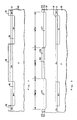
- Figure 1 is a cross-sectional view of a semiconductor substrate 10 having a crystalline orientation of ⁇ 100>, and which has been doped with P conductivity type impurity to a resistivity of 11-18 ohm centimeters.
- the silicon substrate may be protected with a thin layer of silicon dioxide and alignment marks formed therein. This step may be eliminated if the later-formed buried layer regions are to be used for alignment.
- Mask 15 typically will comprise photoresist, applied and defined using well known photolithographic or other techniques. Openings are made in mask 15 wherever an N conductivity type buried layer is desired. N type buried layers are desired wherever the P channel MOS devices and NPN bipolar devices will be formed. No N type buried layer is fabricated where N channel MOS devices are desired.
- a first N conductivity type impurity is implanted, followed in the preferred embodiment by a second N conductivity type impurity implanted in the same region.
- the N type impurity dopants are shown as regions 18 in Figure 1.
- the first N type impurity is phosphorus introduced with a dosage of 3x10¹³ to 3x10¹⁴ atoms per square centimeter, while the second impurity is arsenic at a dosage of 1x10¹⁵ to 1x10¹⁶ atoms per square centimeter.
- the arsenic lowers the resistance of the buried layer, the higher diffusivity of phosphorus allows it to diffuse further into the substrate (as well as into an overlying epitaxial layer), to lower the capacitance between the substrate and the buried layer in the bipolar devices.
- the double implant also assures that the N well implant in the epitaxial layer and in the buried layer join during subsequent thermal processing. This advantage is discussed further below.
- a blanket implant of P conductivity type impurity 12 is introduced across the entire surface of the substrate. This impurity ultimately will form a P conductivity type buried layer for the N channel CMOS transistors.
- an upper portion 12 of substrate 10 is doped with 3x10¹² to 5x10¹³ atoms per square centimeter of boron.
- epitaxial layer 21 is deposited across the silicon substrate 10 in the manner shown in Figure 2.
- epitaxial layer 21 is undoped, and about 1 to 2 ⁇ m (microns) thick.
- the formation of such epitaxial layers is well known.
- a thin layer of protective silicon dioxide (not shown) is formed by oxidizing the upper surface of the epitaxial layer.
- an N well mask 24 is formed across the upper surface of the epitaxial layer (or silicon dioxide) to define the regions where N conductivity type wells are desired in the epitaxial layer. As shown in Figure 2, such wells are desired for electrical isolation of the PMOS and NPN devices.
- the N well mask comprises photoresist, which may be patterned using the same mask as the N type buried layers. Alternatively, and as shown in Figure 3 by the relative dimensions of the N-wells and buried layers, an oversize mask may be used.
- the N conductivity type wells are implanted, preferably using phosphorus and a dose of 1-2x10¹² atoms per square centimeter.
- the surface of the epitaxial layer 21 is again cleaned and reoxidized by heating it to a temperature of 900°C for 30-60 minutes to form about 25-50 nm (250-500 Angstroms) of silicon dioxide 33 across the entire epitaxial layer 21.
- a layer of silicon nitride 35 approximately 120-170 nm (1200-1700 Angstroms) thick is deposited, preferably using chemical vapor deposition, across the surface of silicon dioxide 33.
- silicon nitride layer 35 is removed from the surface of the silicon dioxide 33 wherever regions of field oxide 39 are desired.
- the field oxide is formed at the intersections of the N wells 27 and 28 with the P well 30.
- regions of silicon dioxide are annular when viewed from above and serve to separate the N and P wells from each other at the surface.
- Additional regions of field oxide 39 are formed within the N and P wells themselves, for example, as shown in N well 28 for the NPN transistor, to allow a connection to the buried collector, which connection is isolated from the extrinsic base.
- the field oxide allows an isolated tap to the substrate, as it does in the P well 30.
- a field implant may be performed if desired. Such an implant assists in preventing channel inversion at the silicon dioxide-silicon interface resulting from impurity in the silicon dioxide field regions.
- the field implant employs boron and a dose of 5x10¹² to 2x10¹³ atoms per square centimeter. Unlike prior art processes, no mask is required for this implant. Our process uses the nitride layer 35 as the mask and later process steps compensate for the P type dopant beneath the field regions.
- the structure is raised to a temperature of about 1050-1100°C for 1-2 hours in Nitrogen to diffuse the P and N conductivity type impurities employed to form the buried layers and wells. Then, the field is oxidized to create silicon dioxide regions 39. In the preferred embodiment such regions are approximately 600 nm (6000 Angstroms) thick formed by heating the structure to about 900°C for 400 minutes. The appearance of the structure following this process is shown in Figure 3. Note that the phosphorus has diffused up from the buried layer to contact the downwardly diffusing N well.
- the BiCMOS process of our invention as thus far performed provides several unique advantages over prior art processes.
- the arsenic lowers the resistance of the buried layer 18, while the phosphorus lowers substrate/buried layer capacitance and assures that the N well implant 27 and buried layer 18 join during a relatively short thermal process.
- our process minimizes the exposure of the structure to prolonged high temperatures and the resulting degradation, while speeding manufacture of the circuit.
- an undoped silicon epitaxial layer we allow accurate control of the P well dopant.
- the process allows minimizing the resistance of both the P and N wells, yet maintaining the doping concentrations thereof at a sufficiently low amount to minimize capacitance between the wells. High levels will lower performance of the bipolar devices and lower breakdown voltages for the CMOS devices.
- Our process prevents diffusion between the N and P wells to permit a closer spacing of those wells for denser CMOS structures.
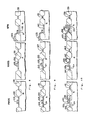
- the thin silicon dioxide layer 33 and silicon nitride layer 35 are removed from the surface of the structure.
- a layer of gate oxide 100 is formed by heating the substrate in an oxidizing ambient to a temperature of 900°C for approximately 2-4 minutes.
- a relatively thin layer of protective material typically polycrystalline silicon 30-100 nm (300-1000 Angstroms) in thickness, is deposited across the entire surface of the structure.
- Polycrystalline silicon layer 103 is formed using a well known chemical vapor deposition processes. This first layer of polycrystalline silicon protects the gate oxide for the fabrication of subsequent MOS devices and prevents the etching of openings in the gate oxide in places other than where the gate oxide is to be removed.
- a photoresist mask 108 is defined across the surface of the structure, and using well known techniques, an oversized opening is created where the base of the NPN transistor is to be formed.
- the exposed polysilicon 103 is etched away using well known techniques, and the bipolar base is implanted with boron, typically with a dose of on the order of 1x10¹³ to 1x10¹⁴ atoms per square centimeter at 40-100 KeV.
- base region 110 is formed beneath the thin oxide 100 in the manner depicted in Figure 6.
- the gate oxide is removed from the surface of the NPN transistor area.
- a layer of conductive material 103 also polycrystalline silicon, is deposited across the entire surface of the structure.
- layer 103 will be thinner than on other regions of the structure. Because the gate oxide was removed from the surface of the NPN device area, the polycrystalline silicon is deposited directly on the silicon in that region.
- Polysilicon layer 103 is then implanted with arsenic to lower its resistance. In the preferred embodiment, a dose of 1x10¹⁵ to 1x10¹⁶ atoms per square centimeter is used.
- a new mask 114 is formed to protect regions where gates of the CMOS devices and a walled emitter of the bipolar device are desired.
- a single mask defines both the gates and the emitter.
- the exposed portions of polysilicon layer 103 are removed using well known chemical or plasma processes.
- the resulting structure is shown in Figure 8.
- the silicon dioxide acts as an etch stop and prevents further etching.
- the absence of the gate oxide layer allows the etchant to attack the underlying silicon and results in a slight overetching of the epitaxial silicon, typically about 300-1000 Angstroms. This overetching results from the need to assure complete removal of the undesired polysilicon 103 from the CMOS device areas and the necessity therefore to extend the etching operation.
- a layer of silicon dioxide (not shown) about 1000-3000 Angstroms thick then is formed across the upper surface of the exposed polysilicon by chemical vapor deposition or other known techniques. Using well known anisotropic etching processes, most of the silicon dioxide is etched from the surface of the structure to leave only oxidized sidewall spacer regions such as base contact spacer 132 and source/drain contact spacer regions 135. In the preferred embodiment such spacer regions will be about 1000-3000 Angstroms wide.
- N conductivity type impurity is implanted through the mask openings.
- a first dose of phosphorus of 1x10¹³ to 1x10¹⁴ atoms per square centimeter followed by a second dose of arsenic of 6x10¹⁵ atoms per square centimeter at 100 KeV are employed.
- Two impurities are used to form a lightly doped drain type structure because the phosphorus will diffuse under the spacer oxide 135 toward the channel.
- the implant forms a collector contact 115 for the bipolar transistor, a substrate tap 118 for the P channel MOS device, and source/drain regions 120 for the N channel MOS device.
- a first light dose of N type impurity is introduced before formation of the spacer regions and a second dose of N type impurity is introduced after formation of the spacer regions.
- a P type impurity implant preferably boron at a dose of 3x10¹⁵ atoms per square centimeter and an energy of 50 KeV, is employed to form the P type source and drain 124 of the P channel device and the substrate tap 127 of the N channel device.
- the NPN base and P channel source and drain are separately implanted, their performance may be independently optimized.
- the P and N conductivity type implants are annealed by heating the structure to a temperature of 900°C for 30-90 minutes. During annealing the impurity in the polysilicon contact 103 to the bipolar transistor will diffuse into the epitaxial silicon to form the emitter 130.
- an extrinsic base region implant to lower the base resistance may be performed at this stage of the process by masking all of the structure except for the base region and then introducing additional impurity. If this step is performed, a dose of 5x10¹⁴ to 2x10¹⁵ atoms per square centimeter of boron is employed. The spacer 132 prevents the implant from being placed too close to the emitter.
- silicide forming metal is deposited across the upper surface of the structure and the structure heated to cause the metal to react with the underlying silicon, both polycrystalline and monocrystalline, to form regions of metal silicide. Unreacted metal then is removed selectively by a wet chemical etch. Any metal which will react with silicon to form a silicide may be employed; however, in the preferred embodiment, approximately 50-100 nm (500-1000 Angstroms) of platinum are sputtered onto the surface and the structure heated to 400-450°C for 5-30 minutes to form platinum silicide. Platinum silicide forms excellent contacts to P type regions.
- Silicide region 136 is an electrical contact via polycrystalline silicon 103 to emitter 130 (as well as to any other component such as a nearby resistor formed on field oxide 39), while silicide region 137 is a contact to base region 110.
- the collector contact is silicide contact 138.
- silicide regions 139 provide source/drain contacts, while silicide 140 contacts the gate, and silicide 141 is a substrate tap.
- silicide 142 contacts the source/drain regions, while silicide 143 contacts the gate, and silicide 144 connects to the substrate tap.
- the appearance of the structure after formation of the silicide is depicted in Figure 10.
- the structure may be completed by fabrication of metal connections using conventional techniques.
- the process of our invention provides many advantages over prior art processes. Using a single mask to distinguish the bipolar devices from the CMOS devices, that is, the base mask, and only a single mask to define both the gates and the emitter, high performance devices may be fabricated. Furthermore, the first layer of polycrystalline silicon protects the gate oxide for subsequent MOS devices.
Landscapes
- Metal-Oxide And Bipolar Metal-Oxide Semiconductor Integrated Circuits (AREA)
- Bipolar Transistors (AREA)
Claims (15)
- Procédé de fabrication d'une structure semiconductrice dans une couche de silicium ayant une surface supérieure et ayant une première région (30) d'un premier type de conductivité ainsi qu'une deuxième et une troisième régions (27, 28) d'un deuxième type de conductivité, la première, la deuxième et la troisième régions étant séparées les unes des autres à la surface par des régions de champ (39) d'une couche de matériau isolant insérée dans la couche, le procédé comprenant les étapes consistant à :
former une couche isolante (100) sur la surface de la couche de silicium;
former une couche de protection (103) en un matériau conducteur sur la totalité de la couche isolante à l'exception d'une première partie de la troisième région;
introduire une impureté (110) d'un premier type de conductivité dans la première partie de la troisième région;
utiliser la couche de protection comme un masque, retirer la couche isolante de la surface de la couche du silicium dans la première partie de la troisième région;
déposer un matériau conducteur supplémentaire sur au moins la première partie de la troisième région;
retirer la couche de protection (103) de la couche isolante à l'exception d'une première partie de la première région, une première partie de la deuxième région et une seconde partie de la troisième région, la première partie de chacune des première et deuxième régions étant espacées des régions de champ, au moins une partie de la seconde partie de la troisième région recouvrant la première partie de la troisième région; et à
introduire une impureté (124) d'un premier type de conductivité dans la deuxième région à l'exception de l'endroit recouvert par la couche de protection, et une impureté (120) d'un second type de conductivité dans la première région à l'exception de l'endroit recouvert par la couche de protection. - Procédé selon la revendication 1, comprenant, en outre, après l'étape de dépôt du matériau conducteur supplémentaire, l'étape consistant à doper au moins un matériau conducteur supplémentaire pour diminuer sa résistance.
- Procédé selon la revendication 2, comprenant, en outre, après l'étape de retrait de la couche de protection (103) l'étape consistant à chauffer la structure pour faire diffuser une partie des impuretés du matériau conducteur dans la troisième région.
- Procédé selon la revendication 1, dans lequel l'étape consistant à former une couche isolante (100) comprend l'oxydation de la couche de silicium.
- Procédé selon la revendication 1, dans lequel l'étape consistant à former une couche de protection (103) comprend la formation d'une couche de silicium polycristallin.
- Procédé selon la revendication 5, dans lequel l'étape consistant à déposer le matériau conducteur supplémentaire comprend le dépôt de silicium polycristallin supplémentaire.
- Procédé selon la revendication 5, dans lequel l'étape consistant à former une couche de protection (103) comprend le dépôt d'une couche de protection sur la totalité de la structure et ensuite le retrait de la couche de protection de la première partie de la troisième région.
- Procédé selon la revendication 1, dans lequel l'opération consistant à former une couche isolante (100) fournit une couche d'un matériau isolant pour séparer au moins une électrode de porte d'un transistor à effet de champ du substrat sousjacent.
- Procédé selon la revendication 1, dans lequel lesdites régions de champ insérées (39) comprennent du dioxyde de silicium,- dans lequel ladite couche isolante (100) sur la surface de la couche de silicium comprend du dioxyde de silicium formant une couche de porte isolante,- dans lequel ladite couche de protection (103) de matériau conducteur est une couche de silicium polycristallin,- dans lequel ladite première partie de la troisième région définit une base d'un transistor bipolaire, ladite base étant formée par ladite étape consistant à introduire ladite impureté (110) du premier type de conductivité dans la première partie de la troisième région,- dans lequel ledit matériau conducteur supplémentaire est du silicium polycristallin et est déposé également sur ladite couche de silicium polycristallin,- dans lequel ladite première partie de la première région définit une électrode de porte, ladite première partie de la deuxième région définit une autre électrode de porte, ladite seconde partie de la troisième région définit un contact d'émetteur, et- dans lequel l'étape consistant à introduire l'impureté (124) d'un premier type de conductivité dans la deuxième région définit une source et un drain, et ladite étape consistant à introduire une impureté (120) d'un second type de conductivité dans la première région définit une autre source et un autre drain.
- Procédé selon la revendication 1, dans lequel la couche de silicium ayant une surface supérieure et ayant une première région (30) d'un premier type de conductivité et une deuxième et une troisième région (27, 28) d'un second type de conductivité, la première, la deuxième et la troisième régions étant séparées les unes des autres à la surface par des régions de champ (39) en matériau isolant insérées dans la couche, est formée parun procédé comprenant les étapes consistant à :
introduire une première impureté d'un second type de conductivité dans au moins une première zone d'un substrat;
introduire une seconde impureté d'un second type de conductivité dans la première zone (21);
former une couche épitaxiale sur le substrat produisant ainsi ladite couche de silicium;
introduire une impureté d'un second type de conductivité dans au moins une première partie de la couche épitaxiale recouvrant la première zone du substrat ; et à
chauffer la structure pour entraîner la diffusion de l'impureté du second type de conductivité dans la couche épitaxiale et dans le substrat pour qu'il vienne en contact l'un avec l'autre - Procédé selon la revendication 10, dans lequel l'étape consistant à introduire l'impureté du second type de conductivité dans au moins une première partie de la couche épitaxiale (21) comprend l'introduction de l'impureté du second type de conductivité dans une paire de régions la couche épitaxiale éloignées l'une de l'autre pour définir un premier et un second puits (27, 28), la paire de premières régions espacées l'une de l'autre étant séparée par une région intermédiaire de la couche épitaxiale de type de conductivité opposée pour définir un troisième puits (30).
- Procédé selon la revendication 11, suivit par l'étape consistant à former une couche (33) de matériau isolant sur toute la couche épitaxiale.
- Procédé selon la revendication 12, dans lequel ladite troisième région coïncide avec ledit premier puits (28).
- Procédé selon la revendication 13, dans lequel l'introduction de l'impureté de premier type de conductivité dans le premier puits se produit à travers la première partie.
- Procédé selon l'une des revendications 11 à 14 comprenant l'étape consistant à former des connexions électriques avec chacun des puits.
Applications Claiming Priority (2)
| Application Number | Priority Date | Filing Date | Title |
|---|---|---|---|
| US06/887,007 US4727046A (en) | 1986-07-16 | 1986-07-16 | Method of fabricating high performance BiCMOS structures having poly emitters and silicided bases |
| US887007 | 1986-07-16 |
Publications (2)
| Publication Number | Publication Date |
|---|---|
| EP0256904A1 EP0256904A1 (fr) | 1988-02-24 |
| EP0256904B1 true EP0256904B1 (fr) | 1992-01-29 |
Family
ID=25390260
Family Applications (1)
| Application Number | Title | Priority Date | Filing Date |
|---|---|---|---|
| EP87401630A Expired EP0256904B1 (fr) | 1986-07-16 | 1987-07-10 | Méthode pour fabriquer des structures BiCMOS à haute performance ayant des émetteurs en polysilicium et des bases silicidées |
Country Status (4)
| Country | Link |
|---|---|
| US (1) | US4727046A (fr) |
| EP (1) | EP0256904B1 (fr) |
| JP (1) | JPS6379368A (fr) |
| DE (1) | DE3776460D1 (fr) |
Families Citing this family (34)
| Publication number | Priority date | Publication date | Assignee | Title |
|---|---|---|---|---|
| US4808548A (en) * | 1985-09-18 | 1989-02-28 | Advanced Micro Devices, Inc. | Method of making bipolar and MOS devices on same integrated circuit substrate |
| US4902640A (en) * | 1987-04-17 | 1990-02-20 | Tektronix, Inc. | High speed double polycide bipolar/CMOS integrated circuit process |
| KR0120196B1 (ko) * | 1987-05-13 | 1997-10-17 | 미다 가쓰시게 | 반도체 집적회로장치 및 그 제조방법 |
| US4931407A (en) * | 1987-06-25 | 1990-06-05 | Kabushiki Kaisha Toshiba | Method for manufacturing integrated bipolar and MOS transistors |
| KR900001062B1 (ko) * | 1987-09-15 | 1990-02-26 | 강진구 | 반도체 바이 씨 모오스 장치의 제조방법 |
| US5124817A (en) * | 1988-01-19 | 1992-06-23 | National Semiconductor Corporation | Polysilicon emitter and a polysilicon gate using the same etch of polysilicon on a thin gate oxide |
| US5179031A (en) * | 1988-01-19 | 1993-01-12 | National Semiconductor Corporation | Method of manufacturing a polysilicon emitter and a polysilicon gate using the same etch of polysilicon on a thin gate oxide |
| US5001081A (en) * | 1988-01-19 | 1991-03-19 | National Semiconductor Corp. | Method of manufacturing a polysilicon emitter and a polysilicon gate using the same etch of polysilicon on a thin gate oxide |
| US4912053A (en) * | 1988-02-01 | 1990-03-27 | Harris Corporation | Ion implanted JFET with self-aligned source and drain |
| KR910009739B1 (ko) * | 1988-07-13 | 1991-11-29 | 삼성전자 주식회사 | 반도체장치의 제조방법 |
| US5105253A (en) * | 1988-12-28 | 1992-04-14 | Synergy Semiconductor Corporation | Structure for a substrate tap in a bipolar structure |
| US5256582A (en) * | 1989-02-10 | 1993-10-26 | Texas Instruments Incorporated | Method of forming complementary bipolar and MOS transistor having power and logic structures on the same integrated circuit substrate |
| US5060194A (en) * | 1989-03-31 | 1991-10-22 | Kabushiki Kaisha Toshiba | Semiconductor memory device having a bicmos memory cell |
| JPH0348459A (ja) * | 1989-04-26 | 1991-03-01 | Matsushita Electric Ind Co Ltd | 半導体装置及びその製造方法 |
| US4902639A (en) * | 1989-08-03 | 1990-02-20 | Motorola, Inc. | Process for making BiCMOS integrated circuit having a shallow trench bipolar transistor with vertical base contacts |
| US5112761A (en) * | 1990-01-10 | 1992-05-12 | Microunity Systems Engineering | Bicmos process utilizing planarization technique |
| JP2501930B2 (ja) * | 1990-02-26 | 1996-05-29 | 株式会社東芝 | 半導体集積回路 |
| GB2245418A (en) * | 1990-06-20 | 1992-01-02 | Koninkl Philips Electronics Nv | A semiconductor device and a method of manufacturing such a device |
| US5082796A (en) * | 1990-07-24 | 1992-01-21 | National Semiconductor Corporation | Use of polysilicon layer for local interconnect in a CMOS or BiCMOS technology incorporating sidewall spacers |
| US5238872A (en) * | 1990-12-11 | 1993-08-24 | Samsung Semiconductor, Inc. | Barrier metal contact architecture |
| JP2625602B2 (ja) * | 1991-01-18 | 1997-07-02 | インターナショナル・ビジネス・マシーンズ・コーポレイション | 集積回路デバイスの製造プロセス |
| US5158900A (en) * | 1991-10-18 | 1992-10-27 | Hewlett-Packard Company | Method of separately fabricating a base/emitter structure of a BiCMOS device |
| WO1993016494A1 (fr) * | 1992-01-31 | 1993-08-19 | Analog Devices, Inc. | Dispositifs emetteurs bipolaires complementaires en polysilicium |
| EP0595484A1 (fr) * | 1992-10-22 | 1994-05-04 | National Semiconductor Corporation | Procédé IC de type NMOS LDD PMOS HALO pour des transistors CMOS |
| WO1994016461A1 (fr) * | 1993-01-04 | 1994-07-21 | Vlsi Technology, Inc. | ISOLATION PAR LA TECHNIQUE CMOS LOCMOS DE TRANSISTORS BIPOLAIRES A JONCTIONS NPN A GRILLE AUTO-ALIGNEE DANS UN PROCEDE BiCMOS |
| JP2000012714A (ja) * | 1998-06-22 | 2000-01-14 | Sony Corp | 半導体装置の製造方法 |
| US6995068B1 (en) | 2000-06-09 | 2006-02-07 | Newport Fab, Llc | Double-implant high performance varactor and method for manufacturing same |
| PL1687419T3 (pl) | 2003-10-28 | 2010-07-30 | Novozymes North America Inc | Enzymy hybrydowe |
| CN1889943A (zh) * | 2003-12-08 | 2007-01-03 | 美国亚利桑那大学董事会 | 协同抗癌组合物 |
| JP2005252158A (ja) * | 2004-03-08 | 2005-09-15 | Yamaha Corp | バイポーラトランジスタとその製法 |
| EP2365068B1 (fr) * | 2004-12-22 | 2017-03-01 | Novozymes A/S | Enzymes pour le traitement de l'amidon |
| KR100607785B1 (ko) * | 2004-12-31 | 2006-08-02 | 동부일렉트로닉스 주식회사 | 스플릿 게이트 플래시 이이피롬의 제조방법 |
| CN101443447A (zh) | 2006-04-19 | 2009-05-27 | 诺维信北美公司 | 具有葡糖淀粉酶活性的多肽和编码该多肽的多核苷酸 |
| FR3007575A1 (fr) * | 2013-06-24 | 2014-12-26 | St Microelectronics Sa | Procede de fabrication d’un transistor bipolaire vertical compatible avec les procedes de fabrication cmos |
Family Cites Families (15)
| Publication number | Priority date | Publication date | Assignee | Title |
|---|---|---|---|---|
| IT947674B (it) * | 1971-04-28 | 1973-05-30 | Ibm | Tecnica di diffusione epitassiale per la fabbricazione di transisto ri bipolari e transistori fet |
| US3955269A (en) * | 1975-06-19 | 1976-05-11 | International Business Machines Corporation | Fabricating high performance integrated bipolar and complementary field effect transistors |
| US4016596A (en) * | 1975-06-19 | 1977-04-05 | International Business Machines Corporation | High performance integrated bipolar and complementary field effect transistors |
| US4050965A (en) * | 1975-10-21 | 1977-09-27 | The United States Of America As Represented By The Secretary Of The Air Force | Simultaneous fabrication of CMOS transistors and bipolar devices |
| US4299024A (en) * | 1980-02-25 | 1981-11-10 | Harris Corporation | Fabrication of complementary bipolar transistors and CMOS devices with poly gates |
| US4346512A (en) * | 1980-05-05 | 1982-08-31 | Raytheon Company | Integrated circuit manufacturing method |
| US4445268A (en) * | 1981-02-14 | 1984-05-01 | Mitsubishi Denki Kabushiki Kaisha | Method of manufacturing a semiconductor integrated circuit BI-MOS device |
| FR2505102B1 (fr) * | 1981-04-29 | 1986-01-24 | Radiotechnique Compelec | Amplificateur de type darlington forme d'un transistor a effet de champ et d'un transistor bipolaire, et sa realisation en structure semi-conductrice integree |
| DE3174397D1 (en) * | 1981-08-08 | 1986-05-22 | Itt Ind Gmbh Deutsche | Method of producing a monolithic integrated solid-state circuit with at a least one bipolar planar transistor |
| DE3175429D1 (en) * | 1981-11-28 | 1986-11-06 | Itt Ind Gmbh Deutsche | Process for producing a monolithic integrated circuit having at least one pair of complementary field-effect transistors and at least one bipolar transistor |
| US4507847A (en) * | 1982-06-22 | 1985-04-02 | Ncr Corporation | Method of making CMOS by twin-tub process integrated with a vertical bipolar transistor |
| JPS58225663A (ja) * | 1982-06-23 | 1983-12-27 | Toshiba Corp | 半導体装置の製造方法 |
| JPS5955052A (ja) * | 1982-09-24 | 1984-03-29 | Hitachi Ltd | 半導体集積回路装置の製造方法 |
| GB2143082B (en) * | 1983-07-06 | 1987-06-17 | Standard Telephones Cables Ltd | Bipolar lateral transistor |
| US4536945A (en) * | 1983-11-02 | 1985-08-27 | National Semiconductor Corporation | Process for producing CMOS structures with Schottky bipolar transistors |
-
1986
- 1986-07-16 US US06/887,007 patent/US4727046A/en not_active Expired - Lifetime
-
1987
- 1987-07-10 EP EP87401630A patent/EP0256904B1/fr not_active Expired
- 1987-07-10 DE DE8787401630T patent/DE3776460D1/de not_active Expired - Fee Related
- 1987-07-16 JP JP62176067A patent/JPS6379368A/ja active Pending
Also Published As
| Publication number | Publication date |
|---|---|
| JPS6379368A (ja) | 1988-04-09 |
| EP0256904A1 (fr) | 1988-02-24 |
| US4727046A (en) | 1988-02-23 |
| DE3776460D1 (de) | 1992-03-12 |
Similar Documents
| Publication | Publication Date | Title |
|---|---|---|
| EP0256904B1 (fr) | Méthode pour fabriquer des structures BiCMOS à haute performance ayant des émetteurs en polysilicium et des bases silicidées | |
| US5424572A (en) | Spacer formation in a semiconductor structure | |
| EP0283135B1 (fr) | Procédé de fabrication d'une structure semi-conductrice | |
| US5387552A (en) | Method of fabrication of PNP structure in a common substrate containing NPN or MOS structures | |
| US4849364A (en) | Semiconductor devices | |
| US5407840A (en) | Method for simultaneously fabricating bipolar and complementary field effect transistors | |
| US4816423A (en) | Bicmos process for forming shallow npn emitters and mosfet source/drains | |
| JPH04226066A (ja) | Bicmos装置及びその製造方法 | |
| KR940009360B1 (ko) | 반도체장치 및 그 제조방법 | |
| US4797372A (en) | Method of making a merge bipolar and complementary metal oxide semiconductor transistor device | |
| US4929570A (en) | Selective epitaxy BiCMOS process | |
| US4931407A (en) | Method for manufacturing integrated bipolar and MOS transistors | |
| EP0418670B1 (fr) | Procédé pour la fabrication de circuits BiMOS de haute performance | |
| US5374566A (en) | Method of fabricating a BiCMOS structure | |
| JPH04226064A (ja) | 半導体装置用の相互接続体及びその製造方法 | |
| US4965216A (en) | Method of fabricating a bi-CMOS device | |
| US5443994A (en) | Method of fabricating a semiconductor device having a borosilicate glass spacer | |
| JP2776350B2 (ja) | 半導体集積回路装置の製造方法 | |
| US5059546A (en) | BICMOS process for forming shallow NPN emitters and mosfet source/drains | |
| EP0263756A2 (fr) | Procédé BiCMOS utilisant une épitaxie sélective | |
| EP0301468B1 (fr) | Procédé pour fabriquer des transistors bipolaires du type complémentaire vertical sans contact | |
| EP0253724A1 (fr) | Méthode pour fabriquer simultanément des transistors bipolaires et des transistors complémentaires à effet de champ employant un nombre de masques minimal | |
| US5227654A (en) | Semiconductor device with improved collector structure | |
| EP0398247B1 (fr) | Dispositif semi-conducteur et son procédé de fabrication | |
| EP0450376B1 (fr) | Dispositif BiCMOS ayant des contacts peu espacés et procédé de fabrication |
Legal Events
| Date | Code | Title | Description |
|---|---|---|---|
| PUAI | Public reference made under article 153(3) epc to a published international application that has entered the european phase |
Free format text: ORIGINAL CODE: 0009012 |
|
| AK | Designated contracting states |
Kind code of ref document: A1 Designated state(s): DE FR GB IT NL |
|
| 17P | Request for examination filed |
Effective date: 19880823 |
|
| 17Q | First examination report despatched |
Effective date: 19900914 |
|
| GRAA | (expected) grant |
Free format text: ORIGINAL CODE: 0009210 |
|
| AK | Designated contracting states |
Kind code of ref document: B1 Designated state(s): DE FR GB IT NL |
|
| REF | Corresponds to: |
Ref document number: 3776460 Country of ref document: DE Date of ref document: 19920312 |
|
| ITF | It: translation for a ep patent filed | ||
| ET | Fr: translation filed | ||
| ITTA | It: last paid annual fee | ||
| PLBE | No opposition filed within time limit |
Free format text: ORIGINAL CODE: 0009261 |
|
| STAA | Information on the status of an ep patent application or granted ep patent |
Free format text: STATUS: NO OPPOSITION FILED WITHIN TIME LIMIT |
|
| 26N | No opposition filed | ||
| PGFP | Annual fee paid to national office [announced via postgrant information from national office to epo] |
Ref country code: FR Payment date: 19940713 Year of fee payment: 8 |
|
| PGFP | Annual fee paid to national office [announced via postgrant information from national office to epo] |
Ref country code: NL Payment date: 19940731 Year of fee payment: 8 |
|
| PG25 | Lapsed in a contracting state [announced via postgrant information from national office to epo] |
Ref country code: NL Effective date: 19960201 |
|
| NLV4 | Nl: lapsed or anulled due to non-payment of the annual fee |
Effective date: 19960201 |
|
| PG25 | Lapsed in a contracting state [announced via postgrant information from national office to epo] |
Ref country code: FR Effective date: 19960430 |
|
| REG | Reference to a national code |
Ref country code: FR Ref legal event code: ST |
|
| REG | Reference to a national code |
Ref country code: FR Ref legal event code: ST |
|
| REG | Reference to a national code |
Ref country code: FR Ref legal event code: ST |
|
| REG | Reference to a national code |
Ref country code: GB Ref legal event code: IF02 |
|
| PGFP | Annual fee paid to national office [announced via postgrant information from national office to epo] |
Ref country code: GB Payment date: 20040707 Year of fee payment: 18 |
|
| PG25 | Lapsed in a contracting state [announced via postgrant information from national office to epo] |
Ref country code: IT Free format text: LAPSE BECAUSE OF NON-PAYMENT OF DUE FEES;WARNING: LAPSES OF ITALIAN PATENTS WITH EFFECTIVE DATE BEFORE 2007 MAY HAVE OCCURRED AT ANY TIME BEFORE 2007. THE CORRECT EFFECTIVE DATE MAY BE DIFFERENT FROM THE ONE RECORDED. Effective date: 20050710 Ref country code: GB Free format text: LAPSE BECAUSE OF NON-PAYMENT OF DUE FEES Effective date: 20050710 |
|
| PGFP | Annual fee paid to national office [announced via postgrant information from national office to epo] |
Ref country code: DE Payment date: 20050831 Year of fee payment: 19 |
|
| GBPC | Gb: european patent ceased through non-payment of renewal fee |
Effective date: 20050710 |
|
| PG25 | Lapsed in a contracting state [announced via postgrant information from national office to epo] |
Ref country code: DE Free format text: LAPSE BECAUSE OF NON-PAYMENT OF DUE FEES Effective date: 20070201 |