EP0450616A2 - Ensemble de registres à commande programmable, décodage et/ou traitement de données - Google Patents
Ensemble de registres à commande programmable, décodage et/ou traitement de données Download PDFInfo
- Publication number
- EP0450616A2 EP0450616A2 EP19910105328 EP91105328A EP0450616A2 EP 0450616 A2 EP0450616 A2 EP 0450616A2 EP 19910105328 EP19910105328 EP 19910105328 EP 91105328 A EP91105328 A EP 91105328A EP 0450616 A2 EP0450616 A2 EP 0450616A2
- Authority
- EP
- European Patent Office
- Prior art keywords
- signals
- data
- logic
- control
- input
- Prior art date
- Legal status (The legal status is an assumption and is not a legal conclusion. Google has not performed a legal analysis and makes no representation as to the accuracy of the status listed.)
- Withdrawn
Links
Images






Classifications
-
- H—ELECTRICITY
- H03—ELECTRONIC CIRCUITRY
- H03K—PULSE TECHNIQUE
- H03K19/00—Logic circuits, i.e. having at least two inputs acting on one output; Inverting circuits
- H03K19/02—Logic circuits, i.e. having at least two inputs acting on one output; Inverting circuits using specified components
- H03K19/173—Logic circuits, i.e. having at least two inputs acting on one output; Inverting circuits using specified components using elementary logic circuits as components
- H03K19/177—Logic circuits, i.e. having at least two inputs acting on one output; Inverting circuits using specified components using elementary logic circuits as components arranged in matrix form
-
- G—PHYSICS
- G06—COMPUTING OR CALCULATING; COUNTING
- G06F—ELECTRIC DIGITAL DATA PROCESSING
- G06F9/00—Arrangements for program control, e.g. control units
- G06F9/06—Arrangements for program control, e.g. control units using stored programs, i.e. using an internal store of processing equipment to receive or retain programs
- G06F9/22—Microcontrol or microprogram arrangements
- G06F9/223—Execution means for microinstructions irrespective of the microinstruction function, e.g. decoding of microinstructions and nanoinstructions; timing of microinstructions; programmable logic arrays; delays and fan-out problems
-
- H—ELECTRICITY
- H03—ELECTRONIC CIRCUITRY
- H03K—PULSE TECHNIQUE
- H03K19/00—Logic circuits, i.e. having at least two inputs acting on one output; Inverting circuits
- H03K19/02—Logic circuits, i.e. having at least two inputs acting on one output; Inverting circuits using specified components
- H03K19/173—Logic circuits, i.e. having at least two inputs acting on one output; Inverting circuits using specified components using elementary logic circuits as components
- H03K19/177—Logic circuits, i.e. having at least two inputs acting on one output; Inverting circuits using specified components using elementary logic circuits as components arranged in matrix form
- H03K19/17704—Logic circuits, i.e. having at least two inputs acting on one output; Inverting circuits using specified components using elementary logic circuits as components arranged in matrix form the logic functions being realised by the interconnection of rows and columns
Definitions
- This invention pertains to programmable logic devices (PLDs) in register and data path control operations.
- PLDs programmable logic devices
- input bus 101 receives a plurality of input signals on leads 101-1 through 101-N. These input signals are inverted in order to form true and complement signals on leads 102-1 through 102-N and 103-1 through 103-N, respectively. Selected ones of these true and complement input signals are applied to the input leads of AND gates 104-1 through 104-M.
- This may be accomplished either by using a programming mask during the fabrication of a particular programmable logic device, or by fabricating a programmable logic device having a plurality of fuses which may be either programmed in order to form a connection between an input lead of a AND gate 104-1 through 104-M or left unprogrammed in order to avoid such a connection.
- the output leads of AND gates 104-1 through 104-M are selectively connected (again, for example by a programming mask or by the use of fuses) to selected ones of the input leads of OR gates 105-1 through 105-P.
- the output signals from OR gates 105-1 through 105-P may either be inverted or not, with resulting signals serving as the output signals of the programmable logic device.
- connections between true and complement input signals and the input leads of AND gates 104-1 through 104-M remain programmable, but the connection between the output leads of AND gates 104-1 through 104-M are connected in a fixed pattern to the input lead of OR gates 105-1 through 105-P.
- this alternative type of prior art PLD reduces the number of possible interconnections, it generally provides higher performance and, depending on the programming technique used, possibly simpler to program to perform a desired task.
- the functionality of this type of prior art PLD is similar to discrete devices connected to perform the same task, but provide better performance since the components are formed as a single integrated circuit.
- the performance of such prior art PLD's are comparable to custom integrated circuits designed and fabricated to perform similar functions, but such custom integrated circuits are not user programmable and are very expensive and time consuming to design.
- Such a typical prior art programmable logic array is described in United States Patent 3,949,370 and is used in order to provide addresses as a result of a code-to-control store address transformation. Address data is written into registers via the programmable logic array.
- United States Patent No. 4,482,953 describes a programmable logic array (PLA) used in a microprocessor.
- the PLA stores microcoded instruction sequences in order to test internal registers.
- the PLA does not provide dedicated input data to the registers, but rather the registers are loaded through the PLA.
- United States Patent No. 4,641,278 describes a register select circuit controlling specialized function circuitry contained within the register file. This select circuit is fixed, and not programmable, and is not arranged in an array.
- United States Patent No. 4,803,622 described the use of a PLA to store a program which controls a service table defining the operations of a bus sequencer. However, this PLA does not include a register file for control or decode circuitry.
- Patent No. 4,829,425 describes the use of a PLA bus sequencer similar to that described in the aforementioned U.S. Patent No. 4,803,622. Patent claim 1 defines the present invention.
- programmable logic device is constructed having a novel architecture.
- a plurality of control input signals are applied to a programmable logic array in order to generate control functions for data path gating, latching, or modification.
- the programmable control functions provide flexibility to the designer, while the fixed data path logic provides high performance independent of the programmable array.
- the control function can also include fixed decode functions, latched outputs, and the like, as is well known in connection with prior art PLAs.
- the logic array and data path logic may be fabricated on the same integrated circuit, therefore obviating the need for input/output buffers which would be necessary if the device were constructed utilizing discrete components. This enhances the performance of the device. Since the data path does not travel through the array, its performance is not affected by the programmability.
- the programmable array can be formed of mask programmable devices, fused programmable devices, or register based circuitry, for example, using RAM cells.
- one control function forms the latch, or write enable for a storage element, while another gates the output, forming the read enable for the storage element.
- the latch can be level or edge sensitive, and the gate can be a transmission gate or a logic gate.
- multiple storage elements share the same control functions, forming an X-bit register across the "data path".
- multiple control functions enable multiple storage elements sharing the same data input and output, forming a file of Y storage elements.
- both an X-bit register across the data path and a file of Y storage elements are used in order to form a file of Y X-bit storage elements, serving as a single port register file.
- An alternative embodiment includes multiple control functions enabling independent inputs and outputs to the same storage element, forming a Z-port register.
- Another embodiment replaces the storage element with a simple combinatorial logic function taking input data and control functions as its inputs and output data as its output. This is used, for example, to create “mask” or “routing” (multiplexing) functions.
- An alternative embodiment replaces the storage element with more complex logic, combining input data and control functions with input or output data from other elements to generate arithmetic (count, shift, add, etc.) functions.
- Additional control functions can be used to modify the existing functions and a plurality of logic elements can be cascaded or combined in any manner in order to provide complex functions.
- Figure 1 is a schematic diagram of a typical prior art programmable device.
- FIG. 2 is a schematic diagram of one embodiment of a PLD construction in accordance with the teachings of this invention.
- Figure 2a depicts an alternative embodiment of Figure 2 in which data output NAND gates are replaced with transmission gates.
- Figure 2b is an alternative embodiment of Figure 2 which includes read and write enable gates.
- Figure 2c is an alternative embodiment of Figure 2 which includes read and write enable latches.
- Figure 3 is a schematic diagram depicting one embodiment of a multiple port register constructed in accordance with the teachings of this invention.
- Figure 3a depicts an alternative embodiment of Figure 2 in which data output NAND gates are replaced with transmission gates.
- Figure 4 is a schematic diagram of one embodiment of a multiple port register file constructed in accordance with the teachings of this invention.
- Figure 4a depicts an alternative embodiment of Figure 2 in which data output NAND gates are replaced with transmission gates.
- Figure 5 is a schematic diagram of one embodiment of this invention utilizing a plurality of general logic/storage function elements.
- Figure 5a is a schematic diagram of one embodiment of a logic/storage function element of Figure 5 which serves as a simple buffer.
- Figure 5b depicts one embodiment of a logic/storage function element of Figure 5 which allows comparison of two input bits.
- Figure 5c is one embodiment of a logic/storage function element of Figure 5 which allows the comparison of 2 serially loaded bits.
- Figure 5d depicts an alternative embodiment of Figure 5 in which logic/storage element includes a register for shifting data which can be loaded or read in parallel.
- Figure 5e depicts an alternative embodiment of a logic/storage function element of Figure 5 which allows the embodiment of Figure 5 to function as a latched ripple-carry counter.
- Figure 5f depicts one embodiment of a logic/storage function element of the embodiment of Figure 5 which allows the embodiment of Figure 5 to function as a 2:1 multiplexor.
- Figure 5g depicts one embodiment of a logic/storage function element suitable for use with the embodiment of Figure 5, which serves as a universal, two-input logic element.
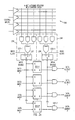
- FIG. 2 is a schematic diagram of one embodiment of a PLD constructed in accordance with the teachings of this invention, constructed as a single port register.
- a plurality of control input signals are applied to control input leads 201-1 through 201-N. These input signals are buffered by buffers 202-1 through 202-N in order to provide true and complement control input signals on leads 203-1 through 203-N and 204-1 through 204-N, respectively.
- a plurality of AND gates 207-1 through 207-M are used to provide signals resulting from their logical operation on a selected set of the true and complement input signals available on leads 203-1 through 203-N and 204-1 through 204-N.
- Each AND gate 207-1 through 207-M is shown as having an input bus 205-1 through 205-M. It is readily understood by those of ordinary skill in the art that this drawing illustrates a plurality of input signals for each AND gate, and the ability for the user to connect each input lead to a desired one of leads 203-1 through 203-N and 204-1 through 204-N.
- each AND gate 207-1 through 207-M can perform a logical AND function on any combination of a true and complement versions of the control input signals, depending of course upon the number of input leads associated with each such AND gate.
- the output signals from AND gates 207-1 through 207-M are applied to the input leads of OR gate 209 whose output signal serves, in this embodiment, as a write enable signal made available on lead 211.
- OR gate 209 is programmable, for example, utilizing a mask programmable circuit, fuse programmable circuit, or a register based array.
- the write enable signal is applied to the gating input leads of register 213 which contains register bits 213-1 through 213-P.
- the data input leads of register bits 213-1 through 213-P are connected to data input leads 214-1 through 214-P, respectively.
- register bits 213-1 through 213-P load input data from leads 214-1 through 214-P, respectively, upon control of the write enable signal generated by control input signals applied to control input leads 201-1 through 201-N without delaying the data input path. Since a write enable signal 211 is generated as a result of the specific programming of AND gates 207-1 through 207-M, great flexibility is provided in the ability to generate a write enable signal as a function of control input data.
- register bits 213-1 through 213-P can be either level sensitive or edge triggered, synchronous or asynchronous, as desired.
- read enable circuitry is provided in order to mask the output data from register bits 213-1 through 213-P to output leads 217-1 through 217-P.
- this read enable circuitry is simply a plurality of AND gates 216-1 through 216-P, each having one input lead connected to the data output lead of an associated one of register bits 213-1 through 213-P, and a second input lead connected to read enable lead 212, with its output lead serving as one of output leads 217-1 through 217-P of the data output bus.
- the read enable signal is generated in a similar manner as the write enable signal, although naturally a different set of programming criteria would be used to generate the read enable signal.
- NAND gates 216-1 through 216-P are replaced with transmission gates, as depicted in Figure 2a.
- the transmission gate may comprise, for example, an MOS transistor having its gate connected to the read enable line, and its source lead connected to the data output lead of its associated register bit and its drain lead connected to the data output bus.
- FIG. 2 shows a single write enable signal provided on write enable lead 211 for application to a plurality of register bits 213-1 through 213-P
- a plurality of write enable signals are generated for application to different ones or different subsets of register bits 213-1 through 213-P. In this manner, even greater flexibility is provided in that a number of different programmable control functions used to determine when data is to be latched into various register bits.
- Figure 2 shows a single read enable signal being made available on read enable line 212
- a plurality of read enable signals are provided in a similar fashion, providing a number of different programmable control functions, in order to enable different read enable signals to be applied to different ones or different subsets of data output masks 216-1 through 216-P.
- each write enable mask circuit 215-1 through 215-P is formed as an AND gate, similar to output mask circuits 216-1 through 216-P, and additional array elements are included in array 190 in order to provide one or more write enable masking signals for controlling all, individual ones, or specified subsets of write enable masking circuits 215-1 through 215-P.
- write enable masking circuits 215-1 through 215-P are controlled to provide one of three possible states: first, pass the write enable signal associated with the register bit unchanged; second, mask the write enable signal associated with the register bit so that the register is never write enabled; and thirdly, provide a write enable signal to the associated register bit regardless of the state of the write enable signal generated by array 190, thereby providing a transparent buffer.
- Figure 2b depicts an alternative embodiment of the circuit of Figure 2 which includes write gate 227, which receives a write enable gating signal on lead 227-1. This serves to allow selective write enable of register bits 213-1 through 213-P.
- read enable gate 228 receives a read enable gating signal on lead 228-1, allowing selective read enable of register bits 213-1 through 213-P.
- write enable gate 227 and read enable 228 may be used.
- either one or both of the write enable and read enable functions performed by subcircuits 298 and 299, respectively can be implemented utilizing more complex logic, including any desired number of input signals for generating the read enable and write enable signals.
- Figure 2c depicts an alternative embodiment of the circuit of Figure 2 which includes write enable latch 237, which receives a write clock signal on lead 237-1 in order to latch a read enable bit from control signal array 290 defining whether register bits 213-1 through 213-P are to be write enabled.
- read enable latch 238 receives a read enable clock signal on lead 238-1, and serves to latch a write enable bit from control signal array 290 indicating whether register bits 213-1 through 213-P are to be read enabled.
- write enable latch 237 and read enable latch 238 may be used.
- the use of write enable and read enable latches can be combined with additional logic in order to provide any desired type of read enable and write enable functions performed by subcircuits 295 and 296, respectively.
- Figure 3 is a schematic diagram depicting one embodiment of a multiple port register constructed in accordance with the teaching of this invention.
- the multiple port register of Figure 3 includes control signal array 390 which receives a plurality of control input signals and is programmed in order to provide a plurality of control output signals in response thereto.
- control signal array 390 provides output signals on control bus 315 which includes the following control signals: Register Write Enable A (WE A) Register Write Enable B (WE B) Register Read Enable A (RE A) Register Read Enable B (RE B)
- the embodiment of Figure 3 is a dual port register including input port A, output port A, input port B, and output port B, each input and output port including P input or output leads, respectively.
- the embodiment of Figure 3 includes register 313 which is P bits wide and includes register bits 313-1 through 313-P, each receiving a corresponding input data signal (DA) from input port A and a corresponding input data signal (DB) from input port B.
- Each register bit 313-1 through 313-P also includes enable input A (GA) which receives the write register A enable (WE A) signal from control signal array 390, the enable input B (GB) which receives the write register B enable (WE B) signal from control signal array 390.
- Registers 313-1 through 313-P also include a Q output lead which provides the data output signal to the selected one of the A and B output leads associated with that register bit, as selected by read A enable circuitry 333-1a through 333-Pa and read B enable circuitry 333-1b through 333-Pb, which receive the read register A enable (RE A) and read register B (RE B) enable signals, respectively, from control signal array 390.
- the multiple port register of Figure 3 can be expanded with equal applicability to provide any desired number of ports.
- the number of write ports and the number of read ports need not be equal.
- read enable circuitry 333 can be implemented in other manners, for example, by utilizing a plurality of transmission gates as depicted in the embodiment of Figure 3a. Any number of single port implementations constructed in accordance with the teachings of this invention, or indeed combinations of various types of single port implementations constructed in accordance with the teachings of this invention, may be conveniently combined in order form a device having a plurality of read and/or write ports.
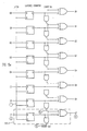
- Figure 4 is a schematic diagram of one embodiment of this invention which is a multiple port register file , i.e. a circuit including a plurality of input and output ports and a plurality of registers, each being P bits wide and receiving independent read and write enable control signals from control signal array 490.
- the multiple port register of Figure 4 includes control signal array 490 which receives a plurality of control input signals and is programmed in order to provide a plurality of control output signals in response thereto.
- control signal array 490 provides output signals on control bus 415 which includes the following control signals for both register 0 and register 1: Register Write Enable A (WE A) Register Write Enable B (WE B) Register Read Enable A (RE A) Register Read Enable B (RE B)
- register 0 and register 1 Register Write Enable A
- WE A Register Write Enable B
- RE A Register Read Enable B
- the embodiment of Figure 4 provides two P-bit dual port registers, each register including input port A, output port A, input port B, and output port B, each input and output port including P input or output leads, respectively.
- the embodiment of Figure 4 includes register 413 which is P bits wide and includes register bits 413-1 through 413-P, each receiving a corresponding input data signal (DA) from input port A and a corresponding input data signal (DB) from input port B.
- Each register bit 413-1 through 413-P also includes enable input A (GA) which receives the write register A enable (WE A) signal from control signal array 490, the enable input B (GB) which receives the write register B enable (WE B) signal from control signal array 490.
- Registers 413-1 through 413-P also include a Q output lead which provides the data output signal to the selected one of the A and B output leads associated with that register bit, as selected by read A enable circuitry 433-1a through 433-Pa and read B enable circuitry 433-1b through 433-Pb, which receive the read register A enable (RE A) and read register B (RE B) enable signals, respectively, from control signal array 490.
- Register 414 operates in a similar fashion as register 413.
- the output signals from the selected output port of register 413 are ORed with the selected output signals from register 414 by OR gates 415-1a through 415-Pa and 415-1b through 415-Pb.
- OR gate array 415 is replaced with a plurality of transmission gates, as depicted in Figure 4a, in order to select the appropriate data for application to each output data bus.
- the output signals from registers 413 and 414 are applied to separate output leads.
- the output signals are selected in any other desired manner, for example, by utilizing multiplexors.
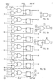
- FIG. 5 is a schematic diagram of one embodiment of this invention in which register 213 of the embodiment of Figure 2 is replaced by a plurality of general logic/storage function elements 513-1 through 513-P.
- Each logic/storage function element 513-1 through 513-P has data input leads 514-1 through 514-P, data output leads 526-1 through 526-P, a first set (527-1 through 527-P+1) and a second set (528-1 through 528-P+1) of serial data input/output leads or control input/status output leads, which serve to connect logic/storage function elements 513-1 through 513-P in a serial fashion.
- Each logic/storage function element 513-1 through 513-P also includes a first global control signal input lead 511 and a second global control signal input lead 512.
- first global control signal input lead 511 also includes a first global control signal input lead 511 and a second global control signal input lead 512.
- second global control signal input lead 512 may be utilized in each logic/storage function element 513-1 through 513-P, or that different numbers may be associated with different ones of logic/storage function elements 513-1 through 513-P.
- Logic/storage function element 513-1 shows its eight leads labeled as 1 through 8 for ease in understanding how the specific examples of logic/storage function elements shown in Figures 5a through 5g are implemented in the embodiment of Figure 5.
- logic/storage function elements 513-1 through 513-P comprise simple buffers which are controlled by one or more global control signals, as depicted in Figure 5a. This embodiment provides programmable control of a unidirectional buffer.
- each logic/storage function elements 513-1 through 513-P includes two data input leads 2a and 2b, each serving as an input lead similar to lead 2 of logic/storage function element 513-1 of Figure 5.
- Exclusive OR gate 591 allows comparison of two input bits applied to input leads 2a and 2b and provides the result on data output lead 4 of the logic/storage function element.
- a single data input lead 2 is used with register 592 contained within logic/storage function element such that a first bit to be compared is loaded into register 592 and compared with data subsequently input on data input lead 2 by exclusive OR gate 593.
- Figure 5d depicts an alternative embodiment of this invention, in which each logic/storage element includes a register capable of storing data which is loaded in parallel to the logic/storage elements. This data is capable of being shifted to adjacent logic/storage function elements under control of the global control signals. In this manner, this embodiment serves as a programmable parallel loadable and readable shift register.
- Figure 5e depicts an alternative embodiment of logic/storage elements suitable for use in the embodiment of Figure 5.
- the logic/storage element of Figure 5e allows the embodiment of Figure 5 to serve as a latched counter with ripple-carry output.
- Figure 5f depicts an alternative embodiment of logic/storage elements constructed in accordance with teachings of this invention which allows the embodiment of Figure 5 to serve as a 2:1 multiplexor.
- Figure 5g depicts logic/storage element suitable for use in the embodiment of Figure 5.
- Each logic/storage element of Figure 5g serves as a universal, 2 input logic element which provides a logical operation on the 2 input signals received on input leads 2a and 2b in accordance with the control signals provided on control leads 1a through 1d, according to the following Truth Table.
- each of the various embodiments described in this specification can include, if desired, write or control masking circuits similar to write enable masking circuits 115-1 through 115-P of the embodiment of Figure 2.
- Alternative embodiments include means for feeding back output signals from the data register to the input of the control array.
- any type of logical function can be placed between the output of the data register, the input of the data register, the input of the control array, and the output of the control array in order to derive any desired operating parameters.
- Such a logical function can include parity generation and checking of the data in the data path.
- tag bits can be utilized, in which a tag bit register is used in addtion to the data register and, if desired, controlled in a manner different than how the data register is controlled.
Landscapes
- Engineering & Computer Science (AREA)
- Physics & Mathematics (AREA)
- Mathematical Physics (AREA)
- General Engineering & Computer Science (AREA)
- Computer Hardware Design (AREA)
- Computing Systems (AREA)
- Software Systems (AREA)
- Theoretical Computer Science (AREA)
- General Physics & Mathematics (AREA)
- Logic Circuits (AREA)
Applications Claiming Priority (2)
| Application Number | Priority Date | Filing Date | Title |
|---|---|---|---|
| US07/504,967 US5055712A (en) | 1990-04-05 | 1990-04-05 | Register file with programmable control, decode and/or data manipulation |
| US504967 | 1990-04-05 |
Publications (2)
| Publication Number | Publication Date |
|---|---|
| EP0450616A2 true EP0450616A2 (fr) | 1991-10-09 |
| EP0450616A3 EP0450616A3 (en) | 1992-05-20 |
Family
ID=24008467
Family Applications (1)
| Application Number | Title | Priority Date | Filing Date |
|---|---|---|---|
| EP19910105328 Withdrawn EP0450616A3 (en) | 1990-04-05 | 1991-04-04 | Register file with programmable control, decode and/or data manipulation |
Country Status (3)
| Country | Link |
|---|---|
| US (1) | US5055712A (fr) |
| EP (1) | EP0450616A3 (fr) |
| JP (1) | JPH0730407A (fr) |
Families Citing this family (8)
| Publication number | Priority date | Publication date | Assignee | Title |
|---|---|---|---|---|
| KR930004033B1 (ko) * | 1990-08-09 | 1993-05-19 | 현대전자산업 주식회사 | 프로그래머블 로직소자의 입력/출력 마크로셀 |
| US5250859A (en) * | 1991-09-27 | 1993-10-05 | Kaplinsky Cecil H | Low power multifunction logic array |
| US5719889A (en) * | 1995-12-20 | 1998-02-17 | International Business Machines Corporation | Programmable parity checking and comparison circuit |
| US6150836A (en) * | 1997-06-13 | 2000-11-21 | Malleable Technologies, Inc. | Multilevel logic field programmable device |
| US6006321A (en) | 1997-06-13 | 1999-12-21 | Malleable Technologies, Inc. | Programmable logic datapath that may be used in a field programmable device |
| US6654870B1 (en) * | 1999-06-21 | 2003-11-25 | Pts Corporation | Methods and apparatus for establishing port priority functions in a VLIW processor |
| US6438569B1 (en) | 1999-09-20 | 2002-08-20 | Pmc-Sierra, Inc. | Sums of production datapath |
| US10802754B2 (en) * | 2018-03-12 | 2020-10-13 | Micron Technology, Inc. | Hardware-based power management integrated circuit register file write protection |
Family Cites Families (30)
| Publication number | Priority date | Publication date | Assignee | Title |
|---|---|---|---|---|
| US3569685A (en) * | 1968-07-11 | 1971-03-09 | Fairchild Camera Instr Co | Precision controlled arithmetic processing system |
| US3593317A (en) * | 1969-12-30 | 1971-07-13 | Ibm | Partitioning logic operations in a generalized matrix system |
| US3849638A (en) * | 1973-07-18 | 1974-11-19 | Gen Electric | Segmented associative logic circuits |
| US3949370A (en) * | 1974-06-06 | 1976-04-06 | National Semiconductor Corporation | Programmable logic array control section for data processing system |
| US4034356A (en) * | 1975-12-03 | 1977-07-05 | Ibm Corporation | Reconfigurable logic array |
| US4124899A (en) * | 1977-05-23 | 1978-11-07 | Monolithic Memories, Inc. | Programmable array logic circuit |
| JPS6053907B2 (ja) * | 1978-01-27 | 1985-11-27 | 日本電気株式会社 | 二項ベクトル乗算回路 |
| US4233667A (en) * | 1978-10-23 | 1980-11-11 | International Business Machines Corporation | Demand powered programmable logic array |
| FR2440657A1 (fr) * | 1978-10-31 | 1980-05-30 | Ibm France | Perfectionnement aux reseaux logiques programmables a fonctions multiples |
| US4293783A (en) * | 1978-11-01 | 1981-10-06 | Massachusetts Institute Of Technology | Storage/logic array |
| US4482953A (en) * | 1980-05-30 | 1984-11-13 | Fairchild Camera & Instrument Corporation | Computer with console addressable PLA storing control microcode and microinstructions for self-test of internal registers and ALU |
| US4495590A (en) * | 1980-12-31 | 1985-01-22 | International Business Machines Corporation | PLA With time division multiplex feature for improved density |
| US4422072A (en) * | 1981-07-30 | 1983-12-20 | Signetics Corporation | Field programmable logic array circuit |
| JPS5885638A (ja) * | 1981-11-17 | 1983-05-23 | Ricoh Co Ltd | プログラマブルロジツクアレイ |
| US4409683A (en) * | 1981-11-18 | 1983-10-11 | Burroughs Corporation | Programmable multiplexer |
| US4660171A (en) * | 1981-12-21 | 1987-04-21 | International Business Machines Corp. | Apparatus and method using a programmable logic array for decoding an operation code and providing a plurality of sequential output states |
| US4506173A (en) * | 1982-10-25 | 1985-03-19 | Burroughs Corporation | Low power partitioned PLA |
| JPS6095651A (ja) * | 1983-10-31 | 1985-05-29 | Toshiba Corp | 記憶装置 |
| US4551815A (en) * | 1983-12-12 | 1985-11-05 | Aerojet-General Corporation | Functionally redundant logic network architectures with logic selection means |
| US4742252A (en) * | 1985-03-29 | 1988-05-03 | Advanced Micro Devices, Inc. | Multiple array customizable logic device |
| US4807183A (en) * | 1985-09-27 | 1989-02-21 | Carnegie-Mellon University | Programmable interconnection chip for computer system functional modules |
| US4703206A (en) * | 1985-11-19 | 1987-10-27 | Signetics Corporation | Field-programmable logic device with programmable foldback to control number of logic levels |
| US4734876A (en) * | 1985-12-18 | 1988-03-29 | Motorola, Inc. | Circuit for selecting one of a plurality of exponential values to a predetermined base to provide a maximum value |
| JPS62194540A (ja) * | 1986-02-21 | 1987-08-27 | Toshiba Corp | ディジタル信号処理回路 |
| US4675556A (en) * | 1986-06-09 | 1987-06-23 | Intel Corporation | Binomially-encoded finite state machine |
| US4791603A (en) * | 1986-07-18 | 1988-12-13 | Honeywell Inc. | Dynamically reconfigurable array logic |
| US4829425A (en) * | 1986-10-21 | 1989-05-09 | Intel Corporation | Memory-based interagent communication mechanism |
| US4803622A (en) * | 1987-05-07 | 1989-02-07 | Intel Corporation | Programmable I/O sequencer for use in an I/O processor |
| US4811296A (en) * | 1987-05-15 | 1989-03-07 | Analog Devices, Inc. | Multi-port register file with flow-through of data |
| US4996661A (en) * | 1988-10-05 | 1991-02-26 | United Technologies Corporation | Single chip complex floating point numeric processor |
-
1990
- 1990-04-05 US US07/504,967 patent/US5055712A/en not_active Expired - Lifetime
-
1991
- 1991-04-04 EP EP19910105328 patent/EP0450616A3/en not_active Withdrawn
- 1991-04-05 JP JP3154169A patent/JPH0730407A/ja active Pending
Also Published As
| Publication number | Publication date |
|---|---|
| US5055712A (en) | 1991-10-08 |
| EP0450616A3 (en) | 1992-05-20 |
| JPH0730407A (ja) | 1995-01-31 |
Similar Documents
| Publication | Publication Date | Title |
|---|---|---|
| US6014038A (en) | Function block architecture for gate array | |
| US5046035A (en) | High-performance user programmable logic device (PLD) | |
| US5121006A (en) | Registered logic macrocell with product term allocation and adjacent product term stealing | |
| US5646544A (en) | System and method for dynamically reconfiguring a programmable gate array | |
| US7843215B2 (en) | Reconfigurable array to compute digital algorithms | |
| US5394031A (en) | Apparatus and method to improve programming speed of field programmable gate arrays | |
| US7193433B1 (en) | Programmable logic block having lookup table with partial output signal driving carry multiplexer | |
| US5742180A (en) | Dynamically programmable gate array with multiple contexts | |
| US5761099A (en) | Programmable logic array integrated circuits with enhanced carry routing | |
| EP0081917B1 (fr) | Multiplexeur programmable | |
| US9461650B2 (en) | User registers implemented with routing circuits in a configurable IC | |
| US7218143B1 (en) | Integrated circuit having fast interconnect paths between memory elements and carry logic | |
| US5371422A (en) | Programmable logic device having multiplexers and demultiplexers randomly connected to global conductors for interconnections between logic elements | |
| US4918641A (en) | High-performance programmable logic device | |
| US7804719B1 (en) | Programmable logic block having reduced output delay during RAM write processes when programmed to function in RAM mode | |
| US20050218929A1 (en) | Field programmable gate array logic cell and its derivatives | |
| US7268587B1 (en) | Programmable logic block with carry chains providing lookahead functions of different lengths | |
| GB2318663A (en) | Hierarchical interconnect for programmable logic devices | |
| US6043676A (en) | Wide exclusive or and wide-input and for PLDS | |
| US5055712A (en) | Register file with programmable control, decode and/or data manipulation | |
| US7265576B1 (en) | Programmable lookup table with dual input and output terminals in RAM mode | |
| US7205790B1 (en) | Programmable integrated circuit providing efficient implementations of wide logic functions | |
| US7215138B1 (en) | Programmable lookup table with dual input and output terminals in shift register mode | |
| US7199610B1 (en) | Integrated circuit interconnect structure having reduced coupling between interconnect lines | |
| US5936426A (en) | Logic function module for field programmable array |
Legal Events
| Date | Code | Title | Description |
|---|---|---|---|
| PUAI | Public reference made under article 153(3) epc to a published international application that has entered the european phase |
Free format text: ORIGINAL CODE: 0009012 |
|
| AK | Designated contracting states |
Kind code of ref document: A2 Designated state(s): DE FR GB IT |
|
| RIN1 | Information on inventor provided before grant (corrected) |
Inventor name: LEUNG, FREDERICK KWOK YIN Inventor name: PICKETT, SCOTT KINNEY Inventor name: HAWLEY, DAVID WARREN |
|
| PUAL | Search report despatched |
Free format text: ORIGINAL CODE: 0009013 |
|
| AK | Designated contracting states |
Kind code of ref document: A3 Designated state(s): DE FR GB IT |
|
| 17P | Request for examination filed |
Effective date: 19920708 |
|
| 17Q | First examination report despatched |
Effective date: 19950207 |
|
| STAA | Information on the status of an ep patent application or granted ep patent |
Free format text: STATUS: THE APPLICATION IS DEEMED TO BE WITHDRAWN |
|
| 18D | Application deemed to be withdrawn |
Effective date: 19950620 |