EP0450941A2 - Anzeigevorrichtung mit aktiver Matrix - Google Patents
Anzeigevorrichtung mit aktiver Matrix Download PDFInfo
- Publication number
- EP0450941A2 EP0450941A2 EP91302937A EP91302937A EP0450941A2 EP 0450941 A2 EP0450941 A2 EP 0450941A2 EP 91302937 A EP91302937 A EP 91302937A EP 91302937 A EP91302937 A EP 91302937A EP 0450941 A2 EP0450941 A2 EP 0450941A2
- Authority
- EP
- European Patent Office
- Prior art keywords
- pixel electrodes
- pixel
- display device
- electrode
- insulating layer
- Prior art date
- Legal status (The legal status is an assumption and is not a legal conclusion. Google has not performed a legal analysis and makes no representation as to the accuracy of the status listed.)
- Granted
Links
Images



Classifications
-
- G—PHYSICS
- G02—OPTICS
- G02F—OPTICAL DEVICES OR ARRANGEMENTS FOR THE CONTROL OF LIGHT BY MODIFICATION OF THE OPTICAL PROPERTIES OF THE MEDIA OF THE ELEMENTS INVOLVED THEREIN; NON-LINEAR OPTICS; FREQUENCY-CHANGING OF LIGHT; OPTICAL LOGIC ELEMENTS; OPTICAL ANALOGUE/DIGITAL CONVERTERS
- G02F1/00—Devices or arrangements for the control of the intensity, colour, phase, polarisation or direction of light arriving from an independent light source, e.g. switching, gating or modulating; Non-linear optics
- G02F1/01—Devices or arrangements for the control of the intensity, colour, phase, polarisation or direction of light arriving from an independent light source, e.g. switching, gating or modulating; Non-linear optics for the control of the intensity, phase, polarisation or colour
- G02F1/13—Devices or arrangements for the control of the intensity, colour, phase, polarisation or direction of light arriving from an independent light source, e.g. switching, gating or modulating; Non-linear optics for the control of the intensity, phase, polarisation or colour based on liquid crystals, e.g. single liquid crystal display cells
- G02F1/133—Constructional arrangements; Operation of liquid crystal cells; Circuit arrangements
- G02F1/136—Liquid crystal cells structurally associated with a semi-conducting layer or substrate, e.g. cells forming part of an integrated circuit
- G02F1/1362—Active matrix addressed cells
- G02F1/136227—Through-hole connection of the pixel electrode to the active element through an insulation layer
-
- G—PHYSICS
- G02—OPTICS
- G02F—OPTICAL DEVICES OR ARRANGEMENTS FOR THE CONTROL OF LIGHT BY MODIFICATION OF THE OPTICAL PROPERTIES OF THE MEDIA OF THE ELEMENTS INVOLVED THEREIN; NON-LINEAR OPTICS; FREQUENCY-CHANGING OF LIGHT; OPTICAL LOGIC ELEMENTS; OPTICAL ANALOGUE/DIGITAL CONVERTERS
- G02F1/00—Devices or arrangements for the control of the intensity, colour, phase, polarisation or direction of light arriving from an independent light source, e.g. switching, gating or modulating; Non-linear optics
- G02F1/01—Devices or arrangements for the control of the intensity, colour, phase, polarisation or direction of light arriving from an independent light source, e.g. switching, gating or modulating; Non-linear optics for the control of the intensity, phase, polarisation or colour
- G02F1/13—Devices or arrangements for the control of the intensity, colour, phase, polarisation or direction of light arriving from an independent light source, e.g. switching, gating or modulating; Non-linear optics for the control of the intensity, phase, polarisation or colour based on liquid crystals, e.g. single liquid crystal display cells
- G02F1/133—Constructional arrangements; Operation of liquid crystal cells; Circuit arrangements
- G02F1/136—Liquid crystal cells structurally associated with a semi-conducting layer or substrate, e.g. cells forming part of an integrated circuit
- G02F1/1362—Active matrix addressed cells
- G02F1/136213—Storage capacitors associated with the pixel electrode
-
- H—ELECTRICITY
- H10—SEMICONDUCTOR DEVICES; ELECTRIC SOLID-STATE DEVICES NOT OTHERWISE PROVIDED FOR
- H10D—INORGANIC ELECTRIC SEMICONDUCTOR DEVICES
- H10D86/00—Integrated devices formed in or on insulating or conducting substrates, e.g. formed in silicon-on-insulator [SOI] substrates or on stainless steel or glass substrates
-
- G—PHYSICS
- G02—OPTICS
- G02F—OPTICAL DEVICES OR ARRANGEMENTS FOR THE CONTROL OF LIGHT BY MODIFICATION OF THE OPTICAL PROPERTIES OF THE MEDIA OF THE ELEMENTS INVOLVED THEREIN; NON-LINEAR OPTICS; FREQUENCY-CHANGING OF LIGHT; OPTICAL LOGIC ELEMENTS; OPTICAL ANALOGUE/DIGITAL CONVERTERS
- G02F1/00—Devices or arrangements for the control of the intensity, colour, phase, polarisation or direction of light arriving from an independent light source, e.g. switching, gating or modulating; Non-linear optics
- G02F1/01—Devices or arrangements for the control of the intensity, colour, phase, polarisation or direction of light arriving from an independent light source, e.g. switching, gating or modulating; Non-linear optics for the control of the intensity, phase, polarisation or colour
- G02F1/13—Devices or arrangements for the control of the intensity, colour, phase, polarisation or direction of light arriving from an independent light source, e.g. switching, gating or modulating; Non-linear optics for the control of the intensity, phase, polarisation or colour based on liquid crystals, e.g. single liquid crystal display cells
- G02F1/133—Constructional arrangements; Operation of liquid crystal cells; Circuit arrangements
- G02F1/136—Liquid crystal cells structurally associated with a semi-conducting layer or substrate, e.g. cells forming part of an integrated circuit
- G02F1/13606—Liquid crystal cells structurally associated with a semi-conducting layer or substrate, e.g. cells forming part of an integrated circuit having means for reducing parasitic capacitance
-
- G—PHYSICS
- G02—OPTICS
- G02F—OPTICAL DEVICES OR ARRANGEMENTS FOR THE CONTROL OF LIGHT BY MODIFICATION OF THE OPTICAL PROPERTIES OF THE MEDIA OF THE ELEMENTS INVOLVED THEREIN; NON-LINEAR OPTICS; FREQUENCY-CHANGING OF LIGHT; OPTICAL LOGIC ELEMENTS; OPTICAL ANALOGUE/DIGITAL CONVERTERS
- G02F1/00—Devices or arrangements for the control of the intensity, colour, phase, polarisation or direction of light arriving from an independent light source, e.g. switching, gating or modulating; Non-linear optics
- G02F1/01—Devices or arrangements for the control of the intensity, colour, phase, polarisation or direction of light arriving from an independent light source, e.g. switching, gating or modulating; Non-linear optics for the control of the intensity, phase, polarisation or colour
- G02F1/13—Devices or arrangements for the control of the intensity, colour, phase, polarisation or direction of light arriving from an independent light source, e.g. switching, gating or modulating; Non-linear optics for the control of the intensity, phase, polarisation or colour based on liquid crystals, e.g. single liquid crystal display cells
- G02F1/133—Constructional arrangements; Operation of liquid crystal cells; Circuit arrangements
- G02F1/136—Liquid crystal cells structurally associated with a semi-conducting layer or substrate, e.g. cells forming part of an integrated circuit
- G02F1/1362—Active matrix addressed cells
- G02F1/1368—Active matrix addressed cells in which the switching element is a three-electrode device
- G02F1/13685—Top gates
Definitions
- the present invention relates to an active matrix display device, and more particularly to an active matrix display device employing a switching device such as a thin film transistor (hereinafter called "TFT"), and using liquid crystal for a display medium.
- TFT thin film transistor
- LCD liquid crystal display devices
- Such research is producing successful models.
- the research on active matrix LCDs are divided into at least two types depending upon the objects: one is to achieve a large display screen usable for a wall-hung TV display, and the other is to achieve a high-precision display screen, A high-precision, small-size display screen is particularly in strong demand so as to achieve a color view finder for video cameras.
- the active matrix LCD is provided with IC chips for driving a TFT array.
- the terminals are provided at such small distances so as to make it difficult to mount IC chips thereon.
- a TFT array is formed on the substrate for constituting a driving circuit.
- a basic structure of an active matrix display device using a driving circuit and a TFT array both formed on the same substrate will be described.
- a gate driving circuit 54 On a substrate 50 are disposed a gate driving circuit 54, a source driving circuit 55, and a TFT array section 53 in which multiple gate buses 51 in parallel extend from the gate driving circuit 54.
- Multiple source buses 52 from the source driving circuit 55 cross the gate buses 51 at right angles.
- an additional capacitor common line 59 is disposed.
- a rectangular region enclosed by the source buses 52, the gate buses 51 and the additional capacitor common line 59 includes the TFT 56, pixels 57 and additional capacitors 58.
- the gate electrode of the TFT 56 is connected to the gate bus 51, and the source electrode is connected to the source bus 52.
- Liquid crystal is confined in between the pixel electrode connected to the drain electrode of the TFT 56 and the counter electrode on the substrate so as to constitute pixels 57.
- An additional capacitor 58 is disposed between the TFT 56 and the additional capacitor common line 59.
- the additional capacitor common line 59 is connected to an electrode having the same potential as that of the counter electrode.
- the gate driving circuit 54 In this type of display the gate driving circuit 54 generates a signal in response to which the TFT 56 connected to the gate bus 51 is turned on.
- the source driving circuit 55 sends an image signal to the pixels 57 through the source bus 52.
- the image signal is retained between the pixel electrodes and the counter electrode. Since a high-precision, small-size active matrix LCD has pixels having a reduced area, the capacitance between the pixel electrodes and the counter electrodes becomes small. As a result, the image signal cannot be retained for a required period of time.
- the potential of the bus varies in large amplitude, thereby failing to match with the potential of the pixel electrode.
- the additional capacitors 58 are provided in parallel with the pixels 57.
- One of the terminals of each capacitor 58 is connected to the drain electrode of the TFT 56, and the other terminal is connected to an electrode having the same potential as that of the counter electrode through the additional capacitor common line 59 so as to equalize the potentials between the other terminal of the TFT 56 and the counter electrode.
- the active matrix display devices incorporating the driving circuit as a unit uses polysilicon for a semiconductor layer of the TFT because of the high degree of mobility of electrons and holes, and of the possibility of fabricating n-type TFTs and p-type TFTs, thereby making it possible to constitute a CMOS construction.
- This type of active matrix display device is disadvantageous in that the provision of additional capacitors reduces the effective area for the pixel electrodes, thereby lowering the numerical aperture of the display panel as a whole.
- Japanese Laid-Open Patent Publication No. 1-304402 proposes an active matrix display device, which includes an additional capacitor common line.
- a polysilicon layer is formed on a glass substrate 11 by a known method such as a CVD method and a sputtering method.
- the resulting polysilicon layer is patterned so as to form a semiconductor layer 12 and a lower capacitor electrode 5.
- a gate insulating layer 13 is formed by a CVD method or by thermally oxidizing the surface of the polysilicon layer.
- the lower capacitor electrode 5 is subjected to doping by an ion implantation method so as to make it a low resistance capacitor electrode.
- the gate bus 1, the gate electrodes 3a, and 3b, an upper capacitor electrode 6 are formed with n-type or p-type polysilicon.
- the additional capacitor 27 is formed between the upper capacitor electrode 6 and the lower capacitor electrode 5.
- lower parts below the gate electrodes 3a and 3b of the semiconductor layer 12 are subjected to ion implantation. In this way the source and drain region of the TFT is formed as a self-alignment structure.
- An insulating layer 14 is formed on the whole surface of the substrate 11.
- the contact holes 7a and 7b extend through the insulating layer 14 and the gate insulating layer 13, and are open on the semiconductor layer 12 and the lower capacitor electrode 5.
- the source bus 2 and the additional capacitor common line 8 are simultaneously formed with a low-resistance metal such as aluminum.
- a low-resistance metal such as aluminum.
- the source bus 2 is formed such that it expands on the contact hole 7a
- the additional capacitor common line 8 is formed such that it expands on the contact hole 7c.
- the source bus 2 is connected to the semiconductor layer 12 through the contact hole 7a
- the additional capacitor common line 8 is connected to the upper capacitor electrode 6 through the contact hole 7c.
- the additional capacitor common line 8 is connected to an electrode having the same potential as that of the counter electrode on the counter substrate.
- Figure 5 further illustrates that a pixel electrode 4 of Indium Tin Oxide (ITO) is patterned. Part of the pixel electrode 4 extends through the contact hole 7b, thereby connecting the pixel electrode 4 to the semiconductor layer 12 through the contact hole 7b. The whole surface of the substrate 11 is covered with a protective layer 15.
- ITO Indium Tin Oxide
- the additional capacitor 27 has a thin gate insulating layer 13 between the upper capacitor electrode 6 and the lower capacitor electrode 5, thereby increasing the capacitance of the additional capacitor 27 per unit area.
- the area occupied by the additional capacitor 27 is advantageously minimized, thereby preventing the numerical aperture of the display panel from being reduced.
- the size of the pixel electrodes In order to enhance the high-precision display, it is necessary to minimize the size of the pixel electrodes. However, if the size of the pixel electrodes is reduced beyond a particular limit, the spacing of the gate bus 1 and the source bus 2, the size of the TFT 25a and 25b cannot be shortened any more. As a result, the numerical aperture of the display panel become low, thereby resulting in a dark image picture.
- the brightness of the image picture on the display screen is not always proportional to the area of the pixel electrodes 4.
- the liquid crystal layer positioning on the pixel electrodes 4 unavoidably has an electric field whose intensity depends upon the degree of display, and the molecules therein are orientated by the electric field, but the liquid crystal positioning off the pixel electrodes 4 has no electric field, so that the molecules are in disorder.
- the normal-white system In the twisted nematic mode that is currently in commonest use, the normal-white system is used because it is least liable to birefringent when an image picture is represented white. Under the normal-white system the "white" representation occurs in other area having no electric field than the pixel electrodes 4. As a result, the contrast ratio decreases.
- a light shield layer is formed in other areas than the parts on the counter substrate corresponding to the pixel electrodes,
- the light shield layer is in principle effective to prevent the contrast ratio from decreasing but the actuality is that the numerical aperture of the display panel is nevertheless reduced because of the overlapping of the edges of the light shield layer and the peripheral edge of the pixel electrode.
- the known high-precision, small-size active matrix display device reduces the display performance because of the low numerical aperture.
- a display device having a large area covered by the light shield layer is used for a projection type display device, another problem arises as black spots in the image picture resulting from the light shield layers.
- the active matrix display device of this invention which overcomes the above-discussed and numerous other disadvantages and deficiencies of the prior art, comprises a first insulated substrate and a second insulated substrate, pixel electrodes arranged in matrix on an inner side of the first insulated substrate, signal lines for supplying an image signal, the signal line connecting one pixel electrode to another, wherein the signal line is covered with an insulating layer, and the pixel electrodes are formed on the insulating layers.
- the parts of the pixel electrodes overlay parts of the signal lines through the insulating layers.
- the active matrix display device comprises a pair of insulating substrates, pixel electrodes arranged in matrix on an inner side of one of the substrates, signal lines for supplying an image signal, the signal line connecting one pixel electrode to another, an additional capacitor for retaining the electric charge of the pixel electrode, an additional capacitor common line connected to one electrode of the additional capacitor, wherein the signal line is covered with an insulating layer, and the pixel electrodes are formed on the insulating layers, and wherein parts of the pixel electrodes overlay parts of the additional capacitor common lines.
- the second insulated substrate comprises a stagger type thin film transistor including a semiconductor layer, a gate insulating layer, and a gate electrode formed thereon, the thin film transistor having a source electrode connected to the signal line, and a drain electrode connected to the pixel electrodes.
- the present invention described herein makes possible of the objective of providing an active matrix display device capable of reproducing a high-precision image picture on the display by using pixel electrodes having a relatively large area and a large numerical aperture.
- the signal line or the additional capacitor common line or both are wholly covered with an insulating layer on which the pixel electrodes are formed.
- the present invention ensures that no leakage of light occurs between the signal lines and the pixel electrodes or between the additional capacitor common lines and the pixel electrodes, thereby eliminating the necessity of providing light shield layers in these interface areas. This also increases the numerical aperture of the display panel.
- a transmissive insulating substrate 11 such as quartz and glass was covered with a polysilicon thin layer by a CVD method.
- the polysilicon thin layer is used to make a semiconductor layer 12 and a lower capacitor electrode 5 at a later stage.
- a stagger type TFT was used.
- an insulating layer was formed by a CVD method, but it can be done by other methods such as by sputtering or by thermally oxidizing the surface of the polysilicon thin layer.
- the insulating layer is used to make a gate insulating layer 13 at a later stage.
- the gate insulating layer 13 was approximately 100 nm thick.
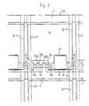
- the semiconductor layer 12 and the lower capacitor electrode 5 were patterned into the shape shown in Figure 1.
- the gate insulating layer 13 can be formed after the semiconductor layer 12 and the lower capacitor electrode 5 are patterned into the desired shapes. It is possible to anneal it by laser or anneal it in a nitrogen atmosphere before the formation of the insulating layer, so as to enhance the crystallization of the polysilicon layer. Then, ion was implanted in the lower capacitor electrode 5 so as to make it a low resistance lower capacitor electrode.
- the gate bus 1, the gate electrode 3a and 3b, and the upper capacitor electrode 6 were formed.
- a polysilicon thin layer was formed by a CVD method, and subjected to doping.
- the polysilicon thin layer was patterned into the shapes shown in Figure 1.
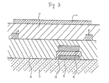
- An additional capacitor 27 was formed between the upper capacitor electrode 6 and the lower capacitor electrode 5.
- the gate electrodes 3a and 3b, and a resist formed by photolithography were used as a mask, and under this mask ion was implanted in the parts of the semiconductor layer 12 lower than the gate electrodes 3a and 3b. In this way the source drain regions of the TFTs 25a and 25b were formed.
- the whole surface of the substrate 11 was covered with an insulating layer 14 by a CVD method, in the form of a silicon oxidized film or a silicon nitride film either having a thickness of 700 nm. Then, as shown in Figure 1 two contact holes 7a and 7b were formed.
- the addition of impurity to the silicon oxidized film facilitates the flattening of the top surface of the insulating layer 14 at about 1000°C.
- the flat surface of the insulating layer 14 prevents the wires formed thereon from being broken.
- the contact hole 7a extended through the insulating layer 14 and the gate insulating layer 13, and is open on the semiconductor layer 12.
- the contact hole 7c extended through the insulating layer 14 and is open on an end portion of the upper capacitor electrode 6.
- the source bus 2 functioning as a signal line, and the additional capacitor common line 8 were simultaneously formed by using a low resistance metal such as aluminum. As shown in Figure 1, the source bus 2 was passed through the contact hole 7a and expanded in the opening thereof. The additional capacitor common line 8 was passed through the contact hole 7c and expanded in the opening thereof. In this way the source bus 2 was connected to the semiconductor layer 12 through the contact hole 7a. The additional capacitor common line 8 was connected to the upper capacitor electrode 6 through the contact hole 7c. After the display device was finished, the additional capacitor common line 8 was connected to an electrode having the same potential as that of the counter electrode on the counter substrate.
- the silicon oxidizing film or silicon nitride film was formed on the whole surface of the substrate 11 by a CVD method, so as to form an intermediate insulating layer 17 in which a contact hole 7b was formed.
- the contact hole 7b extended through the intermediate insulating layer 17, the insulating layer 14 and the gate insulating layer 13 and was open on the semiconductor layer 12 and the lower capacitor electrode 5.
- a pixel electrode 4 was formed with ITO by patterning. As shown in Figure 1, the pixel electrode 4 was formed so as to overlay the source bus 2 and the additional capacitor common line 8 and the contact hole 7b and 7c, and the additional capacitor 27. The pixel electrode 4 was connected to the semiconductor layer 12 through the contact hole 7b.
- the pixel electrodes 4 and the source bus 2, and the pixel electrode 4 and the additional capacitor common line 8 were layered through the intermediate insulating layer 17.
- This arrangement allows the pixel electrode 4 to be formed by patterning without regard to the distance from the source bus 2 and the additional capacitor common line 8, thereby securing a display device with a relatively large numerical aperture. No leakage of light occurs between the pixel electrode 4 and the source bus 2, or between the pixel electrode 4 and the additional capacitor common line 8. It is therefore unnecessary to overlap light shield layers on these interface areas, thereby avoiding reducing the numerical aperture of the display panel.
- the light shield layers are provided at the areas between the source bus 2 and the additional capacitor common line 8. The width of the light shield layer can be equal to the sum of the spacing between the source bus 2 and the additional capacitor common line 8 and the overlapping portions of the counter substrate and the active matrix substrate.
- the numerical aperture of the display panel illustrated in Figure 1 was 48%, whereas that of the known display panel shown in Figure 5 was 32%. This proves that the present invention achieves a larger numerical aperture of the display panel than that of the known display panel.
- the spacing between the adjacent pixel electrodes 4 can be such a distance as to electrically isolate one from another. This distance is the minimum that allows the pixel electrodes to be formed by the process.
- the illustrated embodiment allows the overlapping amounts of the pixel electrode 4 and the source bus 2, and the overlapping amounts of the pixel electrode 4 and the additional capacitor common line 8 to be equal to each other, but it is possible that the overlapping amounts of the pixel electrode 4 and the source bus 2 are larger than the overlapping amounts of the pixel electrode 4 and the additional capacitor common line 8. In the latter case, parasitic capacitance is minimized which otherwise would occur between the pixel electrode 4 and the source bus 2, thereby lessening variations in the potential of the pixel electrode 4.
- the same capacitance as that of the additional capacitor 27 is achievable as a parasitic capacitance between the pixel electrode 4 and the additional capacitor common line 8 because of the fact that the additional capacitor common line 8 is arranged so as to have the same potential as that of the counter electrode on the counter substrate.
- This parasite capacitance enhances the retention characteristic of an image signal applied to the pixel electrodes 4.
- One pixel electrode 4 can be overlaid on the gate bus 1 connected to other pixel electrode located at one place before. This arrangement enlarges the area of the pixel electrode 4, thereby increasing the numerical aperture of the display panel. No leakage of light occurs between the pixel electrode 4 and the gate bus 1, thereby eliminating the necessity of overlaying a light shield layer over this area. Thus, the numerical aperture is protected from becoming reduced because of the overlapping edges of the light shield layers and the pixel electrodes 4.
- the gate bus 1 is kept “on” while image signals are applied to the pixel electrodes 4, and at other time it has the same potential as that of the counter electrode. As a result, a parasitic capacitance occurs which has the same function as the additional capacitor 27. This parasitic capacitance enhances the retention characteristic of image signals applied to the pixel electrode 4,
Landscapes
- Physics & Mathematics (AREA)
- Nonlinear Science (AREA)
- Engineering & Computer Science (AREA)
- Crystallography & Structural Chemistry (AREA)
- Mathematical Physics (AREA)
- Chemical & Material Sciences (AREA)
- Microelectronics & Electronic Packaging (AREA)
- General Physics & Mathematics (AREA)
- Optics & Photonics (AREA)
- Power Engineering (AREA)
- Liquid Crystal (AREA)
- Devices For Indicating Variable Information By Combining Individual Elements (AREA)
- Thin Film Transistor (AREA)
Applications Claiming Priority (2)
| Application Number | Priority Date | Filing Date | Title |
|---|---|---|---|
| JP9096390A JP2622183B2 (ja) | 1990-04-05 | 1990-04-05 | アクティブマトリクス表示装置 |
| JP90963/90 | 1990-04-05 |
Publications (3)
| Publication Number | Publication Date |
|---|---|
| EP0450941A2 true EP0450941A2 (de) | 1991-10-09 |
| EP0450941A3 EP0450941A3 (en) | 1992-08-05 |
| EP0450941B1 EP0450941B1 (de) | 1996-06-19 |
Family
ID=14013154
Family Applications (1)
| Application Number | Title | Priority Date | Filing Date |
|---|---|---|---|
| EP91302937A Expired - Lifetime EP0450941B1 (de) | 1990-04-05 | 1991-04-03 | Anzeigevorrichtung mit aktiver Matrix |
Country Status (4)
| Country | Link |
|---|---|
| US (1) | US5182620A (de) |
| EP (1) | EP0450941B1 (de) |
| JP (1) | JP2622183B2 (de) |
| DE (1) | DE69120329T2 (de) |
Cited By (18)
| Publication number | Priority date | Publication date | Assignee | Title |
|---|---|---|---|---|
| FR2689287A1 (fr) * | 1992-03-30 | 1993-10-01 | France Telecom | Ecran d'affichage à masque optique et procédé de réalisation de cet écran. |
| FR2733342A1 (fr) * | 1995-04-20 | 1996-10-25 | France Telecom | Procede de fabrication d'une plaque d'un ecran d'affichage a cristaux liquides et a matrice active, et plaque obtenue par ce procede |
| US5621556A (en) * | 1994-04-28 | 1997-04-15 | Xerox Corporation | Method of manufacturing active matrix LCD using five masks |
| US5682211A (en) * | 1994-04-28 | 1997-10-28 | Xerox Corporation | Integrated dark matrix for an active matrix liquid crystal display with pixel electrodes overlapping gate data lines |
| US5867242A (en) * | 1994-04-28 | 1999-02-02 | Xerox Corporation | Electrically isolated pixel element in a low voltage activated active matrix liquid crystal display and method |
| EP1081676A1 (de) | 1999-08-31 | 2001-03-07 | Sel Semiconductor Energy Laboratory Co., Ltd. | Aktivmatrix-Flüssigkristallanzeige mit Pixel-Kondensator |
| US6680488B2 (en) | 2001-04-20 | 2004-01-20 | Semiconductor Energy Laboratory Co., Ltd. | Semiconductor device |
| US6800873B2 (en) | 1994-04-29 | 2004-10-05 | Semiconductor Energy Laboratory Co., Ltd. | Semiconductor device and electronic device |
| US6914642B2 (en) | 1995-02-15 | 2005-07-05 | Semiconductor Energy Laboratory Co., Ltd. | Active matrix display device |
| US7163848B2 (en) | 2000-06-28 | 2007-01-16 | Semiconductor Energy Laboratory Co., Ltd. | Semiconductor device and manufacturing method thereof |
| US7206053B2 (en) | 1996-06-25 | 2007-04-17 | Semiconductor Energy Laboratory Co., Ltd. | Electro-optical device |
| US7218361B2 (en) | 2000-03-27 | 2007-05-15 | Semiconductor Energy Laboratory Co., Ltd. | Semiconductor display device and manufacturing method thereof |
| CN100426489C (zh) * | 1999-09-27 | 2008-10-15 | 株式会社半导体能源研究所 | 半导体器件及其制造方法 |
| US7456911B2 (en) * | 2000-08-14 | 2008-11-25 | Semiconductor Energy Laboratory Co., Ltd. | Semiconductor device |
| US7465957B2 (en) | 2001-09-26 | 2008-12-16 | Semiconductor Energy Laboratory Co., Ltd. | Semiconductor device |
| CN100505274C (zh) * | 2004-06-19 | 2009-06-24 | 皇家飞利浦电子股份有限公司 | 有源矩阵电子阵列装置 |
| US10461140B2 (en) | 2001-11-09 | 2019-10-29 | Semiconductor Energy Laboratory Co., Ltd. | Light emitting device |
| US11644720B2 (en) | 2006-04-06 | 2023-05-09 | Semiconductor Energy Laboratory Co., Ltd. | Liquid crystal display device, semiconductor device, and electronic appliance |
Families Citing this family (103)
| Publication number | Priority date | Publication date | Assignee | Title |
|---|---|---|---|---|
| EP0499979A3 (en) | 1991-02-16 | 1993-06-09 | Semiconductor Energy Laboratory Co., Ltd. | Electro-optical device |
| JP2794499B2 (ja) | 1991-03-26 | 1998-09-03 | 株式会社半導体エネルギー研究所 | 半導体装置の作製方法 |
| US6975296B1 (en) | 1991-06-14 | 2005-12-13 | Semiconductor Energy Laboratory Co., Ltd. | Electro-optical device and method of driving the same |
| US6778231B1 (en) | 1991-06-14 | 2004-08-17 | Semiconductor Energy Laboratory Co., Ltd. | Electro-optical display device |
| US5414442A (en) * | 1991-06-14 | 1995-05-09 | Semiconductor Energy Laboratory Co., Ltd. | Electro-optical device and method of driving the same |
| JP2845303B2 (ja) | 1991-08-23 | 1999-01-13 | 株式会社 半導体エネルギー研究所 | 半導体装置とその作製方法 |
| US5485019A (en) * | 1992-02-05 | 1996-01-16 | Semiconductor Energy Laboratory Co., Ltd. | Semiconductor device and method for forming the same |
| JP2800956B2 (ja) * | 1992-03-10 | 1998-09-21 | シャープ株式会社 | アクティブマトリクス基板 |
| US6964890B1 (en) | 1992-03-17 | 2005-11-15 | Semiconductor Energy Laboratory Co., Ltd. | Semiconductor device and method for forming the same |
| US6693681B1 (en) | 1992-04-28 | 2004-02-17 | Semiconductor Energy Laboratory Co., Ltd. | Electro-optical device and method of driving the same |
| JP2814161B2 (ja) | 1992-04-28 | 1998-10-22 | 株式会社半導体エネルギー研究所 | アクティブマトリクス表示装置およびその駆動方法 |
| EP0588568B1 (de) * | 1992-09-18 | 2002-12-18 | Hitachi, Ltd. | Flüssigkristall-Anzeigevorrichtung |
| KR940015576A (ko) * | 1992-12-10 | 1994-07-21 | 이헌조 | 액정표시장치 제조방법 |
| KR100333153B1 (ko) * | 1993-09-07 | 2002-12-05 | 가부시키가이샤 한도오따이 에네루기 켄큐쇼 | 반도체장치제작방법 |
| US5719065A (en) | 1993-10-01 | 1998-02-17 | Semiconductor Energy Laboratory Co., Ltd. | Method for manufacturing semiconductor device with removable spacers |
| JPH07109573A (ja) * | 1993-10-12 | 1995-04-25 | Semiconductor Energy Lab Co Ltd | ガラス基板および加熱処理方法 |
| JPH07135323A (ja) * | 1993-10-20 | 1995-05-23 | Semiconductor Energy Lab Co Ltd | 薄膜状半導体集積回路およびその作製方法 |
| JPH07335904A (ja) * | 1994-06-14 | 1995-12-22 | Semiconductor Energy Lab Co Ltd | 薄膜半導体集積回路 |
| JPH07131030A (ja) | 1993-11-05 | 1995-05-19 | Sony Corp | 表示用薄膜半導体装置及びその製造方法 |
| JP3214202B2 (ja) * | 1993-11-24 | 2001-10-02 | ソニー株式会社 | 表示素子基板用半導体装置 |
| US5491347A (en) * | 1994-04-28 | 1996-02-13 | Xerox Corporation | Thin-film structure with dense array of binary control units for presenting images |
| US6433361B1 (en) | 1994-04-29 | 2002-08-13 | Semiconductor Energy Laboratory Co., Ltd. | Semiconductor integrated circuit and method for forming the same |
| US6133620A (en) * | 1995-05-26 | 2000-10-17 | Semiconductor Energy Laboratory Co., Ltd. | Semiconductor device and process for fabricating the same |
| CN1146056C (zh) * | 1994-06-02 | 2004-04-14 | 株式会社半导体能源研究所 | 有源矩阵显示器 |
| JP3312083B2 (ja) | 1994-06-13 | 2002-08-05 | 株式会社半導体エネルギー研究所 | 表示装置 |
| JP3164489B2 (ja) * | 1994-06-15 | 2001-05-08 | シャープ株式会社 | 液晶表示パネル |
| JP3609314B2 (ja) * | 1994-07-30 | 2005-01-12 | 株式会社半導体エネルギー研究所 | 薄膜トランジスタ及びアクティブマトリクス回路 |
| JP3105408B2 (ja) * | 1994-10-19 | 2000-10-30 | シャープ株式会社 | 液晶表示素子 |
| US5814529A (en) | 1995-01-17 | 1998-09-29 | Semiconductor Energy Laboratory Co., Ltd. | Method for producing a semiconductor integrated circuit including a thin film transistor and a capacitor |
| US5929464A (en) * | 1995-01-20 | 1999-07-27 | Semiconductor Energy Laboratory Co., Ltd. | Active matrix electro-optical device |
| JPH0926603A (ja) | 1995-05-08 | 1997-01-28 | Semiconductor Energy Lab Co Ltd | 表示装置 |
| US6372534B1 (en) | 1995-06-06 | 2002-04-16 | Lg. Philips Lcd Co., Ltd | Method of making a TFT array with photo-imageable insulating layer over address lines |
| US5994721A (en) | 1995-06-06 | 1999-11-30 | Ois Optical Imaging Systems, Inc. | High aperture LCD with insulating color filters overlapping bus lines on active substrate |
| US5693567A (en) * | 1995-06-07 | 1997-12-02 | Xerox Corporation | Separately etching insulating layer for contacts within array and for peripheral pads |
| US5648674A (en) * | 1995-06-07 | 1997-07-15 | Xerox Corporation | Array circuitry with conductive lines, contact leads, and storage capacitor electrode all formed in layer that includes highly conductive metal |
| KR100205388B1 (ko) * | 1995-09-12 | 1999-07-01 | 구자홍 | 액정표시장치 및 그 제조방법 |
| US5917563A (en) | 1995-10-16 | 1999-06-29 | Sharp Kabushiki Kaisha | Liquid crystal display device having an insulation film made of organic material between an additional capacity and a bus line |
| US5657101A (en) * | 1995-12-15 | 1997-08-12 | Industrial Technology Research Institute | LCD having a thin film capacitor with two lower capacitor electrodes and a pixel electrode serving as an upper electrode |
| JP3645379B2 (ja) * | 1996-01-19 | 2005-05-11 | 株式会社半導体エネルギー研究所 | 半導体装置の作製方法 |
| JP3645380B2 (ja) * | 1996-01-19 | 2005-05-11 | 株式会社半導体エネルギー研究所 | 半導体装置の作製方法、情報端末、ヘッドマウントディスプレイ、ナビゲーションシステム、携帯電話、ビデオカメラ、投射型表示装置 |
| US7056381B1 (en) | 1996-01-26 | 2006-06-06 | Semiconductor Energy Laboratory Co., Ltd. | Fabrication method of semiconductor device |
| US6288764B1 (en) * | 1996-06-25 | 2001-09-11 | Semiconductor Energy Laboratory Co., Ltd. | Display device or electronic device having liquid crystal display panel |
| JP3634089B2 (ja) * | 1996-09-04 | 2005-03-30 | 株式会社半導体エネルギー研究所 | 表示装置 |
| JPH10198292A (ja) * | 1996-12-30 | 1998-07-31 | Semiconductor Energy Lab Co Ltd | 半導体装置およびその作製方法 |
| US6462722B1 (en) * | 1997-02-17 | 2002-10-08 | Seiko Epson Corporation | Current-driven light-emitting display apparatus and method of producing the same |
| JP3782194B2 (ja) * | 1997-02-28 | 2006-06-07 | 株式会社東芝 | アクティブマトリクス型液晶表示装置 |
| JP3871764B2 (ja) * | 1997-03-26 | 2007-01-24 | 株式会社半導体エネルギー研究所 | 反射型の表示装置 |
| US6133075A (en) | 1997-04-25 | 2000-10-17 | Semiconductor Energy Laboratory Co., Ltd. | Semiconductor device and method of fabricating the same |
| JPH1152429A (ja) * | 1997-06-05 | 1999-02-26 | Seiko Epson Corp | 液晶パネル用基板、液晶パネル及びそれを用いた電子機器 |
| US6011274A (en) * | 1997-10-20 | 2000-01-04 | Ois Optical Imaging Systems, Inc. | X-ray imager or LCD with bus lines overlapped by pixel electrodes and dual insulating layers therebetween |
| US6359672B2 (en) | 1997-10-20 | 2002-03-19 | Guardian Industries Corp. | Method of making an LCD or X-ray imaging device with first and second insulating layers |
| JP3973787B2 (ja) * | 1997-12-31 | 2007-09-12 | 三星電子株式会社 | 液晶表示装置及びその製造方法 |
| US6184960B1 (en) * | 1998-01-30 | 2001-02-06 | Sharp Kabushiki Kaisha | Method of making a reflective type LCD including providing a protective metal film over a connecting electrode during at least one portion of the manufacturing process |
| JP3941901B2 (ja) * | 1998-04-28 | 2007-07-11 | 株式会社半導体エネルギー研究所 | 半導体装置の作製方法 |
| US6313481B1 (en) | 1998-08-06 | 2001-11-06 | Semiconductor Energy Laboratory Co., Ltd. | Semiconductor device and a method of manufacturing the same |
| TW559683B (en) | 1998-09-21 | 2003-11-01 | Advanced Display Kk | Liquid display device and manufacturing process therefor |
| US6593592B1 (en) * | 1999-01-29 | 2003-07-15 | Semiconductor Energy Laboratory Co., Ltd. | Semiconductor device having thin film transistors |
| JP3683463B2 (ja) | 1999-03-11 | 2005-08-17 | シャープ株式会社 | アクティブマトリクス基板、その製造方法、及び、該基板を用いたイメージセンサ |
| TW469484B (en) * | 1999-03-26 | 2001-12-21 | Semiconductor Energy Lab | A method for manufacturing an electrooptical device |
| US7122835B1 (en) * | 1999-04-07 | 2006-10-17 | Semiconductor Energy Laboratory Co., Ltd. | Electrooptical device and a method of manufacturing the same |
| JP3916823B2 (ja) | 1999-04-07 | 2007-05-23 | シャープ株式会社 | アクティブマトリクス基板およびその製造方法、並びにフラットパネル型イメージセンサ |
| US6437839B1 (en) * | 1999-04-23 | 2002-08-20 | National Semiconductor Company | Liquid crystal on silicon (LCOS) display pixel with multiple storage capacitors |
| US6512504B1 (en) * | 1999-04-27 | 2003-01-28 | Semiconductor Energy Laborayory Co., Ltd. | Electronic device and electronic apparatus |
| JP4193339B2 (ja) * | 1999-09-29 | 2008-12-10 | セイコーエプソン株式会社 | 液晶装置及び投射型表示装置並びに液晶装置の製造方法 |
| US7023021B2 (en) | 2000-02-22 | 2006-04-04 | Semiconductor Energy Laboratory Co., Ltd. | Semiconductor device and method of manufacturing the same |
| EP1137055A1 (de) * | 2000-03-24 | 2001-09-26 | Infineon Technologies AG | Verfahren zur Herstellung einer Hochfrequenz-Halbleiterstruktur und Hochfrequenz-Halbleiterstruktur |
| US6789910B2 (en) | 2000-04-12 | 2004-09-14 | Semiconductor Energy Laboratory, Co., Ltd. | Illumination apparatus |
| JP3591513B2 (ja) * | 2000-04-21 | 2004-11-24 | セイコーエプソン株式会社 | 電気光学装置およびプロジェクタ |
| KR100679512B1 (ko) * | 2000-05-10 | 2007-02-07 | 엘지.필립스 엘시디 주식회사 | 횡전계방식 액정표시장치용 어레이기판 제조방법 |
| US6542205B2 (en) * | 2000-08-04 | 2003-04-01 | Semiconductor Energy Laboratory Co., Ltd. | Display device |
| US6825496B2 (en) | 2001-01-17 | 2004-11-30 | Semiconductor Energy Laboratory Co., Ltd. | Light emitting device |
| CN101009322B (zh) * | 2001-11-09 | 2012-06-27 | 株式会社半导体能源研究所 | 发光器件 |
| JP3870897B2 (ja) * | 2002-01-07 | 2007-01-24 | セイコーエプソン株式会社 | 電気光学装置及び電子機器 |
| JP3989761B2 (ja) | 2002-04-09 | 2007-10-10 | 株式会社半導体エネルギー研究所 | 半導体表示装置 |
| US7038239B2 (en) | 2002-04-09 | 2006-05-02 | Semiconductor Energy Laboratory Co., Ltd. | Semiconductor element and display device using the same |
| JP3989763B2 (ja) | 2002-04-15 | 2007-10-10 | 株式会社半導体エネルギー研究所 | 半導体表示装置 |
| TWI270919B (en) * | 2002-04-15 | 2007-01-11 | Semiconductor Energy Lab | Display device and method of fabricating the same |
| AU2003232018A1 (en) * | 2002-04-24 | 2003-11-10 | E Ink Corporation | Electronic displays |
| US7164155B2 (en) * | 2002-05-15 | 2007-01-16 | Semiconductor Energy Laboratory Co., Ltd. | Light emitting device |
| US7256421B2 (en) | 2002-05-17 | 2007-08-14 | Semiconductor Energy Laboratory, Co., Ltd. | Display device having a structure for preventing the deterioration of a light emitting device |
| GB0228269D0 (en) * | 2002-12-04 | 2003-01-08 | Koninkl Philips Electronics Nv | Active matrix display devices |
| US7250720B2 (en) | 2003-04-25 | 2007-07-31 | Semiconductor Energy Laboratory Co., Ltd. | Display device |
| JP2005084104A (ja) * | 2003-09-04 | 2005-03-31 | Seiko Epson Corp | 半導体装置及び電気光学装置 |
| KR100670140B1 (ko) | 2004-08-26 | 2007-01-16 | 삼성에스디아이 주식회사 | 커패시터 |
| KR101073403B1 (ko) * | 2004-09-09 | 2011-10-17 | 엘지디스플레이 주식회사 | 액정표시소자 및 그 제조방법 |
| DE102006060734B4 (de) * | 2006-06-30 | 2014-03-06 | Lg Display Co., Ltd. | Flüssigkristalldisplay und Verfahren zu dessen Herstellung |
| JP2008122504A (ja) * | 2006-11-09 | 2008-05-29 | Mitsubishi Electric Corp | 表示装置とその製造方法 |
| CN101617352B (zh) * | 2007-04-24 | 2012-04-04 | 夏普株式会社 | 显示装置用基板、显示装置以及配线基板 |
| JP4862777B2 (ja) * | 2007-08-10 | 2012-01-25 | カシオ計算機株式会社 | 表示装置 |
| US8294840B2 (en) * | 2008-03-19 | 2012-10-23 | Chimei Innolux Corporation | Liquid crystal display device with fringe field switching mode |
| TW200941107A (en) * | 2008-03-28 | 2009-10-01 | Aussmak Optoelectronic Corp | E-paper apparatus and driving substrate thereof |
| TWI370311B (en) * | 2008-09-05 | 2012-08-11 | Au Optronics Corp | Pixel structure of a display panel |
| TWI412857B (zh) * | 2010-08-05 | 2013-10-21 | Au Optronics Corp | 主動元件陣列基板 |
| JP5299872B2 (ja) * | 2010-11-30 | 2013-09-25 | 株式会社ジャパンディスプレイ | 液晶表示装置 |
| CN103064224A (zh) * | 2013-01-28 | 2013-04-24 | 京东方科技集团股份有限公司 | 阵列基板及显示装置 |
| CN103488019B (zh) * | 2013-09-25 | 2016-08-10 | 京东方科技集团股份有限公司 | 一种阵列基板及其驱动方法、显示装置 |
| JP6332019B2 (ja) * | 2014-12-25 | 2018-05-30 | セイコーエプソン株式会社 | 電気光学装置及びその製造方法、電子機器 |
| CN105425489B (zh) * | 2016-01-04 | 2018-11-02 | 京东方科技集团股份有限公司 | 阵列基板及其制作方法、显示装置 |
| CN105679768B (zh) * | 2016-01-25 | 2019-07-12 | 武汉华星光电技术有限公司 | 阵列基板、液晶显示面板及液晶显示装置 |
| CN106526992A (zh) * | 2016-12-30 | 2017-03-22 | 深圳市华星光电技术有限公司 | 一种coa基板及液晶面板 |
| JP6488328B2 (ja) * | 2017-06-08 | 2019-03-20 | 株式会社半導体エネルギー研究所 | 表示装置 |
| US20240292663A1 (en) * | 2022-04-25 | 2024-08-29 | Hefei Boe Joint Technology Co.,Ltd. | Display Substrate and Display Apparatus |
| TWI836787B (zh) | 2022-12-13 | 2024-03-21 | 友達光電股份有限公司 | 顯示面板 |
Family Cites Families (10)
| Publication number | Priority date | Publication date | Assignee | Title |
|---|---|---|---|---|
| US4470060A (en) * | 1981-01-09 | 1984-09-04 | Semiconductor Energy Laboratory Co., Ltd. | Liquid crystal display with vertical non-single crystal semiconductor field effect transistors |
| JPS58172685A (ja) * | 1982-04-01 | 1983-10-11 | セイコーエプソン株式会社 | 液晶表示体装置 |
| US4704002A (en) * | 1982-06-15 | 1987-11-03 | Matsushita Electric Industrial Co., Ltd. | Dot matrix display panel with a thin film transistor and method of manufacturing same |
| JP2739158B2 (ja) * | 1986-11-11 | 1998-04-08 | セイコーエプソン株式会社 | 液晶表示装置 |
| US4839707A (en) * | 1987-08-27 | 1989-06-13 | Hughes Aircraft Company | LCMOS displays fabricated with implant treated silicon wafers |
| US5032883A (en) * | 1987-09-09 | 1991-07-16 | Casio Computer Co., Ltd. | Thin film transistor and method of manufacturing the same |
| JPH0682182B2 (ja) * | 1987-09-17 | 1994-10-19 | カシオ計算機株式会社 | Tftパネルの製造方法 |
| GB2213974A (en) * | 1987-12-16 | 1989-08-23 | Philips Electronic Associated | Liquid crystal display devices |
| JPH0244317A (ja) * | 1988-08-05 | 1990-02-14 | Hitachi Ltd | 補助容量を有する液晶表示装置 |
| US5042918A (en) * | 1988-11-15 | 1991-08-27 | Kabushiki Kaisha Toshiba | Liquid crystal display device |
-
1990
- 1990-04-05 JP JP9096390A patent/JP2622183B2/ja not_active Expired - Lifetime
-
1991
- 1991-04-02 US US07/678,077 patent/US5182620A/en not_active Expired - Lifetime
- 1991-04-03 DE DE69120329T patent/DE69120329T2/de not_active Expired - Lifetime
- 1991-04-03 EP EP91302937A patent/EP0450941B1/de not_active Expired - Lifetime
Cited By (45)
| Publication number | Priority date | Publication date | Assignee | Title |
|---|---|---|---|---|
| EP0564337A1 (de) * | 1992-03-30 | 1993-10-06 | France Telecom | Anzeigeschirm mit optischer Maske und Verfahren zur Verwirklichung dieses Schirms |
| US5432625A (en) * | 1992-03-30 | 1995-07-11 | France Telecom Etablissement Autonome De Droit Public | Display screen having opaque conductive optical mask and TFT of semiconductive, insulating, and conductive layers on first transparent conductive film |
| FR2689287A1 (fr) * | 1992-03-30 | 1993-10-01 | France Telecom | Ecran d'affichage à masque optique et procédé de réalisation de cet écran. |
| US5867242A (en) * | 1994-04-28 | 1999-02-02 | Xerox Corporation | Electrically isolated pixel element in a low voltage activated active matrix liquid crystal display and method |
| US5621556A (en) * | 1994-04-28 | 1997-04-15 | Xerox Corporation | Method of manufacturing active matrix LCD using five masks |
| US5682211A (en) * | 1994-04-28 | 1997-10-28 | Xerox Corporation | Integrated dark matrix for an active matrix liquid crystal display with pixel electrodes overlapping gate data lines |
| US6800873B2 (en) | 1994-04-29 | 2004-10-05 | Semiconductor Energy Laboratory Co., Ltd. | Semiconductor device and electronic device |
| US8319715B2 (en) | 1994-04-29 | 2012-11-27 | Semiconductor Energy Laboratory Co., Ltd. | Active matrix type liquid crystal display device |
| US7423291B2 (en) | 1994-04-29 | 2008-09-09 | Semiconductor Energy Laboratory Co., Ltd. | Semiconductor device and electronic device |
| US7102164B2 (en) | 1994-04-29 | 2006-09-05 | Semiconductor Energy Laboratory Co., Ltd. | Semiconductor device having a conductive layer with a light shielding part |
| US6914642B2 (en) | 1995-02-15 | 2005-07-05 | Semiconductor Energy Laboratory Co., Ltd. | Active matrix display device |
| FR2733342A1 (fr) * | 1995-04-20 | 1996-10-25 | France Telecom | Procede de fabrication d'une plaque d'un ecran d'affichage a cristaux liquides et a matrice active, et plaque obtenue par ce procede |
| US7206053B2 (en) | 1996-06-25 | 2007-04-17 | Semiconductor Energy Laboratory Co., Ltd. | Electro-optical device |
| US7542103B2 (en) | 1996-06-25 | 2009-06-02 | Semiconductor Energy Laboratory | Electro-optical device |
| US8253140B2 (en) | 1999-08-31 | 2012-08-28 | Semiconductor Energy Laboratory Co., Ltd. | Display device having capacitor wiring |
| US8933455B2 (en) | 1999-08-31 | 2015-01-13 | Semiconductor Energy Laboratory Co., Ltd. | Display device comprising pixel |
| US9466622B2 (en) | 1999-08-31 | 2016-10-11 | Semiconductor Energy Laboratory Co., Ltd. | Display device comprising a thin film transistor and a storage capacitor |
| CN100355013C (zh) * | 1999-08-31 | 2007-12-12 | 株式会社半导体能源研究所 | 半导体器件及其制造方法 |
| US7098086B2 (en) | 1999-08-31 | 2006-08-29 | Semiconductor Energy Laboratory Co., Ltd. | Semiconductor device and method of manufacturing thereof |
| CN101150135B (zh) * | 1999-08-31 | 2010-04-07 | 株式会社半导体能源研究所 | 半导体器件及其制造方法 |
| US9250490B2 (en) | 1999-08-31 | 2016-02-02 | Semiconductor Energy Laboratory Co., Ltd. | Liquid crystal display device including light shielding film |
| US7982267B2 (en) | 1999-08-31 | 2011-07-19 | Semiconductor Energy Laboratory Co., Ltd. | Projector including display device |
| US8552431B2 (en) | 1999-08-31 | 2013-10-08 | Semiconductor Energy Laboratory Co., Ltd. | Semiconductor device comprising pixel portion |
| US7501685B2 (en) | 1999-08-31 | 2009-03-10 | Semiconductor Energy Laboratory Co., Ltd. | Display device comprising pixel portion |
| EP1081676A1 (de) | 1999-08-31 | 2001-03-07 | Sel Semiconductor Energy Laboratory Co., Ltd. | Aktivmatrix-Flüssigkristallanzeige mit Pixel-Kondensator |
| CN1979877B (zh) * | 1999-08-31 | 2011-07-27 | 株式会社半导体能源研究所 | 半导体器件及其制造方法 |
| EP1564713A3 (de) * | 1999-08-31 | 2005-09-21 | Semiconductor Energy Laboratory Co., Ltd. | Aktivmatrix-Flüssigkristallanzeige mit Pixel-Kondensator |
| US7541618B2 (en) | 1999-09-27 | 2009-06-02 | Semiconductor Energy Laboratory Co., Ltd. | Liquid crystal device having a thin film transistor |
| CN100426489C (zh) * | 1999-09-27 | 2008-10-15 | 株式会社半导体能源研究所 | 半导体器件及其制造方法 |
| US7486344B2 (en) | 2000-03-27 | 2009-02-03 | Semiconductor Energy Laboratory Co., Ltd. | Semiconductor display device and manufacturing method thereof |
| US7218361B2 (en) | 2000-03-27 | 2007-05-15 | Semiconductor Energy Laboratory Co., Ltd. | Semiconductor display device and manufacturing method thereof |
| US7163848B2 (en) | 2000-06-28 | 2007-01-16 | Semiconductor Energy Laboratory Co., Ltd. | Semiconductor device and manufacturing method thereof |
| US7514302B2 (en) | 2000-06-28 | 2009-04-07 | Semiconductor Energy Laboratory Co., Ltd. | Semiconductor device and manufacturing method thereof |
| US7456911B2 (en) * | 2000-08-14 | 2008-11-25 | Semiconductor Energy Laboratory Co., Ltd. | Semiconductor device |
| US6680488B2 (en) | 2001-04-20 | 2004-01-20 | Semiconductor Energy Laboratory Co., Ltd. | Semiconductor device |
| US8502231B2 (en) | 2001-09-26 | 2013-08-06 | Semiconductor Energy Laboratory Co., Ltd. | Semiconductor device |
| US7939827B2 (en) | 2001-09-26 | 2011-05-10 | Semiconductor Energy Laboratory Co., Ltd. | Semiconductor device |
| US7465957B2 (en) | 2001-09-26 | 2008-12-16 | Semiconductor Energy Laboratory Co., Ltd. | Semiconductor device |
| US8183569B2 (en) | 2001-09-26 | 2012-05-22 | Semiconductor Energy Laboratory Co., Ltd. | Semiconductor device |
| US10461140B2 (en) | 2001-11-09 | 2019-10-29 | Semiconductor Energy Laboratory Co., Ltd. | Light emitting device |
| US10680049B2 (en) | 2001-11-09 | 2020-06-09 | Semiconductor Energy Laboratory Co., Ltd. | Light emitting device |
| US11063102B2 (en) | 2001-11-09 | 2021-07-13 | Semiconductor Energy Laboratory Co., Ltd. | Light emitting device |
| CN100505274C (zh) * | 2004-06-19 | 2009-06-24 | 皇家飞利浦电子股份有限公司 | 有源矩阵电子阵列装置 |
| US11644720B2 (en) | 2006-04-06 | 2023-05-09 | Semiconductor Energy Laboratory Co., Ltd. | Liquid crystal display device, semiconductor device, and electronic appliance |
| US11921382B2 (en) | 2006-04-06 | 2024-03-05 | Semiconductor Energy Laboratory Co., Ltd. | Liquid crystal display device, semiconductor device, and electronic appliance |
Also Published As
| Publication number | Publication date |
|---|---|
| EP0450941B1 (de) | 1996-06-19 |
| DE69120329D1 (de) | 1996-07-25 |
| US5182620A (en) | 1993-01-26 |
| DE69120329T2 (de) | 1996-11-21 |
| JP2622183B2 (ja) | 1997-06-18 |
| JPH03288824A (ja) | 1991-12-19 |
| EP0450941A3 (en) | 1992-08-05 |
Similar Documents
| Publication | Publication Date | Title |
|---|---|---|
| EP0450941B1 (de) | Anzeigevorrichtung mit aktiver Matrix | |
| US5446562A (en) | Liquid crystal display device with transparent conductive film between pixel electrodes and signal or scanning lines | |
| US8586985B2 (en) | Display device | |
| JP2720862B2 (ja) | 薄膜トランジスタおよび薄膜トランジスタアレイ | |
| JP3918412B2 (ja) | 薄膜半導体装置及び液晶表示装置とこれらの製造方法 | |
| US5159477A (en) | Active matrix display device having additional capacitors connected to switching elements and additional capacitor common line | |
| JPH1031235A (ja) | 液晶表示装置 | |
| JPH1010548A (ja) | アクティブマトリクス基板およびその製造方法 | |
| US5349453A (en) | Liquid crystal display device with microlenses on same plane as switching elements | |
| JPH05257164A (ja) | アクティブマトリクス基板 | |
| JP3657702B2 (ja) | 液晶表示装置 | |
| JPH10153793A (ja) | 液晶表示装置 | |
| JP3127619B2 (ja) | アクティブマトリクス基板 | |
| KR100493976B1 (ko) | 반도체장치,액티브매트릭스장치,및액티브매트릭스장치를구비한프로젝터 | |
| JP3657371B2 (ja) | アクティブマトリクス型表示装置 | |
| US8089574B2 (en) | Active matrix substrate, display, and television receiver | |
| JPH08160454A (ja) | 液晶表示装置 | |
| US6100951A (en) | Thin-film switching elements for electronic devices and a method of manufacturing the same | |
| JPH10123567A (ja) | 液晶表示素子用薄膜トランジスタアレイ | |
| JPH1115024A (ja) | アクティブマトリクス型表示装置 | |
| JPH0926600A (ja) | 液晶表示装置 | |
| JPH10253989A (ja) | 表示装置 | |
| JPH0611728A (ja) | 液晶表示装置およびその製造方法 | |
| JP3113480B2 (ja) | 液晶表示装置 | |
| JP3124025B2 (ja) | 液晶表示装置 |
Legal Events
| Date | Code | Title | Description |
|---|---|---|---|
| PUAI | Public reference made under article 153(3) epc to a published international application that has entered the european phase |
Free format text: ORIGINAL CODE: 0009012 |
|
| 17P | Request for examination filed |
Effective date: 19910426 |
|
| AK | Designated contracting states |
Kind code of ref document: A2 Designated state(s): DE FR GB NL |
|
| PUAL | Search report despatched |
Free format text: ORIGINAL CODE: 0009013 |
|
| AK | Designated contracting states |
Kind code of ref document: A3 Designated state(s): DE FR GB NL |
|
| 17Q | First examination report despatched |
Effective date: 19931220 |
|
| GRAH | Despatch of communication of intention to grant a patent |
Free format text: ORIGINAL CODE: EPIDOS IGRA |
|
| GRAA | (expected) grant |
Free format text: ORIGINAL CODE: 0009210 |
|
| AK | Designated contracting states |
Kind code of ref document: B1 Designated state(s): DE FR GB NL |
|
| REF | Corresponds to: |
Ref document number: 69120329 Country of ref document: DE Date of ref document: 19960725 |
|
| ET | Fr: translation filed | ||
| PLBE | No opposition filed within time limit |
Free format text: ORIGINAL CODE: 0009261 |
|
| STAA | Information on the status of an ep patent application or granted ep patent |
Free format text: STATUS: NO OPPOSITION FILED WITHIN TIME LIMIT |
|
| 26N | No opposition filed | ||
| REG | Reference to a national code |
Ref country code: GB Ref legal event code: IF02 |
|
| PGFP | Annual fee paid to national office [announced via postgrant information from national office to epo] |
Ref country code: GB Payment date: 20100325 Year of fee payment: 20 |
|
| PGFP | Annual fee paid to national office [announced via postgrant information from national office to epo] |
Ref country code: FR Payment date: 20100521 Year of fee payment: 20 |
|
| PGFP | Annual fee paid to national office [announced via postgrant information from national office to epo] |
Ref country code: DE Payment date: 20100430 Year of fee payment: 20 Ref country code: NL Payment date: 20100416 Year of fee payment: 20 |
|
| REG | Reference to a national code |
Ref country code: DE Ref legal event code: R071 Ref document number: 69120329 Country of ref document: DE |
|
| REG | Reference to a national code |
Ref country code: NL Ref legal event code: V4 Effective date: 20110403 |
|
| REG | Reference to a national code |
Ref country code: GB Ref legal event code: PE20 Expiry date: 20110402 |
|
| PG25 | Lapsed in a contracting state [announced via postgrant information from national office to epo] |
Ref country code: GB Free format text: LAPSE BECAUSE OF EXPIRATION OF PROTECTION Effective date: 20110402 Ref country code: NL Free format text: LAPSE BECAUSE OF EXPIRATION OF PROTECTION Effective date: 20110403 |
|
| PG25 | Lapsed in a contracting state [announced via postgrant information from national office to epo] |
Ref country code: DE Free format text: LAPSE BECAUSE OF EXPIRATION OF PROTECTION Effective date: 20110403 |