EP0450947A2 - Convertisseur analogue-numérique - Google Patents
Convertisseur analogue-numérique Download PDFInfo
- Publication number
- EP0450947A2 EP0450947A2 EP91302955A EP91302955A EP0450947A2 EP 0450947 A2 EP0450947 A2 EP 0450947A2 EP 91302955 A EP91302955 A EP 91302955A EP 91302955 A EP91302955 A EP 91302955A EP 0450947 A2 EP0450947 A2 EP 0450947A2
- Authority
- EP
- European Patent Office
- Prior art keywords
- integrator
- digital
- analog
- coupled
- integrators
- Prior art date
- Legal status (The legal status is an assumption and is not a legal conclusion. Google has not performed a legal analysis and makes no representation as to the accuracy of the status listed.)
- Pending
Links
Images




Classifications
-
- H—ELECTRICITY
- H03—ELECTRONIC CIRCUITRY
- H03M—CODING; DECODING; CODE CONVERSION IN GENERAL
- H03M1/00—Analogue/digital conversion; Digital/analogue conversion
-
- H—ELECTRICITY
- H03—ELECTRONIC CIRCUITRY
- H03M—CODING; DECODING; CODE CONVERSION IN GENERAL
- H03M3/00—Conversion of analogue values to or from differential modulation
- H03M3/30—Delta-sigma modulation
- H03M3/32—Delta-sigma modulation with special provisions or arrangements for power saving, e.g. by allowing a sleep mode, using lower supply voltage for downstream stages, using multiple clock domains, by selectively turning on stages when needed
-
- H—ELECTRICITY
- H03—ELECTRONIC CIRCUITRY
- H03M—CODING; DECODING; CODE CONVERSION IN GENERAL
- H03M3/00—Conversion of analogue values to or from differential modulation
- H03M3/30—Delta-sigma modulation
- H03M3/39—Structural details of delta-sigma modulators, e.g. incremental delta-sigma modulators
- H03M3/412—Structural details of delta-sigma modulators, e.g. incremental delta-sigma modulators characterised by the number of quantisers and their type and resolution
- H03M3/414—Structural details of delta-sigma modulators, e.g. incremental delta-sigma modulators characterised by the number of quantisers and their type and resolution having multiple quantisers arranged in cascaded loops, each of the second and further loops processing the quantisation error of the loop preceding it, i.e. multiple stage noise shaping [MASH] type
Definitions
- This invention generally relates to a high order sigma delta analog-to-digital converter and, more particularly, to a high order sigma delta oversampled analog-to-digital converter integrated circuit network.
- High resolution, analog-to-digital (or A/D) signal conversion can be achieved with lower resolution components through use of high order oversampled interpolative (or sigma delta) modulation followed by digital low pass filtering and decimation.
- Oversampling refers to operation of the modulator at a rate many times above the signal Nyquist rate, whereas decimation refers to reduction of the clock rate down to the Nyquist rate.
- resolution is predominantly governed by two factors: (1) the ratio of the modulator clock to the Nyquist rate, henceforth referred to as the oversampling ratio, and (2) the "order" of the modulator.
- Order in this context is analogous to the order of a frequency selective filter and indicates the relative degree of spectral shaping that is provided by the modulator.
- a "high order" analog-to-digital converter network is intended to refer to a third or higher order network.
- a high order oversampled analog-to-digital converter (or ADC) is to achieve accuracy beyond the 12 bit level, it must be designed so that its internal noise sources are suitably low.
- Such design requires use of large-valued capacitors to minimize kT/C noise (where T is circuit absolute temperature (°K), C is the sampling capacitance (farads), and k is Boltzmann's constant), and often requires chopper stabilization to reduce low frequency op amp flicker (or 1/f) noise.
- T circuit absolute temperature
- C the sampling capacitance
- k Boltzmann's constant
- chopper stabilization to reduce low frequency op amp flicker (or 1/f) noise.
- 1/f noise is presented in R. Gregorian, "Analog MOS Integrated Circuits for Signal Processing", pp. 500-504, Wiley, New York, 1986, incorporated herein by reference.
- a major disadvantage of using these options is the requirement for increased area on the integrated circuit (IC) chip to be occupied by the larger capacitors, for the corresponding larger op amps required to drive the capacitors, and the chopper circuitry. Another resulting problem is a much increased power dissipation accompanying operation with large capacitances.
- IC integrated circuit
- Previous ADC implementations employ identical circuitry at each stage in high order modulators, operate at high power levels, and require large portions of IC chip area. See, for example, S.R. Norsworthy and I.G. Post, "A 13 Bit Sigma-Delta A/D Convertor For ISDN", Proc. IEEE Custom Integrated Circuits Conf. , pp. 21.3.1-4, May 1988, and the aforementioned Y. Matsuya et al. and L. Longo et al. papers.
- An illustrative embodiment of the invention as disclosed herein seeks: to reduce the required power dissipation and chip area of any type of monolithic integrated circuit high order oversampled analog-to-digital converter; to provide an improved high order sigma delta analog-to-digital converter which operates at a minimal power level and occupies minimal IC chip area; and/or to provide an improved architecture for a third order sigma delta analog-to-digital converter which can be implemented as a sampled data switched capacitor circuit on an integrated circuit chip in a small portion of the chip area and with minimal power dissipation.
- An embodiment of the invention provides a high order oversampled interpolative (sigma delta) analog-to-digital converter network which requires less power and less integrated circuit chip area than in the past.
- the analog-to-digital converter network includes a plurality of integrator stages coupled in cascade and formed on a single integrated circuit chip.
- each integrator stage includes a differential amplifier, an input capacitor and a feedback capacitor.
- the power dissipation and IC chip area of the improved modulator network is reduced by down-sizing the areas of capacitors and differential amplifiers (i.e. op amps) in all but the first integrator stage.
- the high gain of the first integrator stage makes the noise contribution of subsequent integrator stages negligible so that the higher noise of the subsequent integrator stages is tolerable.
- chopper stabilization may be employed in the first integrator, chopping is unnecessary in the subsequent integrators.
- This approach is applicable to analog-to-digital converters employing virtually any second or higher order modulator using more than one stage, and its benefit increases with higher order.
- Figure 1 shows a known embodiment of sigma delta analog-to-digital converter in which an oversampled interpolative (sigma delta) modulator 10 is coupled to a low pass decimation filter 12 which, in turn, is coupled to a sampling-rate compressor 14.
- the role of modulator 10 is to shape spectrally the quantization noise of a low resolution analog-to-digital converter so that it is predominantly concentrated at high frequency.
- the input signal x(n) to modulator 10 is a pure sinusoid of frequency F S and is sampled by modulator 10 at a sampling rate F M .
- Subsequent low pass filtering and decimation can be used to remove the bulk of the quantization noise, resulting in a high resolution digital output signal at a reduced conversion rate F M /N where N is the oversampling ratio, or ratio of the output clock rate (F′) to the input clock (or sample) rate F M .
- FIG. 3 A simplified block diagram of a third order sigma delta modulator in which the invention is applicable is shown in Figure 3 and includes a second order modulator 20 coupled to a first order modulator 30.
- Second order modulator 20 includes a pair of cascaded integrators 22 and 24, an analog-to-digital converter 26 coupled to the output of integrator 24, and a digital-to-analog (D/A) converter 28 coupled in a first feedback loop between the output of analog-to-digital converter 26 and the input of integrator 22 via a subtractive summing unit 32 and in a second feedback loop between the output of analog-to-digital converter 26 and the input of integrator 24 via an amplifier 23 having a gain of 2 and a subtractive summing unit 34 connected in series.
- D/A digital-to-analog
- the noise component Q1 from second order modulator 20 is effectively doubly differentiated by the two-integrator loop and is pushed to high frequency.
- the signal applied to analog-to-digital converter 26 is an analog signal x + d2Q1/dt2 - Q1 equal to the digital output signal x + d2Q1/dt2 less the additive quantization noise Q1 and is applied to first order modulator 30.
- First order modulator 30 includes a single integrator 36 coupled to an analog-to-digital converter 38.
- a digital-to-analog converter 40 is coupled in a feedback loop between the output of analog-to-digital converter 38 and the input of integrator 36 via a subtractive summing unit 42.
- the first order modulator 30, at low frequencies ⁇ ⁇ ⁇ /T, produces a digital output signal x + d2Q1/dt2 - Q1 + dQ2/dt which is equal to an exact replica of its input signal plus the additive quantization noise signal dQ2/dt.
- a digital subtractor 44 is coupled to the outputs of second order modulator 20 and first order modulator 30 to determine the difference between the digital output signals from modulators 20 and 30.
- a digital double differentiator 46 is coupled to the output of digital subtractor 44 for twice differentiating the digital difference signal from digital subtractor 44.
- a digital adder 48 is coupled to the outputs of second order modulator 20 and digital double differentiator 46 to add the digital output signal from modulator 20 to the resultant digital output signal, produced by digital double differentiator 46.
- the digital output signal produced by adder 48 is applied to a digital decimation filter 50.
- the noise signal Q2 has been differentiated once by first order modulator 30, generating a signal dQ2/dt. It is further differentiated two more times by digital differentiator 46 so that, in the output signal y(t) from adder 48, the only noise is the triple differentiated noise signal d3Q2/dt3. This amounts to a third order shaping of the quantization noise which greatly attenuates its baseband components and emphasizes its high frequency power.
- the triple differentiated noise signal d3Q2/dt3 is effectively eliminated from the final digital output signal by digital decimation filter 50.
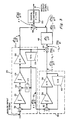
- the intended implementation of the high order sigma delta analog-to-digital converter network is in a sampled data switched capacitor third order circuit in accordance with the discrete-time domain functional block diagram of Figure 4.
- a design objective with oversampled modulators is the scaling of analog signal levels to be on the order of the reference voltage. Therefore, a discrete time version is shown in Figure 4 to indicate that such version is possible for the converter network in which the present invention is embodied.
- each of integrators 22, 24 and 36 is shown as a one cycle delay register 60 preceded by an adder (or summing) unit 62.
- Digital double differentiator 46 is shown as a pair of cascaded differentiators 78, each comprising a delay register 80 followed by a digital subtractor 82.
- An amplifier 84 having a gain coefficient k 1a is situated in second order modulator 20 at the input to an integrator 22 and following a summing unit 32.
- An amplifier 86 with a gain coefficient k 1b couples the output of integrator 22 to the input of an integrator 24 through a summing unit 34.
- Another amplifier 88 with a gain coefficient 2k 1a k 1b is situated in a feedback loop of second order modulator 20 between the output of a digital-to-analog converter 28 and a negative input to summing unit 34, while a second feedback loop in modulator 20 is provided by coupling the output of converter 28 to a negative input of summing unit 32.
- An amplifier 92 of gain j1 couples the output of integrator 24 to a subtractive summing unit 42 in first order modulator 30, while an amplifier 90 having a gain coefficient k2 is situated at the input of integrator 36 after summing unit 42.
- a digital multiplier 74 having a multiplier coefficient g1 couples the output of analog-to-digital converter 38 of first order modulator 30 to digital subtractor 44, while digital-to-analog converter 40 couples the output of analog-to-digital converter 38 to subtractive summing unit 42.
- the output of analog-to-digital converter 26 of second order modulator 20 is connected through a delay register 76 to the negative input of digital subtractor 44 and to digital adder 48.
- a dashed line 9 designates the separation between digital circuitry 21 and analog circuitry 19.
- amplifiers 84 and 86 in second order modulator 20 and amplifier 90 in first order modulator 30 each have a gain coefficient of 1/2, and digital multiplier 74 has a multiplier coefficient of 4.
- This implementation requires only one-bit A/D and D/A converters.
- a switched capacitor implementation of the network of Figure 5 is shown in Figure 6 and employs a single-ended signal flow and stray-free integrators.
- integrators are described, for example, in R. Gregorian, "Analog MOS Integrated Circuits for Signal Processing" previously cited, at pages 277-280, incorporated herein by reference.
- integrator 22 is embodied as a high gain differential amplifier (op amp) 100 provided with a feedback capacitor 102 and a switched input capacitor 104.
- a switch S1 is provided for switching a capacitor 104 between the analog input signal and the feedback loop of modulator 20.
- a switch S2 is provided for switching the output voltage of capacitor 104 between the two inputs of differential amplifier 100.
- integrator 24 is embodied as a high gain differential amplifier (op amp) 110 provided with a feedback capacitor 112 and a pair of switched input capacitors 114 and 103.
- a switch S 4 is provided for switching capacitor 114 between the analog output signal from differential amplifier 100 and ground, while a switch S 9 is provided for switching capacitor 103 between the feedback loop of modulator 20 and ground.
- a switch S4 is provided for switching the output voltages of capacitors 114 and 103 between the two inputs of differential amplifier 110.
- a comparator 116 operated at a sample rate ⁇ 1 converts the analog output signal from differential amplifier 110 into a binary output signal. This binary output signal is stored by a latch 118 and applied via a delay register 76 to the negative input of digital subtractor 44 and to digital adder 48.
- the output signal from latch 118 also controls a switch S5 for switching the feedback loop between a positive reference voltage +V ref and a negative reference voltage -V ref depending on whether the polarity of the latched output signal from comparator 116 is
- integrator 36 is embodied as a high gain differential amplifier (op amp) 120 provided with a feedback capacitor 122 and a switched input capacitor 124.
- a switch S6 is provided for switching capacitor 124 between the analog output signal from differential amplifier 110 and the feedback loop of modulator 30.
- a switch S7 is provided for switching the output voltage of capacitor 124 between the two inputs of differential amplifier 120.
- a comparator 126 operated at a sampling rate ⁇ 1 converts the analog output signal from differential amplifier 120 into a binary output signal. This binary output signal is stored by a latch 128, multiplied by four by multiplier 74, and applied to digital subtractor 44.
- the output signal of latch 128 also controls a switch S8 for switching the feedback loop between a positive reference voltage +V ref and a negative reference voltage -V ref depending on whether polarity of the latched output signal from comparator 126 is positive or negative.
- the digital difference signal produced by digital subtractor 44 is differentiated twice by digital double differentiator 46 and the resultant differentiated signal is applied to digital adder 48.
- the switches which may be implemented by metal-oxide-semiconductor switching devices, as known in the art, are all shown in a common phase ⁇ 1.
- Switches S1-S4, S6, S7 and S9 are analog switches controlled by clock phase signals ⁇ 1, ⁇ 2 which are derived from an oscillator or clock circuit (not shown).
- the clock signals are nonoverlapped and 180° out of phase.
- capacitor 104 charges to the amplitude of the analog input signal while capacitor 114 charges to the output voltage of amp 100 and capacitor 124 charges to the output voltage of op amp 110. At the same time capacitor 103 is totally discharged.
- Switches S5 and S8, both shown connected to a positive reference voltage, are controlled by the output signal of latch 118 and 128, respectively.
- switch S5 or S8, respectively is connected to a positive reference voltage, and is connected to a negative reference voltage when the latched value of the output signal of comparator 116 or 126, respectively, is low.
- D/A converter 28 supplies a selected reference voltage through switch S5, shown as being of positive polarity, which is added to the voltage on capacitor 104 and applied to the inverting input of amplifier 100. This input signal is integrated up in capacitor 102 until reoccurrence of clock phase ⁇ 1.
- the previous (i.e., phase ⁇ 1) output voltage of amplifier 100, stored in capacitor 114, plus the reference voltage from switch S5 which is now stored on capacitor 103, are supplied to the inverting input of amplifier 110, and the previous (i.e., phase ⁇ 1) output voltage of amplifier 110, stored on capacitor 124, is supplied to the inverting input of amplifier 120.
- Each of amplifiers 100, 110 and 120 thus performs an integration of the input voltage supplied to its respective inverting input terminal until phase ⁇ 1 again occurs.
- the switch S5 is connected to the positive reference +V ref , while if the signal is negative, switch S5 is connected to the negative reference -V ref .
- the signal at the comparator input is determined by an integration of a difference between the voltage developed on capacitors 103 and 114.
- the voltage on the output of integrator 22 is an integration of the difference between the input signal and either the positive or negative references depending on the position of switch S5.
- the output signal of integrator 22 can also be viewed as the difference between the analog input signal and the digital representation of the analog input signal.
- Integrator 22 acts as a noninverting integrator for the analog input signal, and as an inverting integrator for one-bit D/A converter 28 controlled by comparator 116.
- the output signal of integrator 22 changes every phase ⁇ 2 by an amount (V in - V D/A1 )k 1a , where V D/A1 is the output voltage of D/A converter 28 while, during phase ⁇ 1, the output signal of integrator 22 remains held at the value established on the previous phase ⁇ 2.
- Integrator 36 operates in a similar manner, except that its input signal is the output signal of integrator 24 less the output signal of D/A converter 40; that is, the integrator 36 output signal changes every phase ⁇ 2 by an amount (V2 - V D/A2 )k2, where V2 is the output voltage of integrator 36 and is held on phase ⁇ 1, and V D/A2 is the output voltage of D/A converter 40.
- integrator 24 is slightly different from that of integrators 22 and 36 in that it uses separate capacitors 114 and 103 for its two input signals. This is necessary since different capacitor ratios are required for the two input signals to integrator 24. Specifically, the output signal of integrator 22 should be integrated with ratio k 1b while the output signal of D/A converter 28 needs to be integrated with ratio -2k 1a k 1b , and therefore a combination of a noninverting and inverting switched capacitor integrator is employed as integrator 24. Through use of superposition, multiple input signals are accommodated by common connection at switch S4 adjacent to the summing junction of op amp 110.
- switch S4 can be shared, though individual switches S3 and S9 are needed for connection to the two input signals.
- the output signal of integrator 24 changes every phase ⁇ 2 by an amount k 1b V2 - 2k 1a k 1b V D/A2 and is held during phase ⁇ 1.
- k 1a 1/2
- the two input capacitors 114 and 103 have the same value and a single capacitor may be used instead, as with integrators 22 and 36.
- the circuit of Figure 6 is quite tolerant of capacitor mismatch errors.
- the remaining switched capacitor integrator 24 uses separate switched capacitors 114 and 103 to take the difference of its two input signals; however, matching errors here are negligible when referred to the input.
- the other remaining summation or difference operations are implemented digitally and are also error free.
- the only component mismatch related error is the departure of the product k 1a k 1b from equaling 1/j1g1.
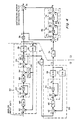
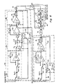
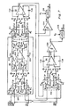
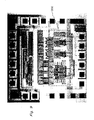
- the power and area reduction technique of this invention has been applied to a prototype third order oversampled modulator shown in Figures 7, 9 and 10.
- the first integrator 22 employs a larger op amp 222, larger respective feedback capacitors 223 and 224, respectively, and input (sampling) capacitors 201 and 202, respectively, and larger metal-oxide-semiconductor (MOS) switches S12, S13, S14 and S15 than are used in the second and third integrators 24 and 36, respectively, in order to minimize kT/C noise in the first integrator.
- MOS metal-oxide-semiconductor
- Op amp 222 of first integrator 22 is of larger power rating than op amps 232 and 242 of subsequent integrators 24 and 36, respectively, to more rapidly charge and discharge capacitors 223, 224, 201 and 202.
- a chopper 200 can be used in first integrator 22, connected as shown in Figure 7, to reduce noise in the first integrator. Since a chopper is not needed in the subsequent integrators, the chip areas utilized by these later integrators can be further reduced.
- Each of op amps 222, 232 and 242 employs balanced inputs and balanced outputs.
- first integrator 22 the capacitance values of feedback capacitors 223 and 224 were 8pF and the capacitance values of input capacitors 201 and 202 were 4pF, while in the second and third integrators, the capacitance values of the feedback capacitors were 1pF and of the input capacitors were 1/2pF.
- the large op amp 222 dissipated 18.8 mW of power while the small op amps 232 and 242 each dissipated 4.8 mW of power.
- the area occupied by the large integrator 22 was 0.39 mm2 and the areas occupied by the small integrators 24 and 36 were 0.18 mm2 each. These areas also did not scale by a factor of eight due to the requirement for matching to the layout pitch of the larger integrator.
- the relative sizes of integrators 22, 24 and 36 on the chip can be seen in the modulator portion 300 of the plot shown in Figure 9 and shown in greater detail in Figure 10.
- the following table provides a comparison of the reduced power/area version-of the A/D converter network of the invention to a conventional version of the network in terms of power and area savings. This table indicates that significant improvement in both power dissipation and area is obtained in this particular implementation. It is contemplated that even greater benefit will result with use of higher order modulators.
- the modulator components i.e., the integrators, the analog-to-digital converters, and the digital-to-analog converters
- the third order sigma delta analog-to-digital converter network of this invention can be implemented with a differential signal path using integrators with fully differential outputs for improved rejection of power supply noise.
- the invention is not limited to use of a digital decimation filter and any signal processing circuit capable of eliminating differential noise components can be employed.
Landscapes
- Engineering & Computer Science (AREA)
- Theoretical Computer Science (AREA)
- Compression, Expansion, Code Conversion, And Decoders (AREA)
- Analogue/Digital Conversion (AREA)
Applications Claiming Priority (2)
| Application Number | Priority Date | Filing Date | Title |
|---|---|---|---|
| US505382 | 1983-06-17 | ||
| US07/505,382 US5065157A (en) | 1990-04-06 | 1990-04-06 | High order sigma delta oversampled analog-to-digital converter integrated circuit network with minimal power dissipation and chip area requirements |
Publications (2)
| Publication Number | Publication Date |
|---|---|
| EP0450947A2 true EP0450947A2 (fr) | 1991-10-09 |
| EP0450947A3 EP0450947A3 (en) | 1992-03-04 |
Family
ID=24010094
Family Applications (1)
| Application Number | Title | Priority Date | Filing Date |
|---|---|---|---|
| EP19910302955 Pending EP0450947A3 (en) | 1990-04-06 | 1991-04-04 | Analog-to-digital converter |
Country Status (6)
| Country | Link |
|---|---|
| US (1) | US5065157A (fr) |
| EP (1) | EP0450947A3 (fr) |
| JP (1) | JPH04225624A (fr) |
| KR (1) | KR100221914B1 (fr) |
| CN (1) | CN1030026C (fr) |
| IL (1) | IL95256A (fr) |
Cited By (6)
| Publication number | Priority date | Publication date | Assignee | Title |
|---|---|---|---|---|
| EP0559944A1 (fr) * | 1992-03-12 | 1993-09-15 | Siemens Aktiengesellschaft | Modulateur du type sigma-delta |
| EP0660530A1 (fr) * | 1993-12-21 | 1995-06-28 | Advanced Micro Devices, Inc. | Modulateur sigma-delta en cascade |
| US5621675A (en) * | 1994-11-02 | 1997-04-15 | Advanced Micro Devices, Inc. | Digital decimation and compensation filter system |
| US5646621A (en) * | 1994-11-02 | 1997-07-08 | Advanced Micro Devices, Inc. | Delta-sigma ADC with multi-stage decimation filter and gain compensation filter |
| US5648779A (en) * | 1994-12-09 | 1997-07-15 | Advanced Micro Devices, Inc. | Sigma-delta modulator having reduced delay from input to output |
| US5751615A (en) * | 1995-11-14 | 1998-05-12 | Advanced Micro Devices, Inc. | Implementation of a digital decimation filter and method |
Families Citing this family (44)
| Publication number | Priority date | Publication date | Assignee | Title |
|---|---|---|---|---|
| KR100219021B1 (ko) * | 1990-04-06 | 1999-09-01 | 제이 엘. 차스킨, 버나드 스나이더, 아더엠. 킹 | 성분 감도가 낮은 오버샘플된 3차 시그마 델타 아날로그-디지탈 변환기 네트워크 |
| US5187482A (en) * | 1992-03-02 | 1993-02-16 | General Electric Company | Delta sigma analog-to-digital converter with increased dynamic range |
| US5203335A (en) * | 1992-03-02 | 1993-04-20 | General Electric Company | Phased array ultrasonic beam forming using oversampled A/D converters |
| US5181033A (en) * | 1992-03-02 | 1993-01-19 | General Electric Company | Digital filter for filtering and decimating delta sigma modulator output signals |
| US5241310A (en) * | 1992-03-02 | 1993-08-31 | General Electric Company | Wide dynamic range delta sigma analog-to-digital converter with precise gain tracking |
| US5283578A (en) * | 1992-11-16 | 1994-02-01 | General Electric Company | Multistage bandpass Δ Σ modulators and analog-to-digital converters |
| US5446460A (en) | 1993-11-03 | 1995-08-29 | Advanced Micro Devices, Inc. | Fourth-order cascaded sigma-delta modulator |
| US5732002A (en) * | 1995-05-23 | 1998-03-24 | Analog Devices, Inc. | Multi-rate IIR decimation and interpolation filters |
| US5654711A (en) * | 1995-06-07 | 1997-08-05 | Asahi Kasei Microsystems Ltd. | Analog-to-digital converter with local feedback |
| US5565867A (en) * | 1995-08-23 | 1996-10-15 | General Electric Company | Distributed analog to digital converter with optical links |
| US5732004A (en) * | 1995-11-14 | 1998-03-24 | Advanced Micro Devices, Inc. | DSP architecture for a FIR-type filter and method |
| US5818374A (en) * | 1996-05-08 | 1998-10-06 | Telefonaktiebolaget Lm Ericsson | Switched current delta-sigma modulator |
| US5682160A (en) * | 1996-05-20 | 1997-10-28 | Ribner; David Byrd | High-order delta sigma analog-to-digital converter with unit-delay integrators |
| US5682161A (en) * | 1996-05-20 | 1997-10-28 | General Electric Company | High-order delta sigma modulator |
| US5760723A (en) * | 1996-06-10 | 1998-06-02 | General Electric Company | Delta-sigma analog-to-digital converter including charge coupled devices |
| US5754131A (en) * | 1996-07-01 | 1998-05-19 | General Electric Company | Low power delta sigma converter |
| US5757300A (en) * | 1996-10-22 | 1998-05-26 | General Electric Company | Feed-forward bandpass delta-sigma converter with tunable center frequency |
| US5790063A (en) * | 1996-12-16 | 1998-08-04 | Motorola, Inc. | Analog-to-digital converter on CMOS with MOS capacitor |
| US6147551A (en) * | 1998-01-05 | 2000-11-14 | Motorola, Inc. | Switched capacitor circuit and method for reducing sampling noise |
| US6963626B1 (en) | 1998-10-02 | 2005-11-08 | The Board Of Trustees Of The Leland Stanford Junior University | Noise-reducing arrangement and method for signal processing |
| US6255974B1 (en) * | 1999-01-08 | 2001-07-03 | Mitsubishi Electric And Electronics Usa, Inc | Programmable dynamic range sigma delta A/D converter |
| US6201835B1 (en) | 1999-03-05 | 2001-03-13 | Burr-Brown Corporation | Frequency-shaped pseudo-random chopper stabilization circuit and method for delta-sigma modulator |
| US6359576B1 (en) * | 1999-10-01 | 2002-03-19 | Linear Technology Corporation | Apparatus and methods for performing RMS-to-DC conversion with bipolar input signal range |
| WO2003051374A2 (fr) * | 2001-12-17 | 2003-06-26 | New York State Office Of Mental Health | SEQUESTRATION DE Aβ DANS LA REGION PERIPHERIQUE EN L'ABSENCE D'AGENTS IMMUNOMODULATEURS COMME APPROCHE THERAPEUTIQUE POUR LE TRAITEMENT OU LA PREVENTION DES MALADIES LIEES A LA BETA-AMYLOIDE |
| JP3785361B2 (ja) * | 2001-12-25 | 2006-06-14 | 株式会社ルネサステクノロジ | Δςモジュレータ、a/dコンバータおよびd/aコンバータ |
| JP3904111B2 (ja) * | 2002-06-04 | 2007-04-11 | ソニー株式会社 | 固体撮像装置及びその信号処理方法 |
| CN1305127C (zh) * | 2003-09-12 | 2007-03-14 | 清华大学 | 用去耦合电容实现集成电路供电网络噪声优化的快速方法 |
| JP2005117618A (ja) * | 2003-09-19 | 2005-04-28 | Sharp Corp | 集積回路及び光ピックアップ装置 |
| US6940436B2 (en) * | 2003-10-31 | 2005-09-06 | Texas Instruments Incorporated | Analog-to-digital conversion system with second order noise shaping and a single amplifier |
| US6864818B1 (en) | 2003-12-09 | 2005-03-08 | Texas Instruments Incorporated | Programmable bandpass analog to digital converter based on error feedback architecture |
| US7199743B2 (en) * | 2004-12-29 | 2007-04-03 | Intel Corporation | Cyclic digital to analog converter |
| JP4589275B2 (ja) * | 2006-07-27 | 2010-12-01 | パナソニック株式会社 | デルタシグマ変調型da変換装置 |
| US9135962B2 (en) | 2007-06-15 | 2015-09-15 | Micron Technology, Inc. | Comparators for delta-sigma modulators |
| US7817073B2 (en) * | 2007-06-15 | 2010-10-19 | Micron Technology, Inc. | Integrators for delta-sigma modulators |
| US7782237B2 (en) * | 2008-06-13 | 2010-08-24 | The Board Of Trustees Of The Leland Stanford Junior University | Semiconductor sensor circuit arrangement |
| CN101350623B (zh) * | 2008-09-16 | 2011-08-10 | 华为技术有限公司 | 一种调制器电路及实现方法 |
| KR101703358B1 (ko) * | 2010-12-21 | 2017-02-06 | 엘지이노텍 주식회사 | 노이즈 저감 아날로그 디지털 컨버터 |
| CN103329442B (zh) * | 2011-01-21 | 2016-10-26 | 联发科技(新加坡)私人有限公司 | 连续时间积分三角模数转换器 |
| CN102082553B (zh) * | 2011-02-28 | 2014-04-09 | 中国科学院等离子体物理研究所 | 差分输入的积分器 |
| CN106130556B (zh) * | 2016-07-12 | 2019-10-01 | 昆明物理研究所 | 一种两步式增量模拟-数字转换器及两步式转换方法 |
| JP7139588B2 (ja) * | 2017-09-22 | 2022-09-21 | カシオ計算機株式会社 | 変換装置、電子楽器、情報処理装置、変換方法及びプログラム |
| CN113312585B (zh) * | 2021-05-26 | 2022-06-10 | 广东电网有限责任公司 | 高阶控制策略参数调节的高频噪声功率增益在线跟踪方法 |
| CN117240291A (zh) * | 2023-08-28 | 2023-12-15 | 芯海科技(深圳)股份有限公司 | 一种模数转换电路、控制方法、芯片及电子设备 |
| CN117914309B (zh) * | 2024-03-19 | 2024-05-31 | 成都中微达信科技有限公司 | 分子时钟、分子时钟频率控制方法和电子设备 |
Family Cites Families (5)
| Publication number | Priority date | Publication date | Assignee | Title |
|---|---|---|---|---|
| CA1144653A (fr) * | 1980-08-27 | 1983-04-12 | Adrian Worsman | Codeur-decodeur |
| US4704600A (en) * | 1985-02-04 | 1987-11-03 | Nippon Telegraph And Telephone Corporation | Oversampling converter |
| US4876542A (en) * | 1988-01-25 | 1989-10-24 | Motorola, Inc. | Multiple output oversampling A/D converter with each output containing data and noise |
| JPH01204528A (ja) * | 1988-02-10 | 1989-08-17 | Fujitsu Ltd | A/d変換器 |
| US4896156A (en) * | 1988-10-03 | 1990-01-23 | General Electric Company | Switched-capacitance coupling networks for differential-input amplifiers, not requiring balanced input signals |
-
1990
- 1990-04-06 US US07/505,382 patent/US5065157A/en not_active Expired - Lifetime
- 1990-08-01 IL IL95256A patent/IL95256A/xx active IP Right Grant
- 1990-08-31 CN CN90107496A patent/CN1030026C/zh not_active Expired - Lifetime
-
1991
- 1991-03-22 JP JP3081120A patent/JPH04225624A/ja active Pending
- 1991-04-03 KR KR1019910005340A patent/KR100221914B1/ko not_active Expired - Lifetime
- 1991-04-04 EP EP19910302955 patent/EP0450947A3/en active Pending
Cited By (7)
| Publication number | Priority date | Publication date | Assignee | Title |
|---|---|---|---|---|
| EP0559944A1 (fr) * | 1992-03-12 | 1993-09-15 | Siemens Aktiengesellschaft | Modulateur du type sigma-delta |
| US5298900A (en) * | 1992-03-12 | 1994-03-29 | Siemens Aktiengesellschaft | Sigma-delta modulator |
| EP0660530A1 (fr) * | 1993-12-21 | 1995-06-28 | Advanced Micro Devices, Inc. | Modulateur sigma-delta en cascade |
| US5621675A (en) * | 1994-11-02 | 1997-04-15 | Advanced Micro Devices, Inc. | Digital decimation and compensation filter system |
| US5646621A (en) * | 1994-11-02 | 1997-07-08 | Advanced Micro Devices, Inc. | Delta-sigma ADC with multi-stage decimation filter and gain compensation filter |
| US5648779A (en) * | 1994-12-09 | 1997-07-15 | Advanced Micro Devices, Inc. | Sigma-delta modulator having reduced delay from input to output |
| US5751615A (en) * | 1995-11-14 | 1998-05-12 | Advanced Micro Devices, Inc. | Implementation of a digital decimation filter and method |
Also Published As
| Publication number | Publication date |
|---|---|
| CN1055454A (zh) | 1991-10-16 |
| KR910019348A (ko) | 1991-11-30 |
| IL95256A (en) | 1993-06-10 |
| IL95256A0 (en) | 1991-06-30 |
| KR100221914B1 (ko) | 1999-09-15 |
| CN1030026C (zh) | 1995-10-11 |
| US5065157A (en) | 1991-11-12 |
| JPH04225624A (ja) | 1992-08-14 |
| EP0450947A3 (en) | 1992-03-04 |
Similar Documents
| Publication | Publication Date | Title |
|---|---|---|
| US5065157A (en) | High order sigma delta oversampled analog-to-digital converter integrated circuit network with minimal power dissipation and chip area requirements | |
| US5148166A (en) | Third order sigma delta oversampled analog-to-digital converter network with low component sensitivity | |
| US5148167A (en) | Sigma-delta oversampled analog-to-digital converter network with chopper stabilization | |
| US7084797B2 (en) | Delta sigma modulating apparatus | |
| US5103229A (en) | Plural-order sigma-delta analog-to-digital converters using both single-bit and multiple-bit quantization | |
| US5311181A (en) | Sigma delta modulator | |
| US5682161A (en) | High-order delta sigma modulator | |
| US5084702A (en) | Plural-order sigma-delta analog-to-digital converter using both single-bit and multiple-bit quantizers | |
| US5055843A (en) | Sigma delta modulator with distributed prefiltering and feedback | |
| JP3240145B2 (ja) | デルタ・シグマ変調器 | |
| US5030954A (en) | Double rate oversampled interpolative modulators for analog-to-digital conversion | |
| US5949361A (en) | Multi-stage delta sigma modulator with one or more high order sections | |
| US6111531A (en) | Parallel architecture for a bandpass sigma-delta modulator | |
| EP0796525B1 (fr) | Modulateur sigma-delta avec retard reduit de l'entree a la sortie | |
| US5414424A (en) | Fourth-order cascaded sigma-delta modulator | |
| US6147631A (en) | Input sampling structure for delta-sigma modulator | |
| JPWO1996041422A1 (ja) | デルタ・シグマ変調器 | |
| Chen et al. | Analysis and design of sigma-delta ADCs for automotive control systems | |
| CN111865309A (zh) | 增量式模拟数字转换器 | |
| US10469098B2 (en) | Non-switched capacitor circuits for delta-sigma ADCs | |
| Okamoto et al. | A stable high-order delta-sigma modulator with an FIR spectrum distributor | |
| JP2001156642A (ja) | マルチビット−デルタシグマad変換器 | |
| IL98080A (en) | Sigma-delta oversampled analog-to-digital converter network with chopper stabilization | |
| Pelgrom | Time-Discrete Σ Δ Modulation | |
| IL95523A (en) | Sigma Delta integrated circuit network Third-degree over-sampling with low component sensitivity |
Legal Events
| Date | Code | Title | Description |
|---|---|---|---|
| PUAI | Public reference made under article 153(3) epc to a published international application that has entered the european phase |
Free format text: ORIGINAL CODE: 0009012 |
|
| AK | Designated contracting states |
Kind code of ref document: A2 Designated state(s): DE FR GB IT NL |
|
| PUAL | Search report despatched |
Free format text: ORIGINAL CODE: 0009013 |
|
| AK | Designated contracting states |
Kind code of ref document: A3 Designated state(s): DE FR GB IT NL |
|
| 18D | Application deemed to be withdrawn |
Effective date: 19920905 |
|
| D18D | Application deemed to be withdrawn (deleted) | ||
| STAA | Information on the status of an ep patent application or granted ep patent |
Free format text: STATUS: THE APPLICATION IS DEEMED TO BE WITHDRAWN |
|
| R18D | Application deemed to be withdrawn (corrected) |
Effective date: 19920905 |