EP0451674B1 - Borne à implanter - Google Patents
Borne à implanter Download PDFInfo
- Publication number
- EP0451674B1 EP0451674B1 EP91105213A EP91105213A EP0451674B1 EP 0451674 B1 EP0451674 B1 EP 0451674B1 EP 91105213 A EP91105213 A EP 91105213A EP 91105213 A EP91105213 A EP 91105213A EP 0451674 B1 EP0451674 B1 EP 0451674B1
- Authority
- EP
- European Patent Office
- Prior art keywords
- contact
- length
- press
- shank
- shank part
- Prior art date
- Legal status (The legal status is an assumption and is not a legal conclusion. Google has not performed a legal analysis and makes no representation as to the accuracy of the status listed.)
- Expired - Lifetime
Links
- 230000007704 transition Effects 0.000 claims description 5
- 239000000463 material Substances 0.000 claims description 2
- 238000000034 method Methods 0.000 description 1
- 239000007787 solid Substances 0.000 description 1
Images
Classifications
-
- H—ELECTRICITY
- H01—ELECTRIC ELEMENTS
- H01R—ELECTRICALLY-CONDUCTIVE CONNECTIONS; STRUCTURAL ASSOCIATIONS OF A PLURALITY OF MUTUALLY-INSULATED ELECTRICAL CONNECTING ELEMENTS; COUPLING DEVICES; CURRENT COLLECTORS
- H01R12/00—Structural associations of a plurality of mutually-insulated electrical connecting elements, specially adapted for printed circuits, e.g. printed circuit boards [PCB], flat or ribbon cables, or like generally planar structures, e.g. terminal strips, terminal blocks; Coupling devices specially adapted for printed circuits, flat or ribbon cables, or like generally planar structures; Terminals specially adapted for contact with, or insertion into, printed circuits, flat or ribbon cables, or like generally planar structures
- H01R12/50—Fixed connections
- H01R12/51—Fixed connections for rigid printed circuits or like structures
- H01R12/55—Fixed connections for rigid printed circuits or like structures characterised by the terminals
- H01R12/58—Fixed connections for rigid printed circuits or like structures characterised by the terminals terminals for insertion into holes
- H01R12/585—Terminals having a press fit or a compliant portion and a shank passing through a hole in the printed circuit board
Definitions
- Press-in contacts of this type are known, for example, from EP-A-0 234 235 and are used to produce solderless electrical connections which, as so-called press-in connections, can correspond to DIN 41 611, Part 5 (September 1984).
- the generic press-in contact corresponds to the EE design, because the press-in area of its shaft part which forms the actual press-in pin is designed to be elastic, that is to say the forces required for the press-in connection are applied by deformation of the elastic shaft part and the printed circuit board receiving the press-in contact. - See section 3.2.2 of DIN 41 611, part 5 -.
- the contact in the circuit board hole is improved compared to press-in contacts with a solid press-in pin or shaft part, for example in accordance with the EM design in accordance with DIN 41 611, part 5, section 3.2.1.
- the object of the invention is to improve the contacting of the known press-in contacts in the pressed-in state and to counteract excessive deformation of the legs delimiting the slot opening.
- the shaft part tapers from the middle of its length to the connecting pin approximately linearly to half its maximum width and the remaining length of the shaft part between the connecting pin and the end of the slot opening facing it is a fraction of half the length of the shaft part corresponds.
- the ratio of the remaining length of the shaft part to half the length of the shaft part is in a range between 0.45: 1 and 0.35: 1, preferably 0.4: 1.
- this new design of the press-in contact can be achieved in that the slot opening in the shaft part is extended accordingly in the direction of the connecting pin while maintaining its spatial shape.
- the distance of the slot opening in the shaft part from the press-in shoulder can be 0.34 mm amount, while the length of the slot opening corresponds to 2.78 mm.
- the remaining length of the shaft part thus remains 0.88 mm, which is a ratio of 0.44: 1 to half the length of the shaft part.
- press-in contacts according to the invention are particularly well suited for use with printed circuit boards with a nominal thickness of 3.2 mm, but that they can also be used without problems in connection with printed circuit boards of smaller nominal thickness, for example 2.4 and 1. 6 mm.
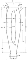
- a connecting pin 5 is connected to the shaft part 2, a part of which is also only hinted at.
- the press-in shoulder 3 serves the purpose of limiting the press-in path of the shaft part 2 into a plated-through hole 6 of a printed circuit board 7, the upper side of the printed circuit board 7 and the hole 6 being only indicated by dash-dotted lines.
- the shaft part 2 is provided with a slot opening 8, the ends 9 and 10 of which each have a parabolic design, while their center has a constriction 11.
- the end 9 of the slot opening facing the contact spring or the contact pin 4 almost reaches the press-in shoulder 3 and is therefore only a short distance 12 from the latter.
- the other end 10 of the slot opening 8 is at a certain distance 13 from the transition between the shaft part 2 and the connecting pin 5. It can also be seen in the drawing that the shaft part 2 extends from the middle of its length to the connecting pin 5, that is to say above the length range 14 tapers away from its maximum width 15 to a dimension 16 which corresponds to approximately half of the maximum width 15.
- the length 17 of the slot opening 8 is limited between the two distances 12 and 13.
- the middle shaft part 2 of the press-in contact 1 has legs 18 and 19 on each side of the slot opening 8.
- the total length 20 of the middle shaft part 2 corresponds to the length 17 of the slot opening 8 plus the two distances 12 and 13.
- the slot opening 8 has a position in the middle shaft part 2 such that the remaining length of the shaft part 2 corresponding to the distance 13 is in a ratio to the length range 14 corresponding to half the length thereof, which is between 0.45: 1 and 0.35: 1 and is preferably about 0.4: 1.
- the remaining length of the shaft part 2 corresponding to the distance 13 is in a ratio of, for example, 0.314: 1 to the length 17 of the slot opening 8, and the distance 12 to the length 17 of the slot opening 8 is in a ratio of, for example, 0. 12: 1.
- the press-in contact 1 is designed according to the drawing so that the length 17 of the slot opening 8 is in a ratio of about 0.7: 1 to the total length 20 of the central shaft part 2.
- the width of the slot opening 8 in the region of the constriction 11 to the greatest width thereof in the region of the parabolic ends 9 and 10 has a ratio of approximately 0.73: 1 to 0.74: 1.
Landscapes
- Coupling Device And Connection With Printed Circuit (AREA)
- Multi-Conductor Connections (AREA)
Claims (4)
- Borne à implanter (1) destinée à être implantée dans un perçage (6) à contact intérieur d'une plaque à circuits (7), comprenant:- une lamelle de contact ou une tige de contact (4),- une partie de tronc (2) médiane qui s'y raccorde, et- une tige de raccordement (5) qui forme un prolongement de la partie de tronc médiane,dans laquelle la lamelle ou la tige de contact (4) présente, dans la région de transition vers la partie de tronc (2), un épaulement d'implantation (3) qui limite le trajet d'implantation du contact (1) dans la plaque de circuit (7), et
dans laquelle la partie de tronc (2) est dotée d'une ouverture traversante en forme de fente (8), délimitée latéralement par des ailes (18, 19), ouverte sur la totalité de sa longueur à l'intérieur du plan normal de la partie de tronc médiane (2), et située dans l'épaisseur normale du matériau de la partie de tronc (2),
et où l'extrémité de l'ouverture en forme de fente (8) orientée vers la lamelle ou la tige de contact (4) s'étend pratiquement jusqu'à l'épaulement d'implantation (3), tandis que son autre extrémité est située à une certaine distance de la transition entre la partie de tronc (2) et la tige de raccordement (5),
caractérisée en ce que l'ouverture en forme de fente (8) est réalisée de telle manière que dans la condition non implantée, elle présente une forme parabolique à ses extrémités (9, 10), tandis qu'elle présente en son milieu un rétrécissement (11) formé par un élargissement des ailes (18, 19),
et en ce que l'ouverture en forme de fente (8) va en se rétrécissant à partir des extrémités terminales paraboliques, de façon incurvée et jusque dans la région du rétrécissement (11). - Contact à implanter selon la revendication 1, caractérisé en ce que la partie de tronc (2) va en se rétrécissant depuis la moitié de sa longueur et jusqu'à la tige de raccordement (5) approximativement de façon linéaire et jusqu'à la moitié de sa largeur maximum,
et en ce que la longueur restante de la partie de tronc entre la tige de raccordement et l'extrémité de l'ouverture en fente orientée vers ladite tige correspond à une fraction de la demi-longueur de la partie de tronc. - Borne à implanter selon les revendications 1 et 2, caractérisée en ce que le rapport entre la longueur restante (13) de la partie de tronc (2) et la demi-longueur (14) de la partie de tronc (2) est situé dans la plage entre 0,45:1 et 0,35:1, de préférence égal à environ 0,4:1.
- Borne à implanter selon la revendication 1, caractérisée en ce que l'ouverture en fente s'étend de façon rectiligne et parallèle dans la région du rétrécissement.
Applications Claiming Priority (2)
| Application Number | Priority Date | Filing Date | Title |
|---|---|---|---|
| DE9004090U | 1990-04-09 | ||
| DE9004090U DE9004090U1 (de) | 1990-04-09 | 1990-04-09 | Einpreßkontakt |
Publications (2)
| Publication Number | Publication Date |
|---|---|
| EP0451674A1 EP0451674A1 (fr) | 1991-10-16 |
| EP0451674B1 true EP0451674B1 (fr) | 1995-06-28 |
Family
ID=6852746
Family Applications (1)
| Application Number | Title | Priority Date | Filing Date |
|---|---|---|---|
| EP91105213A Expired - Lifetime EP0451674B1 (fr) | 1990-04-09 | 1991-04-02 | Borne à implanter |
Country Status (2)
| Country | Link |
|---|---|
| EP (1) | EP0451674B1 (fr) |
| DE (2) | DE9004090U1 (fr) |
Cited By (3)
| Publication number | Priority date | Publication date | Assignee | Title |
|---|---|---|---|---|
| DE10229331A1 (de) * | 2002-06-29 | 2004-01-29 | Conti Temic Microelectronic Gmbh | Einpresskontakt |
| US7008272B2 (en) | 2003-10-23 | 2006-03-07 | Trw Automotive U.S. Llc | Electrical contact |
| DE202011004165U1 (de) | 2011-03-19 | 2011-07-20 | Elco Europe Gmbh | Einpresskontakt |
Families Citing this family (9)
| Publication number | Priority date | Publication date | Assignee | Title |
|---|---|---|---|---|
| US5823830A (en) * | 1995-02-24 | 1998-10-20 | Wurster; Woody | Tailess compliant contact |
| DE19726759A1 (de) * | 1997-06-24 | 1999-01-07 | Elco Europ Gmbh | Einpreßkontakt |
| DE19831672B4 (de) * | 1998-07-15 | 2005-05-12 | Ludger Sorig | Einpreßkontakt |
| FR2985864B1 (fr) * | 2012-01-12 | 2014-02-07 | Loupot | Contact pour emmanchement en force |
| DE202016105003U1 (de) | 2016-09-09 | 2016-09-23 | Andreas Veigel | Steckverbinder |
| DE102019112697A1 (de) | 2019-05-15 | 2020-11-19 | Andreas Veigel | Drahtverbindungselement |
| DE202020105848U1 (de) | 2020-10-13 | 2022-02-10 | Andreas Veigel | Drahtverbindungselement |
| DE202020107455U1 (de) | 2020-12-22 | 2022-03-29 | Andreas Veigel | Leiterplattensteckverbinder |
| DE202022102403U1 (de) | 2022-05-03 | 2022-05-23 | Andreas Veigel | Steckverbinder |
Citations (1)
| Publication number | Priority date | Publication date | Assignee | Title |
|---|---|---|---|---|
| WO1990003050A1 (fr) * | 1988-09-01 | 1990-03-22 | Amp Incorporated | Broche flexible avec adaptabilite amelioree |
Family Cites Families (2)
| Publication number | Priority date | Publication date | Assignee | Title |
|---|---|---|---|---|
| US4606589A (en) * | 1984-01-12 | 1986-08-19 | H & V Services | Compliant pin |
| GB2186124A (en) * | 1986-01-30 | 1987-08-05 | Plessey Co Plc | Contact pin |
-
1990
- 1990-04-09 DE DE9004090U patent/DE9004090U1/de not_active Expired - Lifetime
-
1991
- 1991-04-02 DE DE59105821T patent/DE59105821D1/de not_active Expired - Fee Related
- 1991-04-02 EP EP91105213A patent/EP0451674B1/fr not_active Expired - Lifetime
Patent Citations (1)
| Publication number | Priority date | Publication date | Assignee | Title |
|---|---|---|---|---|
| WO1990003050A1 (fr) * | 1988-09-01 | 1990-03-22 | Amp Incorporated | Broche flexible avec adaptabilite amelioree |
Cited By (4)
| Publication number | Priority date | Publication date | Assignee | Title |
|---|---|---|---|---|
| DE10229331A1 (de) * | 2002-06-29 | 2004-01-29 | Conti Temic Microelectronic Gmbh | Einpresskontakt |
| DE10229331B4 (de) * | 2002-06-29 | 2016-03-24 | Conti Temic Microelectronic Gmbh | Einpresskontakt |
| US7008272B2 (en) | 2003-10-23 | 2006-03-07 | Trw Automotive U.S. Llc | Electrical contact |
| DE202011004165U1 (de) | 2011-03-19 | 2011-07-20 | Elco Europe Gmbh | Einpresskontakt |
Also Published As
| Publication number | Publication date |
|---|---|
| EP0451674A1 (fr) | 1991-10-16 |
| DE9004090U1 (de) | 1990-06-13 |
| DE59105821D1 (de) | 1995-08-03 |
Similar Documents
| Publication | Publication Date | Title |
|---|---|---|
| EP0887883B1 (fr) | Borne à implanter | |
| DE69525623T2 (de) | Elektrischer Verbinder mit verbessertem Verriegelungssystem | |
| DE1122603B (de) | Steckerbuchse | |
| DE2435461C2 (de) | Elektrischer Kontaktstift | |
| EP0793313A2 (fr) | Connecteur d'insérage à angle droit à insérer en force dans les trous d'un circuit imprimé | |
| DE2414640B2 (de) | Elektrischer Verbinder mit einer metallischen Anschlußklemme | |
| EP0451674B1 (fr) | Borne à implanter | |
| DE7146935U (de) | Steckdoseneinheit zur Aufnahme elektronischer Bestandteile | |
| DE1465477A1 (de) | Kontakt mit abgebogenem Ansatzstueck | |
| DE102004019360A1 (de) | Isolierdraht-Anschlusskontaktelement | |
| DE102009019699B4 (de) | Anschlussklemme für Leiterplatten | |
| EP0416306A1 (fr) | Elément de contact éléctrique | |
| DE2344045C2 (de) | Lüsterklemme | |
| DE69913397T2 (de) | Schneidklemme | |
| DE69802579T2 (de) | Elastisch befestigtes elektrisches Kontaktelement | |
| EP0226907A2 (fr) | Relais | |
| DE69903231T2 (de) | Kontaktteil für Verbindungsbuchse und Verbinder mit einem solchen Kontaktteil | |
| DE4400702A1 (de) | Einstückige Steckervorrichtung | |
| DE1816073C3 (de) | Zur Verbindung mit einer Schaltungsplatine vorgesehenes elektrisches Bauelement | |
| EP0980116A1 (fr) | Borne femelle, prise ayant une telle borne et méthode pour la fabrication d'une borne | |
| DE3030906C2 (de) | Umschaltsteckvorrichtung mit einem Brückenstecker | |
| DE2551970A1 (de) | Elektrische flachsteckbuchsen | |
| DE2713728A1 (de) | Kontaktelement fuer steckverbindungen | |
| EP0793302A1 (fr) | Ressort de contact plat ayant plusieurs lamelles | |
| DE602004011607T2 (de) | Blattfederanschlussklemme mit reduzierter Einsteckkraft |
Legal Events
| Date | Code | Title | Description |
|---|---|---|---|
| PUAI | Public reference made under article 153(3) epc to a published international application that has entered the european phase |
Free format text: ORIGINAL CODE: 0009012 |
|
| 17P | Request for examination filed |
Effective date: 19910422 |
|
| AK | Designated contracting states |
Kind code of ref document: A1 Designated state(s): BE CH DE FR GB IT LI NL |
|
| RAP3 | Party data changed (applicant data changed or rights of an application transferred) |
Owner name: ELCO EUROPE GMBH |
|
| 17Q | First examination report despatched |
Effective date: 19940201 |
|
| GRAA | (expected) grant |
Free format text: ORIGINAL CODE: 0009210 |
|
| AK | Designated contracting states |
Kind code of ref document: B1 Designated state(s): BE CH DE FR GB IT LI NL |
|
| PG25 | Lapsed in a contracting state [announced via postgrant information from national office to epo] |
Ref country code: NL Free format text: LAPSE BECAUSE OF FAILURE TO SUBMIT A TRANSLATION OF THE DESCRIPTION OR TO PAY THE FEE WITHIN THE PRESCRIBED TIME-LIMIT Effective date: 19950628 Ref country code: GB Effective date: 19950628 |
|
| REF | Corresponds to: |
Ref document number: 59105821 Country of ref document: DE Date of ref document: 19950803 |
|
| ITF | It: translation for a ep patent filed | ||
| ET | Fr: translation filed | ||
| NLV1 | Nl: lapsed or annulled due to failure to fulfill the requirements of art. 29p and 29m of the patents act | ||
| GBV | Gb: ep patent (uk) treated as always having been void in accordance with gb section 77(7)/1977 [no translation filed] |
Effective date: 19950628 |
|
| REG | Reference to a national code |
Ref country code: CH Ref legal event code: NV Representative=s name: ULRICH UND BRIGITTE BALLMER PATENTANWAELTE |
|
| PLBE | No opposition filed within time limit |
Free format text: ORIGINAL CODE: 0009261 |
|
| STAA | Information on the status of an ep patent application or granted ep patent |
Free format text: STATUS: NO OPPOSITION FILED WITHIN TIME LIMIT |
|
| 26N | No opposition filed | ||
| PGFP | Annual fee paid to national office [announced via postgrant information from national office to epo] |
Ref country code: BE Payment date: 20080522 Year of fee payment: 18 Ref country code: IT Payment date: 20080426 Year of fee payment: 18 |
|
| PGFP | Annual fee paid to national office [announced via postgrant information from national office to epo] |
Ref country code: FR Payment date: 20090414 Year of fee payment: 19 Ref country code: DE Payment date: 20090422 Year of fee payment: 19 |
|
| PGFP | Annual fee paid to national office [announced via postgrant information from national office to epo] |
Ref country code: CH Payment date: 20090417 Year of fee payment: 19 |
|
| BERE | Be: lapsed |
Owner name: *ELCO EUROPE G.M.B.H. Effective date: 20090430 |
|
| PG25 | Lapsed in a contracting state [announced via postgrant information from national office to epo] |
Ref country code: BE Free format text: LAPSE BECAUSE OF NON-PAYMENT OF DUE FEES Effective date: 20090430 |
|
| REG | Reference to a national code |
Ref country code: CH Ref legal event code: PL |
|
| REG | Reference to a national code |
Ref country code: FR Ref legal event code: ST Effective date: 20101230 |
|
| PG25 | Lapsed in a contracting state [announced via postgrant information from national office to epo] |
Ref country code: LI Free format text: LAPSE BECAUSE OF NON-PAYMENT OF DUE FEES Effective date: 20100430 Ref country code: DE Free format text: LAPSE BECAUSE OF NON-PAYMENT OF DUE FEES Effective date: 20101103 Ref country code: CH Free format text: LAPSE BECAUSE OF NON-PAYMENT OF DUE FEES Effective date: 20100430 |
|
| PG25 | Lapsed in a contracting state [announced via postgrant information from national office to epo] |
Ref country code: IT Free format text: LAPSE BECAUSE OF NON-PAYMENT OF DUE FEES Effective date: 20090402 |
|
| PG25 | Lapsed in a contracting state [announced via postgrant information from national office to epo] |
Ref country code: FR Free format text: LAPSE BECAUSE OF NON-PAYMENT OF DUE FEES Effective date: 20100430 |