EP0451754A1 - Digitaler autoadaptiver Entzerrer - Google Patents
Digitaler autoadaptiver Entzerrer Download PDFInfo
- Publication number
- EP0451754A1 EP0451754A1 EP91105515A EP91105515A EP0451754A1 EP 0451754 A1 EP0451754 A1 EP 0451754A1 EP 91105515 A EP91105515 A EP 91105515A EP 91105515 A EP91105515 A EP 91105515A EP 0451754 A1 EP0451754 A1 EP 0451754A1
- Authority
- EP
- European Patent Office
- Prior art keywords
- bits
- output
- signal
- type
- coefficient
- Prior art date
- Legal status (The legal status is an assumption and is not a legal conclusion. Google has not performed a legal analysis and makes no representation as to the accuracy of the status listed.)
- Granted
Links
- 230000005540 biological transmission Effects 0.000 claims description 23
- 238000013139 quantization Methods 0.000 claims description 17
- 230000006870 function Effects 0.000 claims description 6
- 238000000429 assembly Methods 0.000 claims description 3
- 230000033764 rhythmic process Effects 0.000 claims 2
- 238000007792 addition Methods 0.000 description 7
- 238000010586 diagram Methods 0.000 description 3
- 238000011002 quantification Methods 0.000 description 3
- 230000009471 action Effects 0.000 description 2
- 230000000295 complement effect Effects 0.000 description 2
- 230000000694 effects Effects 0.000 description 2
- 238000001914 filtration Methods 0.000 description 2
- 230000009467 reduction Effects 0.000 description 2
- 230000004044 response Effects 0.000 description 2
- 238000011144 upstream manufacturing Methods 0.000 description 2
- 241001080024 Telles Species 0.000 description 1
- 230000006978 adaptation Effects 0.000 description 1
- 238000004364 calculation method Methods 0.000 description 1
- 238000009434 installation Methods 0.000 description 1
- 238000000034 method Methods 0.000 description 1
- 230000008569 process Effects 0.000 description 1
- 229910052710 silicon Inorganic materials 0.000 description 1
- 239000010703 silicon Substances 0.000 description 1
Images
Classifications
-
- H—ELECTRICITY
- H04—ELECTRIC COMMUNICATION TECHNIQUE
- H04L—TRANSMISSION OF DIGITAL INFORMATION, e.g. TELEGRAPHIC COMMUNICATION
- H04L25/00—Baseband systems
- H04L25/02—Details ; arrangements for supplying electrical power along data transmission lines
- H04L25/03—Shaping networks in transmitter or receiver, e.g. adaptive shaping networks
- H04L25/03006—Arrangements for removing intersymbol interference
- H04L25/03012—Arrangements for removing intersymbol interference operating in the time domain
- H04L25/03019—Arrangements for removing intersymbol interference operating in the time domain adaptive, i.e. capable of adjustment during data reception
- H04L25/03057—Arrangements for removing intersymbol interference operating in the time domain adaptive, i.e. capable of adjustment during data reception with a recursive structure
Definitions
- the invention relates to a digital self-adjusting equalizer intended to correct the distortions introduced by a transmission channel on the digital signals which it transmits, when the bit rate is high, for example of the order of a few megabits / second.
- Such a self-adjusting equalizer which can be used to effect echo cancellation with various types of transmission links of different lengths, is for example associated with a link of relatively short length, less than one kilometer, comprising a pair of twisted wires which serves a private telecommunications facility.
- equalizers are associated with high-performance transmission links, these equalizers are preferably chosen to be self-adaptive, when the knowledge of the transmission characteristics of the links concerned is likely to be imprecise.
- analog-to-digital converters and digital multipliers are sub-assemblies which require a relatively large surface area of silicon, which is disadvantageous when they are provided in integrated circuits. They are therefore quite expensive and are not suitable for general purpose digital transmission links intended for example to serve digital terminals in a multi-service switch type installation in the private telecommunications sector, where cost is an important factor.
- the invention therefore proposes a digital self-adapting equalizer, rapid and integrable at a reduced cost, which is intended to correct the distortions introduced by a transmission link on a digital signal in code with "n" levels which it ensures the transmission.
- This equalizer intended for signals received for which the number "n" of levels is equal to or greater than three, is intended to be connected at the output of a link by a correcting device receiving on the one hand the signal transmitted by the link and on the other hand a symbol correction signal from a filter.
- the output signal from said correcting device is binarily transcoded by a quantization device, in order to be processed by the filter, the latter is able to take account of binary transcodings, temporarily stored, which have been carried out for "i" successive symbols of the received signal, in order to establish the correction signal to be applied, as a function of at least one initial adapter coefficient, to each symbol arriving via the transmission link.
- said equalizer comprises a correcting device constituted by an analog subtractor receiving on the one hand the signal coming from the transmission link and on the other hand the symbol correction signal supplied by a converter, of digital-analog type, placed at the output of the filter which is provided with a binary transcoding buffer memory and which comprises corrective logic constituted using binary logic gates associating the transcoding bits contained in the buffer memory for "i" successive symbols of the received signal with "iq" bits corresponding to "i" adapter coefficients successively obtained from each other, from an initial coefficient by an updating device as a function of an error finding result supplied in binary form for each successive symbol by the quantification device.
- a correcting device constituted by an analog subtractor receiving on the one hand the signal coming from the transmission link and on the other hand the symbol correction signal supplied by a converter, of digital-analog type, placed at the output of the filter which is provided with a binary transcoding buffer memory and which comprises corrective logic constituted using binary logic gates associating the transcoding bits contained in the buffer memory for "i" successive symbols
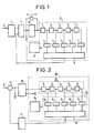
- Figure 1 shows a block diagram of a known self-adjusting equalizer.
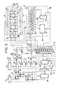
- Figure 2 shows a block diagram of a self-adjusting equalizer according to the invention.
- Figure 3 shows a detailed diagram of the equalizer shown in Figure 2.
- the self-adapting equalizer of conventional type, presented in FIG. 1 essentially comprises an analog / digital converter 1 receiving the digital signals transmitted by a transmission link 2, in order to reconstitute digital signals usable by the circuits located downstream.
- Link 2 connects for example a telephone terminal to a coupler of the multiservice switch which serves it.
- the converter 1 must be very fast to allow the reconstruction of the symbols of a received signal and it must therefore work at a frequency at least equal to the transmission frequency of these symbols, it is generally composed of comparators in parallel whose number is a function of the desired resolution, this therefore results in the occupation of a relatively large support surface in the case of an integrated VLSI circuit.
- a digital filter 0 is positioned downstream of the converter 1, it is for example of the type comprising a set of flip-flops 3, or of registers, arranged in series and forming a buffer memory, as well as a corrective logic constituted using multipliers 4 associated with a summator 5 and with an updating device 6.
- each flip-flop 3 is connected to an individual multiplier 4, also receiving a multiplier coefficient coming from the updating device 6.
- the signals obtained from the multipliers 4 are transmitted in parallel to a first summator 5 which supplies the output signal from the filter, the latter possibly being looped back, if the filter is of the infinite impulse response type.
- the loopback is carried out by means of a second summator 7, of digital type, serving as a correcting device, which is positioned between the converter 1 and the first of series of flip-flops 3.
- This second adder 7 makes it possible to correct the signals received before their transmission to an output S1 for exploitation and to the filter for interpretation.
- a quantization device 8 is placed between the output of the second adder 7 and the first of series of flip-flops 3, it makes it possible to introduce non-linearity in the signals transmitted to this series of registers 3.
- a subtractor 9 connected on the one hand to the input and on the other hand to the output of the quantization device 8 makes it possible to know the error introduced.
- the input of the auto-adaptive equalizer according to the invention which is presented in FIG. 2, is constituted by a correcting device produced in the form of an analog subtractor 17, for example using operational amplifiers and resistances.
- This subtractor 17 is connected at the output of the transmission link 2, possibly via a conventional automatic gain correction circuit, not shown here.
- this subtractor 17 is fast and compact, it receives the digital signals transmitted by the link 2 on a first of its inputs, its output attacks an input of a quantization device 18, formed using comparators, which also receives by other inputs reference signals corresponding to the different possible theoretical levels of the expected digital signals, for example three, four or five levels.
- the code for transmitting the signals received from the transmission link 2 is for example an AMI code and the expected theoretical levels are therefore +1, -1 and 0.
- a digital filter 10 is connected to the first output of the quantization device 18, it comprises a set of flip-flops 3, of type D, forming a buffer memory 13 for the data supplied by the quantization device for "i" successive binary transcodings of symbol of the signal received.
- the digital filter 10 also includes a corrective logic 12, this is in particular composed of one or more logic modules 14 each corresponding to a binary multiplier device, as well as a summator 15, it is associated with a device update 16.
- the modules 14 are individually connected each at the output of a rocker 3.
- the summer 15 receives in parallel the output signals coming simultaneously from the modules 14, the sum signal which it supplies in digital form, is converted into analog form by a converter 11 which is placed at the output of the filter 10.
- the analog subtractor 17 which receives the degraded digital signals arriving from the transmission link 2 on a first input also receives, as correction signal, the signal supplied by the converter 11, of digital-analog type; it itself provides corrected signals at an output S2.
- Each module 14 replaces a multiplier 4 of the prior art, since under the conditions chosen, simple additions or subtractions replace the multiplications usually carried out.
- the filter coefficients are individually supplied by the updating device 16 to the operating logic 12 in order to be used there.
- the latter is for example produced using resistors according to a conventional arrangement making it possible to obtain high speed at low cost.
- the analog signal obtained is applied to the subtractor 17 and makes it possible to correct the degraded digital signals which are received by this subtractor from the transmission link 2.
- FIG. 3 presents an exemplary embodiment of a self-adapting equalizer according to the invention where, in particular, a reduction in the number of components is obtained at the level of the filter and consequently a reduction in surface area, in the case of a VLSI circuit.
- the proposed self-adaptive equalizer which is of the recursive type with decision in the loop, is not linear and therefore does not amplify the noise.
- this self-adapting equalizer receives the degraded digital signals coming from the transmission link 2 via a conventional automatic gain correction circuit, here referenced 20, which brings for example the level of the signals received between zero and five volts.
- This gain correction circuit 20 drives a first input of an analog subtractor 17, a second input of which receives the correction signal supplied by a converter 11, of digital-analog type, as indicated in connection with FIG. 2.
- the subtractor 17 is produced for example around an operational amplifier 21 whose non-inverting input is connected to the common point of a divider bridge with resistors 22, 23 in series between the ground and the output of the gain correction circuit 20.
- the inverting input of the operational amplifier 21 receives the correction signal which is applied to it via a resistor 24, either directly by the output of the converter 11, or through an inverting amplifier 26, the choice of one or the other of the channels being effected, according to the direction of the correction to be made and by means of a switch 27, controlled in a manner which will be discussed later.
- An equalized signal appears at the output of the operational amplifier 21, it is simultaneously applied in feedback to the inverting input of this operational amplifier 21, via a resistor 28, at the input of a phase locked loop 31 for recovering the clock contained in the signals received from the transmission link 2 and at the input of the quantization device 18.
- the latter comprises a set of five comparators 32 to 36, produced using as many operational amplifiers identically connected to the output of the operational amplifier 21, each by its respective non-inverting input, and each individually connected to a different positive reference potential by its inverting input, the five potentials here being distributed equally from zero up to five volts.
- the transmission code of the signals received from the transmission link 2 being assumed at three levels corresponding respectively to the ternary values -1, 0 and +1, it suffices for a first arrangement associating two comparators, here comparators 33 and 35, connected each by its output at a different input of a gate 37, of the exclusive OR type, and an inverter 38, inserted between the comparator 33 and the gate 37, to quantify in amplitude the signals appearing at the output of the operational amplifier 21, the reference potentials of the comparators 33 and 35 being respectively assumed one of 1.25 volts and the other of 3.75 volts.
- the quantization in sign for the ternary values +1 and -1 is carried out simply by taking account of the binary signal present at the output of the inverter 38.
- a complementary arrangement makes it possible to establish the sign of the error introduced by the quantization in amplitude defined above.
- This complementary arrangement associates the three comparators 32, 34 and 36 mentioned above, whose respective reference potentials are here 0, 2.5 and 5 volts, a plurality of gates 39 to 42 and two inverters 43, 44 to the amplifiers. 33, 35 and to the reverser 38 of the first arrangement.
- Gate 40 of type OR, here provides a binary indication of value one, called a positive error, when the signal at the output of the operational amplifier 21 is greater than the reference potential associated with the signal of ternary value which has been quantified. .
- the gate 40 provides a binary indication of zero value, called negative error, when the signal at the output of the operational amplifier 21 is lower than the reference potential associated with the signal of ternary value which has been quantified.
- the gate 40 has its two inputs at binary level 0 under the respective action of the gate 39, of the AND type and of the gate 41, of the OR type, the gate 39 being connected by a first input to the comparator 32 output corresponding to the ternary value threshold -1, that is to say 0 volts, and by a second input at the output of comparator 33, via the inverter 38.
- This comparator 33 indicates the position of the received signal with respect to the median threshold of 1.25 volts which allows the taking into account of a received signal with a ternary value -1 or 0, depending on whether this signal is between 0 and 1, 25 volts or between 1.25 and 2.5 volts.
- the door 40 which is connected at the outlet of the doors 39 and 41 is connected by the latter, with a part at the output of comparator 36 controlling the position of the received signal with respect to the 5 volt threshold corresponding to the ternary value 1, on the other hand at the output of a gate 42, of ET type.
- the latter has three inputs respectively connected at the output of the comparator 34, at the output of the comparator 35, via an inverter 43, and at the output of the comparator 36, via another inverter 44.
- the signals appearing at the output of the gate 37 and the inverter 38 which respectively translate the absolute value of the amplitude of the received signal as restored and its sign, are applied to the assembly 13 grouping the flip-flops 3 of the self-adjusting equalizer according to the invention.
- the buffer memory 13 comprises a number "i" within five stages and it is composed of two sub-assemblies each comprising a series of five flip-flops 3.
- a first of these subsets is connected at the output of gate 37 and receives on an input of a flip-flop 3A located upstream of its series, the symbol amplitude bits successively defined from the received signal.
- the second of these subsets is connected at the output of the inverter 38 and receives, on an input of a rocker 3B located upstream of its series, the successive bits which correspond to the sign of said symbols.
- all the flip-flops of the buffer memory 13 which are of identical constitution have their clock inputs which are controlled by the phase locked loop 31, the latter providing them with clock signals bit CK from the received signal.
- the self-matching function of the equalizer according to the invention is obtained by applying an individual adapter coefficient to the signal appearing at the output of each of the five stages, each coefficient being capable of varying according to variations affecting the symbols of the received signal.
- the "i" flip-flops 3A to 3Y of the first subset have their respective outputs connected to as many individual inputs of a multiplexer 45 addressed by a counter 46 receiving a clock signal iCK produced by the loop at phase locking 31 from the clock signal CK, the signal iCK having a frequency which is "i" times that of the signal CK.
- the multiplexer 45 is connected to the corrective logic 12 which here comprises a single logic module 14 which is used “i" times consecutively for the supply of each symbol correction signal.
- This module 14 is composed of "q-1" doors 47, of the AND type and of a door 50, of the exclusive OR type, an adder 15 is functionally associated with it.
- the output signal from the multiplexer 45 drives a first input from each of the parallel doors 47.
- each door 47 is connected to one of the different outputs of a register 48, of the first input-first output type, with "i" stages and "q" parallel outputs.
- the register 48 is able to contain, in each of its "i” stages, the "q-1" binary values defining a coefficient at a given instant, as well as an additional value corresponding to the sign to which this coefficient must be assigned.
- These values are initially supplied to the register 48 by an external means, for example by an external processor, via a link 49.
- the door 50 is mounted parallel to the doors 47, it receives on a first input the sign signal supplied by the register 48 and on a second input that which provides a multiplexer 51 connected to the outputs of flip-flops 3B to 3Z of the second subset in which temporarily store the characteristic sign bits obtained from the quantization device 18, by transcoding, for successive symbols of the received signal.
- This multiplexer 51 and the multiplexer 45 are addressed by the counter 46 so as to simultaneously supply, at each clock time iCK, the absolute amplitude value bit and the sign bit obtained during the binary transcoding of a symbol.
- a second group of "q" inputs of the unit 52 are looped back, via the locking register 53, to its "q" outputs to ensure the addition of any combination of bits appearing at the level of the first group of inputs of this unit 52 with the combination obtained at the output, during the previous addition.
- the unit 52 and the register 53 are controlled by the clock signal iCK, while the latch register 54, whose inputs are in parallel with those of the register 53, is controlled by the clock signal CK.
- This register provides a sign bit for the control of the switch 27 contained in the analog subtractor 17.
- the converter 11 simultaneously receives "q-1" bits from the register 54 in output of which it is connected with the switch 27 and it produces a signal, in the form of an electric voltage, which is applied for action to the subtractor 17, at an inverting input of the operational amplifier 26 and via resistance 30.
- a permanent update of the coefficients of the equalizer is ensured by means of an updating device 16 capable of receiving the "q" bits for defining a coefficient initially supplied by the equalizer, via the link 49, and the two output bits respectively supplied by the gate 40 and by the multiplexer 51.
- the "q-1" bits corresponding to the absolute value of a coefficient and the bit relating to the sign assigned to this coefficient are individually transmitted by the link 49 to a logic module 59 identical to the module 14 and therefore composed of "q- 1 "doors 58, of type ET, each connected by a first input to an individual wire of the connection 49, these doors receiving in parallel, on a second input, the amplitude bit supplied by the multiplexer 45 at each time d iCK clock.
- the sign bit emanating from the link 49 is transmitted to an input of a gate 58, of the exclusive OR type, a second input of which is connected at the output of another gate 56, also of the exclusive OR type, which receives on the one hand the sign bit supplied by the gate 40 for each transcoding carried out from an incoming symbol, on the other hand the sign bit supplied by the multiplexer 51.
- the "q" bits supplied at each clock time iCK by the doors 55 and by the door 58 are applied to a first group of inputs of an adder 57 whose "q" outputs are connected to the inputs of the register 48 whose "q" outputs are on the one hand, as we saw it, connected to the inputs of doors 47 and 50 of the assembly looped back to a second group of inputs, so as to add the "q" bits received on the first group of inputs to each iCK clock time with the bits obtained at the output of the adder 57 at the previous iCK clock time.
- the updating device 16 receives a bit relating to the sign of the error affecting any symbol transcoded by the quantizing device 18, at the clock rate CK, and modifies the direction of the correction to be made by modifying the sign bit supplied by this device for updating the adder 57, if necessary.
- the register 48 provides the "q" bits of a coefficient at the rate of the clock iCK to the module 14 of the equalizer so that each of the "i" additions made by the adder circuit 52 can take into account the calculation obtained from a combination of two transcoding bits corresponding to a symbol and from one of the corresponding "i" updated coefficients.
Landscapes
- Engineering & Computer Science (AREA)
- Power Engineering (AREA)
- Computer Networks & Wireless Communication (AREA)
- Signal Processing (AREA)
- Cable Transmission Systems, Equalization Of Radio And Reduction Of Echo (AREA)
- Filters That Use Time-Delay Elements (AREA)
- Dc Digital Transmission (AREA)
- Analogue/Digital Conversion (AREA)
- Road Signs Or Road Markings (AREA)
- Bidirectional Digital Transmission (AREA)
Applications Claiming Priority (2)
| Application Number | Priority Date | Filing Date | Title |
|---|---|---|---|
| FR9004589A FR2660819B1 (fr) | 1990-04-10 | 1990-04-10 | Egaliseur autoadaptatif numerique. |
| FR9004589 | 1990-04-10 |
Publications (2)
| Publication Number | Publication Date |
|---|---|
| EP0451754A1 true EP0451754A1 (de) | 1991-10-16 |
| EP0451754B1 EP0451754B1 (de) | 1995-03-29 |
Family
ID=9395615
Family Applications (1)
| Application Number | Title | Priority Date | Filing Date |
|---|---|---|---|
| EP91105515A Expired - Lifetime EP0451754B1 (de) | 1990-04-10 | 1991-04-08 | Digitaler autoadaptiver Entzerrer |
Country Status (6)
| Country | Link |
|---|---|
| EP (1) | EP0451754B1 (de) |
| AT (1) | ATE120592T1 (de) |
| DE (1) | DE69108433T2 (de) |
| DK (1) | DK0451754T3 (de) |
| ES (1) | ES2071147T3 (de) |
| FR (1) | FR2660819B1 (de) |
Cited By (2)
| Publication number | Priority date | Publication date | Assignee | Title |
|---|---|---|---|---|
| ES2048092A2 (es) * | 1992-02-14 | 1994-03-01 | Alcatel Standard Electrica | Ecualizador automatico digital asincrono para transmision de datos por cable. |
| WO1999014912A1 (en) * | 1997-09-18 | 1999-03-25 | Level One Communications, Inc. | Method and apparatus for modified baud rate sampling |
Citations (2)
| Publication number | Priority date | Publication date | Assignee | Title |
|---|---|---|---|---|
| US4186384A (en) * | 1975-06-24 | 1980-01-29 | Honeywell Inc. | Signal bias remover apparatus |
| EP0022558A1 (de) * | 1979-07-13 | 1981-01-21 | Siemens Aktiengesellschaft | Schaltungsanordnung zur Amplitudenregelung bei einer automatischen adaptiven, zeitlichen Entzerrung der Nachschwinger eines mindestens dreipegeligen Basisbandsignals |
-
1990
- 1990-04-10 FR FR9004589A patent/FR2660819B1/fr not_active Expired - Fee Related
-
1991
- 1991-04-08 EP EP91105515A patent/EP0451754B1/de not_active Expired - Lifetime
- 1991-04-08 ES ES91105515T patent/ES2071147T3/es not_active Expired - Lifetime
- 1991-04-08 DE DE69108433T patent/DE69108433T2/de not_active Expired - Fee Related
- 1991-04-08 DK DK91105515.0T patent/DK0451754T3/da active
- 1991-04-08 AT AT91105515T patent/ATE120592T1/de not_active IP Right Cessation
Patent Citations (2)
| Publication number | Priority date | Publication date | Assignee | Title |
|---|---|---|---|---|
| US4186384A (en) * | 1975-06-24 | 1980-01-29 | Honeywell Inc. | Signal bias remover apparatus |
| EP0022558A1 (de) * | 1979-07-13 | 1981-01-21 | Siemens Aktiengesellschaft | Schaltungsanordnung zur Amplitudenregelung bei einer automatischen adaptiven, zeitlichen Entzerrung der Nachschwinger eines mindestens dreipegeligen Basisbandsignals |
Cited By (3)
| Publication number | Priority date | Publication date | Assignee | Title |
|---|---|---|---|---|
| ES2048092A2 (es) * | 1992-02-14 | 1994-03-01 | Alcatel Standard Electrica | Ecualizador automatico digital asincrono para transmision de datos por cable. |
| WO1999014912A1 (en) * | 1997-09-18 | 1999-03-25 | Level One Communications, Inc. | Method and apparatus for modified baud rate sampling |
| US6061396A (en) * | 1997-09-18 | 2000-05-09 | Level One Communications, Inc. | Method and apparatus for modified baud rate sampling |
Also Published As
| Publication number | Publication date |
|---|---|
| FR2660819A1 (fr) | 1991-10-11 |
| DK0451754T3 (da) | 1995-07-31 |
| DE69108433D1 (de) | 1995-05-04 |
| ATE120592T1 (de) | 1995-04-15 |
| DE69108433T2 (de) | 1995-07-27 |
| EP0451754B1 (de) | 1995-03-29 |
| ES2071147T3 (es) | 1995-06-16 |
| FR2660819B1 (fr) | 1993-05-07 |
Similar Documents
| Publication | Publication Date | Title |
|---|---|---|
| EP0107233B1 (de) | Basisbandsignal-Echoentzerrer | |
| EP0096936B1 (de) | Verfahren zur Verkürzung der Konvergenzzeit eines Echokompensators sowie Vorrichtung zur Durchführung dieses Verfahrens | |
| FR2471094A1 (fr) | Circuit interpolateur augmentant le debit de mots d'un signal numerique du type utilise dans les systemes telephoniques a commutation numerique et joncteur de ligne equipe d'un tel circuit | |
| EP0808538B1 (de) | Verfahren, modul und vorrichtung zum empfang digitaler signale mit iterativer arbeitsweise | |
| FR2652692A1 (fr) | Procede et appareil pour obtenir le gain de codage integral pour des signaux numeriques codes. | |
| FR2602938A1 (fr) | Ensemble d'abonne pour telephonie numerique sans fil; modem et dispositifs divers (synthetiseur de frequence...) pour cet ensemble | |
| EP0106406A1 (de) | Selbstadaptiver Entzerrer für Basisband-Datensignal | |
| EP0178720A1 (de) | Einrichtung zum Empfang von digitalen Daten mit einer adaptiven Taktrückgewinnungsschaltung | |
| FR2524742A1 (fr) | Procede de transmission de donnees en duplex sur un circuit telephonique commute et modem correspondant | |
| EP0013343A1 (de) | Verfahren und Vorrichtung zur Auffindung einer Pseudo-Zufallsfolge von 0 Grad- und 180 Grad-Phasenänderungen der Trägerwelle in einem Datenempfänger | |
| FR2468258A1 (fr) | Circuit de correction des bruits de phase pour un systeme de transmission | |
| FR2471093A1 (fr) | Circuit et procede de commande de gain pour signal numerique du type utilise dans les systemes telephoniques a commutation numerique et joncteur de ligne equipe d'un tel circuit | |
| EP0011341A1 (de) | Differenz-Pulscodemodulation verwendendes Übertragungssystem | |
| EP0078581A1 (de) | Differentialpulscode-Modulationssystem mit adaptiver Prädiktion | |
| CH640678A5 (fr) | Procede et installation de transmission simultanee d'une onde basse frequence et d'un signal numerique mic. | |
| EP0451754B1 (de) | Digitaler autoadaptiver Entzerrer | |
| EP0275790B1 (de) | Datenendgerät zur Übertragung über einer analoge Zweiwegleitung mit an den Empfangstakt gekoppelter Echokompensation | |
| EP0857385B1 (de) | Verfahren und vorrichtung zur digital-analogen nachrichtenübertragung | |
| EP0318105B1 (de) | Analoge Schaltung für Basisband-Modem | |
| FR2546693A1 (fr) | Annuleur d'echo a filtre numerique adaptatif pour systeme de transmission | |
| EP0028551A1 (de) | Speichernder Komparator zur Regenerierung digitaler elektrischer Signale und digitales Übertragungssystem, das einen solchen Komparator verwendet | |
| EP0030194B1 (de) | Prediktorstufe für ein System zur Kompression des Datenflusses | |
| FR2485304A1 (fr) | Dispositif de traitement audiofrequence de ligne d'abonne | |
| CA2196209C (fr) | Procede de compensation des differences en temps de propagation de groupe entre les filtres analogiques d'un emetteur et ceux d'un recepteur de signaux en quadrature de phase, dispositif de compensation et systeme de transmission correspondants | |
| WO1998052329A1 (fr) | Dispositif d'egalisation et de decodage pour un canal de transmission numerique selectif en frequence |
Legal Events
| Date | Code | Title | Description |
|---|---|---|---|
| PUAI | Public reference made under article 153(3) epc to a published international application that has entered the european phase |
Free format text: ORIGINAL CODE: 0009012 |
|
| AK | Designated contracting states |
Kind code of ref document: A1 Designated state(s): AT BE CH DE DK ES FR GB IT LI NL SE |
|
| 17P | Request for examination filed |
Effective date: 19911218 |
|
| 17Q | First examination report despatched |
Effective date: 19940216 |
|
| GRAA | (expected) grant |
Free format text: ORIGINAL CODE: 0009210 |
|
| AK | Designated contracting states |
Kind code of ref document: B1 Designated state(s): AT BE CH DE DK ES FR GB IT LI NL SE |
|
| REF | Corresponds to: |
Ref document number: 120592 Country of ref document: AT Date of ref document: 19950415 Kind code of ref document: T |
|
| REF | Corresponds to: |
Ref document number: 69108433 Country of ref document: DE Date of ref document: 19950504 |
|
| ITF | It: translation for a ep patent filed | ||
| REG | Reference to a national code |
Ref country code: ES Ref legal event code: FG2A Ref document number: 2071147 Country of ref document: ES Kind code of ref document: T3 |
|
| GBT | Gb: translation of ep patent filed (gb section 77(6)(a)/1977) |
Effective date: 19950606 |
|
| REG | Reference to a national code |
Ref country code: DK Ref legal event code: T3 |
|
| PLBE | No opposition filed within time limit |
Free format text: ORIGINAL CODE: 0009261 |
|
| STAA | Information on the status of an ep patent application or granted ep patent |
Free format text: STATUS: NO OPPOSITION FILED WITHIN TIME LIMIT |
|
| 26N | No opposition filed | ||
| REG | Reference to a national code |
Ref country code: GB Ref legal event code: IF02 |
|
| PGFP | Annual fee paid to national office [announced via postgrant information from national office to epo] |
Ref country code: CH Payment date: 20020319 Year of fee payment: 12 |
|
| PGFP | Annual fee paid to national office [announced via postgrant information from national office to epo] |
Ref country code: SE Payment date: 20020327 Year of fee payment: 12 Ref country code: DK Payment date: 20020327 Year of fee payment: 12 |
|
| PGFP | Annual fee paid to national office [announced via postgrant information from national office to epo] |
Ref country code: NL Payment date: 20020328 Year of fee payment: 12 Ref country code: AT Payment date: 20020328 Year of fee payment: 12 |
|
| PGFP | Annual fee paid to national office [announced via postgrant information from national office to epo] |
Ref country code: GB Payment date: 20020402 Year of fee payment: 12 |
|
| PGFP | Annual fee paid to national office [announced via postgrant information from national office to epo] |
Ref country code: BE Payment date: 20020412 Year of fee payment: 12 |
|
| PGFP | Annual fee paid to national office [announced via postgrant information from national office to epo] |
Ref country code: FR Payment date: 20020416 Year of fee payment: 12 |
|
| PGFP | Annual fee paid to national office [announced via postgrant information from national office to epo] |
Ref country code: ES Payment date: 20020418 Year of fee payment: 12 Ref country code: DE Payment date: 20020418 Year of fee payment: 12 |
|
| PG25 | Lapsed in a contracting state [announced via postgrant information from national office to epo] |
Ref country code: GB Free format text: LAPSE BECAUSE OF NON-PAYMENT OF DUE FEES Effective date: 20030408 Ref country code: AT Free format text: LAPSE BECAUSE OF NON-PAYMENT OF DUE FEES Effective date: 20030408 |
|
| PG25 | Lapsed in a contracting state [announced via postgrant information from national office to epo] |
Ref country code: SE Free format text: LAPSE BECAUSE OF NON-PAYMENT OF DUE FEES Effective date: 20030409 Ref country code: ES Free format text: LAPSE BECAUSE OF NON-PAYMENT OF DUE FEES Effective date: 20030409 |
|
| PG25 | Lapsed in a contracting state [announced via postgrant information from national office to epo] |
Ref country code: LI Free format text: LAPSE BECAUSE OF NON-PAYMENT OF DUE FEES Effective date: 20030430 Ref country code: DK Free format text: LAPSE BECAUSE OF NON-PAYMENT OF DUE FEES Effective date: 20030430 Ref country code: CH Free format text: LAPSE BECAUSE OF NON-PAYMENT OF DUE FEES Effective date: 20030430 Ref country code: BE Free format text: LAPSE BECAUSE OF NON-PAYMENT OF DUE FEES Effective date: 20030430 |
|
| BERE | Be: lapsed |
Owner name: *ALCATEL BUSINESS SYSTEMS Effective date: 20030430 |
|
| PG25 | Lapsed in a contracting state [announced via postgrant information from national office to epo] |
Ref country code: NL Free format text: LAPSE BECAUSE OF NON-PAYMENT OF DUE FEES Effective date: 20031101 Ref country code: DE Free format text: LAPSE BECAUSE OF NON-PAYMENT OF DUE FEES Effective date: 20031101 |
|
| GBPC | Gb: european patent ceased through non-payment of renewal fee |
Effective date: 20030408 |
|
| NLV4 | Nl: lapsed or anulled due to non-payment of the annual fee |
Effective date: 20031101 |
|
| REG | Reference to a national code |
Ref country code: DK Ref legal event code: EBP |
|
| EUG | Se: european patent has lapsed | ||
| REG | Reference to a national code |
Ref country code: CH Ref legal event code: PL |
|
| PG25 | Lapsed in a contracting state [announced via postgrant information from national office to epo] |
Ref country code: FR Free format text: LAPSE BECAUSE OF NON-PAYMENT OF DUE FEES Effective date: 20031231 |
|
| REG | Reference to a national code |
Ref country code: FR Ref legal event code: ST |
|
| REG | Reference to a national code |
Ref country code: ES Ref legal event code: FD2A Effective date: 20030409 |
|
| PG25 | Lapsed in a contracting state [announced via postgrant information from national office to epo] |
Ref country code: IT Free format text: LAPSE BECAUSE OF NON-PAYMENT OF DUE FEES;WARNING: LAPSES OF ITALIAN PATENTS WITH EFFECTIVE DATE BEFORE 2007 MAY HAVE OCCURRED AT ANY TIME BEFORE 2007. THE CORRECT EFFECTIVE DATE MAY BE DIFFERENT FROM THE ONE RECORDED. Effective date: 20050408 |