EP0451767B1 - Stabilisateur de synchronisation de trâme - Google Patents
Stabilisateur de synchronisation de trâme Download PDFInfo
- Publication number
- EP0451767B1 EP0451767B1 EP91105555A EP91105555A EP0451767B1 EP 0451767 B1 EP0451767 B1 EP 0451767B1 EP 91105555 A EP91105555 A EP 91105555A EP 91105555 A EP91105555 A EP 91105555A EP 0451767 B1 EP0451767 B1 EP 0451767B1
- Authority
- EP
- European Patent Office
- Prior art keywords
- pattern
- frame
- counter
- mismatch
- synchronization
- Prior art date
- Legal status (The legal status is an assumption and is not a legal conclusion. Google has not performed a legal analysis and makes no representation as to the accuracy of the status listed.)
- Expired - Lifetime
Links
- 239000003381 stabilizer Substances 0.000 title claims description 56
- 238000001514 detection method Methods 0.000 claims description 20
- 230000000087 stabilizing effect Effects 0.000 claims description 9
- 230000001360 synchronised effect Effects 0.000 description 29
- 230000005540 biological transmission Effects 0.000 description 22
- 238000010276 construction Methods 0.000 description 12
- 238000000034 method Methods 0.000 description 5
- 238000004891 communication Methods 0.000 description 3
- 238000005516 engineering process Methods 0.000 description 2
- 230000008094 contradictory effect Effects 0.000 description 1
- 230000003247 decreasing effect Effects 0.000 description 1
- 238000011144 upstream manufacturing Methods 0.000 description 1
Images




Classifications
-
- H—ELECTRICITY
- H04—ELECTRIC COMMUNICATION TECHNIQUE
- H04J—MULTIPLEX COMMUNICATION
- H04J3/00—Time-division multiplex systems
- H04J3/02—Details
- H04J3/06—Synchronising arrangements
- H04J3/0602—Systems characterised by the synchronising information used
- H04J3/0605—Special codes used as synchronising signal
- H04J3/0608—Detectors therefor, e.g. correlators, state machines
Definitions
- the present invention relates to a frame synchronization stabilizer in accordance with the precharacterizing part of claim 1.
- a frame synchronization stabilizer is known from IEEE Transactions On Communication Technology, Feb. 1968, Vol. 16, No. 1, p. 142-148, HAWKES et al., "Construction and Performance of PCM-Frame Synchronizer with Self-varying Threshold".
- a transmission side transmits a data stream with a frame synchronization pattern for synchronizing the data stream, frame by frame, to a reception side.
- the reception side identifies the synchronization pattern and thereby detects the end of each frame so as to correctly obtain the data.
- a frame synchronization stabilizer is used so as to stabilize the synchronization of frames against a disturbance which may takes place over a transmission line.
- the frame synchronization stabilizer is provided with both a front stabilizing function for preventing it from determining an instantaneous pulse fluctuation due to a bit error over the transmission line as an out-of frame and a rear stabilizing function for preventing it from performing an incorrect synchronization due to an incorrect determination.
- a front stabilizing function for preventing it from determining an instantaneous pulse fluctuation due to a bit error over the transmission line as an out-of frame
- a rear stabilizing function for preventing it from performing an incorrect synchronization due to an incorrect determination.
- the front synchronization stabilizer is provided with a match and mismatch detection circuit for outputting a match pulse or a mismatch pulse depending upon whether a data pattern in an area around the beginning of each received frame, in which area a synchronization pattern should be stored (hereinafter, this area is referred to as a synchronization pattern area), completely matches or mismatches a predetermined synchronization pattern.
- a match and mismatch detection circuit for outputting a match pulse or a mismatch pulse depending upon whether a data pattern in an area around the beginning of each received frame, in which area a synchronization pattern should be stored (hereinafter, this area is referred to as a synchronization pattern area), completely matches or mismatches a predetermined synchronization pattern.
- a reset counter type stabilizer is equipped with a mismatch counter for counting the number of mismatch pulses and for outputting a carry pulse when the counted value exceeds a particular value n (hereinafter, this value n is referred to as the counter size).
- the mismatch counter is reset by the match pulse and by the carry pulse.
- the carry pulse which is outputted from the mismatch counter is outputted as an out-of frame pulse for denoting that an out-of frame is detected.
- the out-of frame pulse is outputted.
- the mismatch pulse is outputted and thereby the mismatch counter is incremented by one.
- the mismatch counter is reset before the counter value becomes the particular value n.
- the out-of frame pulse is not outputted. In other words, even if a disturbance takes place over the transmission line, the out-of frame hardly takes place.
- the mismatch counter continues counting until the counter value becomes the particular value n without being reset and thereby outputs the carry pulse which is the out-of frame pulse. Since the probability of matching data in the synchronization pattern area of each frame inputted with the particular synchronization pattern by chance and thereby for outputting the match pulse is very small, in most cases, the out-of frame pulse is outputted.
- a racing counter type stabilizer is equipped with both a mismatch counter with size n for counting the number of mismatch pulses and for outputting a carry pulse when the count value becomes n and a match counter with size m for counting the number of match pulses and for outputting a carry pulse when the count value becomes a particular value m.
- the mismatch counter and the match counter are reset by the carry pulses being outputted therefrom.
- the carry pulse being outputted from the mismatch counter is outputted as an out-of frame pulse for denoting that an out-of frame is detected.
- the mismatch counter is reset when the number of mismatch pulses becomes the particular value m.
- the threshold value of determining the out-of frame just depends on the size of the mismatch counter.
- the threshold value of determining the out-of frame can be variably set and thereby the degree of freedom of this type stabilizer is higher than that of the other.
- the probability Perr should satisfy the following condition against a particular setting value X (hereinafter, the value X is referred to as the threshold value of synchronization determination). Perr ⁇ X
- the size n should be determined so that the following expression is satisfied. n > log X / log ⁇ 1 - (1 - p) k ⁇
- the first function of the racing counter type front synchronization stabilizer is hereinafter described. While the frames are synchronized in the correct positions, the probability Perr of occurrence of out-of frame due to a bit error is expressed by the following expression.
- the size n of the mismatch counter for satisfying the condition of Perr ⁇ X becomes larger than that of the reset counter type front synchronization stabilizer.
- the same problem with respect to the relationship between the out-of frame detection time Tdet and the threshold value of synchronization determination X as that of the reset counter type front synchronization stabilizer takes place.
- the threshold value of synchronization determination X can be freely selected.
- the size n of the mismatch counter is set to a large value so as to decrease the synchronization determination error due to an instantaneous bit error over the transmission line, the speed of the out-of frame detection becomes slow.
- the size n of the mismatch counter is set to a small value so as to increase the speed of the out-of frame detection, the synchronization determination errors increases.
- the first function and the second function are contradictory. When one of the two functions has priority to the other, the other function is sacrificed.
- a transmission system for transmitting data where the same pattern as a synchronization pattern appears in data in each frame.
- a synchronization pattern is identified with data containing the same pattern by previously inverting the synchronization pattern frame by frame.
- the reception side alternately inverts again received synchronous patterns so as to form a non-inverted synchronisation pattern stream.
- an alternately inverted synchronization pattern stream are obtained rather than a non-inverted synchronization pattern stream.
- the bit error rate p is 0.05
- the threshold value of synchronization determination X is 1 x 10 -8
- the size of match counter m is 10
- the size of mismatch counter n is also represented with the above mentioned expression as follows.
- n 63. Consequently, the above mentioned condition m > n is not satisfied.
- the probability of mismatching the synchronization patterns is higher than that of matching the synchronization patterns.
- the relationship of m ⁇ n always takes place.
- the above-mentioned IEEE Transactions on Communication Technology discloses a frame synchronization stabilizer in which the received message enters serially a shift register and a parallel correlation is carried out during each message bit period.
- An output of the correlator is an analogue voltage E whose level is proportional to the number of errors made in the correlation process.
- This analogue voltage E is stored in a first register after being converted to a digital value and then transferred to a second register in the next frame.
- a voltage E1 stored in the first register is compared with a voltage E2 stored in the second register, if E1 ⁇ E2, a false sync count is made. A sufficient number of false sync counts will return the synchronizer to search mode. If comparison process yields no outputs E1 ⁇ E2 during the frame, a true sync count is made and true sync detection erases all past false sync counts. Only one false sync count is permitted per frame.
- an object of the present invention to provide a frame synchronization stabilizer which can select the threshold value of synchronization determination for preventing an incorrect determination against a disturbance over a transmission line when frames are synchronized in correct positions and for promptly detecting an out-of frame condition when frames are synchronized in incorrect positions and which correctly operates even if the bit error rate is high.
- the reception side generates a reference pattern which is the same as a predetermined synchronization pattern contained in data being transmitted.
- the generated reference pattern is compared with a data pattern in a synchronization pattern area of each received frame bit by bit. In the comparison, each time a mismatch of each bit is detected, a mismatch pulse is outputted. The mismatch pulses are counted by the first counter. Each time it is detected that the data pattern is completely coincident with the reference pattern, a match pulse is outputted and the counter is reset in accordance with the match pulse.
- the first counter is reset by the match pulse outputted from the comparison circuit. It is preferable that the first counter is also reset by the out-of frame detection signal outputted from itself. It is preferable that the stabilizer further has a second counter for counting the number of the match pulses from the comparison circuit. The second counter outputs a signal when a counted value exceeds a particular value. Both of the first and second counters may be reset by the signal outputted from the second counter. Both of the first and second counters may be also reset by the out-of frame detection signal outputted from the first counter. It is preferable that the generation circuit has a synchronization pattern generator for generating a parallel reference pattern, and a circuit for converting the parallel reference pattern to a serial reference pattern.
- the converting circuit may be a PISO ( P arallel- I n- S erial- O ut) shift register. It is preferable that the comparison circuit has a pattern comparison circuit for outputting a match pulse each time when it is detected that the data pattern is completely coincident with the reference pattern, and a serial bit comparison circuit for outputting a mismatch pulse each time when a mismatch bit is detected by serially comparing, bit by bit, a data pattern in a synchronization pattern area of each frame of the received data with the serial reference pattern from the generation circuit.
- PISO P arallel- I n- S erial- O ut
- the bit comparison circuit may have an Exclusive-OR gate receiving the data pattern in series and the serial reference pattern.
- the Exclusive-OR gate outputs the mismatch pulse each time when one bit of the data pattern and one bit of the serial reference pattern are mismatched.
- Fig. 1 schematically shows a construction of a reset counter type front synchronization stabilizer as a preferred embodiment of a frame synchronization stabilizer according to the present invention.
- reference numeral 10 denotes a synchronization pattern generation circuit.
- the pattern generation circuit 10 is connected to a comparison circuit 11 to which a received signal is applied.
- the comparison circuit 11 is connected to a mismatch bit counter 12 for counting the number of mismatch pulses Smis and an OR gate 13 whose output is connected to a reset input terminal R of the mismatch bit counter 12.
- a carry output terminal CARY of the mismatch bit counter 12 is connected to an input of the OR gate 13.
- the pattern generation circuit 10 generates a reference synchronization pattern having the same pattern as a frame synchronization pattern added on the transmission side. Both the reference synchronization pattern from the pattern generation circuit 10 and the received signal Sin from an input terminal 14 are applied to the comparison circuit 11.
- the comparison circuit 11 compares, bit by bit, the signal pattern in the synchronization pattern area of each received frame with the reference synchronization pattern. Then, the circuit 11 outputs a mismatch pulse Smis each time when it detects a mismatch bit, and outputs a match pulse Smath each time when it detects that the input signal pattern is fully matched with the reference synchronization pattern.
- the comparison circuit 11 In an example where the length of the synchronization pattern is set to 16 bits, if there are three mismatch bits, the comparison circuit 11 outputs three mismatch pulses. Only when all the 16 bits of the input signal pattern matches those of the reference synchronization pattern, the comparison circuit 11 outputs one match pulse Smath.
- the mismatch pulses Smis being outputted are applied to an clock input terminal CK of the mismatch bit counter 12.
- the match pulse Smath is applied to the reset input terminal R of the counter 12 through the OR gate 13.
- the counter 12 counts the number of received mismatch pulses Smis and outputs a carry pulse from the carry output terminal CARY when the count value becomes a particular value N (hereinafter, the value N is referred to as the counter size).
- the carry pulse is outputted as a pulse Sout which denotes that an out-of frame is detected.
- the out-of frame pulse Sout is also applied to the reset input terminal R of the counter 12 through the OR gate 13.
- the counter 12 is reset by the out-of frame pulse Sout and by the match pulse Smath.
- the mismatch bit counter 12 When reset, the mismatch bit counter 12 starts counting the number of the mismatch pulses Smis from "0". Therefore, the out-of frame pulse Sout is outputted when N mismatch pulses Smis are successively generated without generation of the match pulse Smath.
- a reframing is executed in a known method.
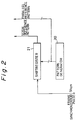
- Fig. 2 shows an example of a construction of the pattern generation circuit 10 in accordance with the embodiment shown in Fig. 1.
- the pattern generation circuit 10 is equipped with a pattern generator 20 and a shift register 21 which is connected thereto.
- the pattern generator 20 generates and outputs in parallel a reference synchronization pattern having the same pattern as a frame synchronization pattern added on the transmission side, for example, the length of the reference synchronization pattern being 16 bits.
- the parallel reference synchronization pattern being outputted is applied to both the shift register 21 and the comparison circuit 11 (Fig. 1).
- the shift register 21 which is a PISO (Parallel-In-Serial-Out) shift register receives the parallel reference synchronization pattern from the pattern generator 20 each time when the frame synchronization pulse Sfsyn is received and then outputs the reference synchronization pattern in series in accordance with a clock pulse of the reception system.
- the serial reference synchronization pattern being outputted is applied to the comparison circuit 11 (Fig. 1).
- the shift register is used as shown in Fig. 2.
- a ROM or synchronization frame demultiplexing circuit may be used instead of the shift register.
- Fig. 3 shows an example of a construction of the comparison circuit 11 in accordance with the embodiment shown in Fig. 1.
- the comparison circuit 11 is equipped with a frame pattern detection circuit 30 connected to the input terminal 14, a synchronization frame demultiplexing circuit 31 connected to the frame pattern detection circuit 30, an AND gate 32 whose one input terminal is connected to an output terminal of the demultiplexing circuit 31, other terminal being connected to the input terminal 14, and an EXOR (Exclusive OR) gate 33 whose one input terminal is connected to an output terminal of the AND gate 32.
- the other input terminal of the EXOR gate 33 receives the serial reference synchronization pattern sent from the pattern generation circuit 10.
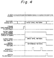
- Fig. 4 is a time chart showing a signal waveform of each portion of the circuits shown in Figs. 1 to 3.
- the frame synchronization pulse Sfsyn when the frame synchronization pulse Sfsyn is applied to the demultiplexing circuit 31, it generates an output Sdem whose signal level is high for the bit length of the frame synchronization pattern added on the transmission side.
- the output Sdem is sent to the frame pattern detection circuit 30 and the AND gate 32.
- the received signal Sin is applied to the EXOR gate 33 in series through the AND gate 32.
- the received signal Sin is compared, bit by bit, with the serial reference synchronization pattern from the pattern generator 20.
- the mismatch pulse Smis is outputted from the EXOR gate 33.
- the frame pattern detection circuit 30 has the same construction as a known and conventional pattern detection circuit. While the signal level of the output Sdem sent from the demultiplexing circuit 31 is high, the received signal Sin, which is the 16-bit input pattern, is compared with the parallel reference synchronization pattern sent from the pattern generator 20. When all the bits of the 16-bit input pattern are matched with those of the parallel reference synchronization pattern, a match pulse Smath is outputted.
- the frame pattern detection circuit 30 can be constructed with a register and a magnitude comparator, for example.
- the match pulse Smath is outputted whereas the mismatch pulse Smis is not outputted.
- a bit error takes place due to a disturbance over the transmission line, a mismatch bit is detected.
- a mismatch pulse Smis is outputted.
- the mismatch bit counter 12 counts the number of the mismatch pulses Smis.
- the match pulses Smath are frequently outputted.
- the mismatch bit counter 12 is reset with the match pulse Smath.
- the out-of frame pulse Sout is not outputted. Consequently, even if a disturbance over the transmission line takes place, an out-of frame hardly takes place.
- the mismatch bit counter 12 counts N mismatch pulses Smis and outputs the out-of frame pulse Sout.
- the probability Pe1 of detecting one mismatch bit in the state where the frames are synchronized in the correct positions is expressed with the following equation.
- Pe1 k C 1 p (1 - p) k-1 where k is the bit length of the synchronization pattern and p is the bit error rate.
- the probability Pej of detecting j mismatch bits is expressed with the following equation.
- Pej k C j p j (1 - p) k-j
- the average quantity Peave of the mismatch pulses Smis which are outputted per frame is expressed with the following equation.
- the probability Pe0 of occurrence of a mismatch bit per frame is expressed with the following equation.
- Pe0 1 - (1 - p) k
- mismatch bit counter 12 when one mismatch of the synchronization patterns takes place, 1.428 mismatch pulses Smis are counted.
- the required size n of mismatch counter was n > 31.75 ⁇ 32.
- the mismatch bit counter 12 according to the present invention should output one mismatch pulse Smis at each time when 31.75 mismatches of the synchronization patterns successively take place on the average. In other words, since 31.75 x 1.428 ⁇ 45.34, the size N of the mismatch bit counter 12 should be 46.
- the mismatch bit counter 12 counts the number of mismatch bits, the degree of freedom of selecting the threshold value X of synchronization determination is high as well as the conventional front synchronization stabilizer.
- Fig. 5 schematically shows a construction of a racing counter type front synchronization stabilizer of another embodiment of the frame synchronization stabilizer according to the present invention.
- a synchronization pattern generation circuit 50 is connected to a comparison circuit 51 to which a received signal is applied.
- the comparison circuit 51 is connected to both a mismatch bit counter 52 for counting a mismatch pulse Smis and a match counter 55.
- Reset input terminals R of the counters 52 and 55 are connected to an output terminal of an OR gate 53.
- Input terminals of the OR gate 53 are connected to carry output terminals CARY of the counters 52 and 55.
- the pattern generation circuit 50 generates a reference synchronization pattern having the same pattern as a frame synchronization pattern added on a transmission side.
- the reference synchronization pattern from the circuit 50 and a received signal Sin from an input terminal 54 are applied to the comparison circuit 51.
- the circuit 51 compares, bit by bit, a signal pattern in a synchronization pattern area of each received frame with the reference synchronization pattern.
- the circuit 51 outputs a mismatch pulse Smis each time when it detects a mismatch bit, and outputs a match pulse Smath each time when it detects that the input signal pattern is fully matched with the reference synchronization pattern.
- the length of the synchronization pattern is 16 bits, if there are three mismatch bits, the comparison circuit 51 outputs three mismatch pulses Smis.
- the comparison circuit 51 only when all 16 bits of the input signal pattern are matched with those of the reference synchronization pattern, the comparison circuit 51 outputs one match pulse Smath.
- the mismatch pulses Smis outputted in the above mentioned manner are applied to a clock input terminal CK of the mismatch bit counter 52.
- the match pulse Smath is applied to a clock input terminal CK of the match counter 55.
- the counter 52 counts the number of received mismatch pulses Smis and outputs a carry pulse from the carry output terminal CARY when the count value becomes a particular value N.
- the carry pulse is outputted as a pulse Sout which denotes that an out-of frame is detected.
- the counter 55 counts the number of received match pulses Smath and outputs a carry pulse from the carry output terminal CARY when the count value becomes a particular value M.
- the out-of frame pulse Sout from the mismatch bit counter 52 and the carry pulse from the match counter 55 are applied to the reset input terminals R of the counters 52 and 55.
- the counters 52 and 55 are reset with the out-of frame pulse Sout from the counter 55 and the carry pulse from the counter 55, respectively.
- the counters 52 and 55 start counting the number of the mismatch pulses Smis and that of the match pulses Smath from "0", respectively.
- the out-of frame pulse Sout is outputted only when N mismatch pulses Smis are successively generated without generation of the carry pulse from the match counter 55.
- a reframing is executed in a known method.
- the mismatch counter is reset. Therefore, in the front synchronization stabilizer according to the embodiment, the out-of frame pulse Sout is outputted when the density of the mismatch pulses Smis in successive frames including N mismatch pulses Smis exceeds N / (N + M - 1).
- the threshold value of out-of frame determination just depends on the mismatch bit counter 12.
- the racing counter type front synchronization stabilizer since the two counters 52 and 55 are provided, it is possible to variably set the threshold value X of out-of frame determination. Thus, the degree of freedom of this stabilizer is higher than that of the related art.
- Fig. 6 shows a transmission data format of another embodiment of the frame synchronization stabilizer according to the present invention.
- data in each frame having the same pattern as a synchronization pattern is transmitted after inverting the synchronization pattern frame by frame so that the synchronization pattern can be identified at the reception side.
- a racing counter type front synchronization stabilizer shown in Fig. 5 is used in this embodiment.
- a data stream with data patterns 61a, 61b, 61c, 61d, ... , etc. which have a pattern NA same as synchronization patterns 60a, 60c, ... , etc. disposed at the beginning of each frame but not the synchronization pattern is transmitted.
- the synchronization patterns 60a, 62b, 60c, 62d, ... , etc. are alternately inverted as shown by NA (normal pattern) and IA (inverted pattern) in Fig. 6 at the transmission side and then transmitted. In such the system, only the synchronization pattern portion should be inverted again at the reception side so as to form a non-inverted synchronization pattern stream.
- Fig. 7 shows an example of a re-inversion circuit disposed upstream of the racing counter type front synchronization stabilizer shown in Fig. 5.
- a received signal inputted through an input terminal 70 is applied to one input terminal of an EXOR gate 71, and a signal from a frame counter 73 through a switch 72 is applied to the other input terminal of the EXOR gate 71.
- the frame counter 73 outputs a high level signal and a low level signal on alternate frames to the switch 72 through a line 72.
- the control signal of the switch 72 places the switch 72 in the position connected to the frame counter 73.
- the control signal places the switch 72 in the position connected to the ground side.
- the portion of the inverted pattern IA of the synchronization pattern is inverted again and thereby the normal pattern NA is outputted.
- the portion of the normal pattern NA which has not been inverted, is outputted as it is. Consequently, the synchronization pattern portion is formed as non-inverted synchronization pattern stream. This pattern stream is sent to the racing counter type front synchronization stabilizer and then the synchronization is stabilized.
- the probability of occurrence of an out-of frame becomes as follows.
- the size n of match counter should be 63.
- mismatch bit counter 52 counts the pulses at a speed approximately 16 times faster than that of the related art.
- the size m of match counter is larger than the size n of mismatch counter (namely, m > n)
- an out-of frame does not take place and thereby the front stabilizing function does not work.
- such a condition is represented by the following relationship between the size M (number of count frames) of match counter 55 and the division N/k of the size N of mismatch bit counter 52 by the bit length k of synchronization pattern.
- M N / k
- the following value is obtained.
- M 10 > N / k ⁇ 5.6
Landscapes
- Engineering & Computer Science (AREA)
- Computer Networks & Wireless Communication (AREA)
- Signal Processing (AREA)
- Synchronisation In Digital Transmission Systems (AREA)
- Time-Division Multiplex Systems (AREA)
Claims (9)
- Stabilisateur de synchronisation de trame pour stabiliser la synchronisation de trame de données reçues, comprenant:des moyens (10) pour générer un motif de référence qui est identique à une synchronisation de trame prédéterminée contenue dans des données transmises;des moyens de comparaison (11, 51) pour comparer un motif de données dans une zone de motif de synchronisation de chaque trame des données reçues à des bits correspondants du motif de référence provenant desdits moyens de génération (10);caractérisé en ce que lesdits moyens de comparaison (11, 51) délivrent une impulsion de non coïncidence (Smis) à chaque fois qu'un bit non coïncident est détecté pendant la comparaison série, bit par bit, et délivrent une impulsion de coïncidence (Smath) à chaque fois qu'il est détecté que le motif de données coïncide totalement avec le motif de référence; et
un premier compteur (12, 53) est prévu pour compter le nombre des impulsions de non coïncidence (Smis) provenant desdits moyens de comparaison (11, 51) et pour délivrer un signal de détection de perte ou sortie de trame (Sout) lorsque le nombre compté dépasse une valeur particulière, et ledit premier compteur est adapté pour être remis à zéro lorsque lesdits moyens de comparaison (11, 51) ont délivré un nombre prédéterminé d'impulsions de coïncidence (Smath). - Stabilisateur de synchronisation de trame selon la revendication 1, dans lequel ledit premier compteur (11) est remis à zéro par l'impulsion de coïncidence délivrée par lesdits moyens de comparaison.
- Stabilisateur de synchronisation de trame selon la revendication 2, dans lequel ledit premier compteur est aussi remis à zéro par le signal de détection de sortie de trame qu'il délivre.
- Stabilisateur de synchronisation de trame selon la revendication 1, comprenant également un second compteur (55) pour compter le nombre des impulsions de coïncidence (Smath) provenant desdits moyens de comparaison (51), ledit second compteur (55) délivrant un signal lorsqu'une valeur comptée dépasse une valeur particulière, lesdits premier et second compteurs (52 et 55) étant remis à zéro par le signal délivré par ledit second compteur (55).
- Stabilisateur de synchronisation de trame selon la revendication 4, dans lequel lesdits premier et second compteurs sont aussi remis à zéro tous les deux par le signal de détection de sortie de trame (Sout) délivré par ledit premier compteur (52).
- Stabilisateur de synchronisation de trame selon la revendication 1, dans lequel lesdits moyens de génération (10) incluent un générateur de motif de synchronisation (20) pour générer un motif de référence parallèle, et des moyens (21) pour convertir le motif de référence parallèle en un motif de référence série.
- Stabilisateur de synchronisation de trame selon la revendication 6, dans lequel lesdits moyens de conversion (21) incluent un registre à décalage de type PISO (registre à décalage à entrée parallèle et sortie série).
- Stabilisateur de synchronisation de trame selon la revendication 1 ou 6, dans lequel lesdits moyens de comparaison (11, 51) incluent un circuit de comparaison de motifs (30) pour délivrer une impulsion de coïncidence (Smath) à chaque fois qu'il est détecté que le motif de données coïncide totalement avec le motif de référence, et un circuit série de comparaison de bits (33) pour délivrer une impulsion de non coïncidence (Smis) à chaque fois qu'un bit non coïncident est détecté par une comparaison série, bit par bit, d'un motif de données dans une zone de motif de synchronisation de chaque trame des données reçues au motif de référence série provenant desdits moyens de génération.
- Stabilisateur de synchronisation de trame selon la revendication 8, dans lequel ledit circuit série de comparaison de bits (33) inclut une porte OU exclusif recevant le motif de données en série et le motif de référence série, ladite porte OU exclusif délivrant l'impulsion de non coïncidence à chaque fois qu'un bit du motif de données et un bit du motif de référence série ne coïncident pas.
Applications Claiming Priority (2)
| Application Number | Priority Date | Filing Date | Title |
|---|---|---|---|
| JP95852/90 | 1990-04-10 | ||
| JP2095852A JPH0771060B2 (ja) | 1990-04-10 | 1990-04-10 | フレーム同期保護回路 |
Publications (3)
| Publication Number | Publication Date |
|---|---|
| EP0451767A2 EP0451767A2 (fr) | 1991-10-16 |
| EP0451767A3 EP0451767A3 (en) | 1992-07-08 |
| EP0451767B1 true EP0451767B1 (fr) | 1996-09-11 |
Family
ID=14148903
Family Applications (1)
| Application Number | Title | Priority Date | Filing Date |
|---|---|---|---|
| EP91105555A Expired - Lifetime EP0451767B1 (fr) | 1990-04-10 | 1991-04-08 | Stabilisateur de synchronisation de trâme |
Country Status (4)
| Country | Link |
|---|---|
| US (1) | US5228036A (fr) |
| EP (1) | EP0451767B1 (fr) |
| JP (1) | JPH0771060B2 (fr) |
| DE (1) | DE69121952T2 (fr) |
Families Citing this family (14)
| Publication number | Priority date | Publication date | Assignee | Title |
|---|---|---|---|---|
| KR0136568B1 (ko) * | 1992-07-23 | 1998-11-16 | 강진구 | D2 mac신호의 프레임동기검출방법 및 장치 |
| US5463627A (en) * | 1993-02-23 | 1995-10-31 | Matsushita Electric Industrial Co., Ltd. | Frame synchronizing apparatus for quadrature modulation data communication radio receiver |
| JP2626551B2 (ja) * | 1994-05-18 | 1997-07-02 | 日本電気株式会社 | 誤り許容パターンマッチング回路 |
| DE4429595C1 (de) * | 1994-08-20 | 1995-06-29 | Philips Patentverwaltung | Übertragungssystem zur Übertragung und zur Erkennung des Rahmenanfangs eines rahmensynchronisierten Signals |
| US5661763A (en) * | 1995-07-28 | 1997-08-26 | Adtran, Inc. | Apparatus and method for detecting programmable length bit pattern in serial digital data stream |
| US6567424B1 (en) * | 1995-08-07 | 2003-05-20 | Motorola, Inc. | Apparatus and method for determining a synchronization signal |
| US5748686A (en) * | 1996-04-04 | 1998-05-05 | Globespan Technologies, Inc. | System and method producing improved frame synchronization in a digital communication system |
| JP3322561B2 (ja) * | 1996-04-12 | 2002-09-09 | シャープ株式会社 | Fm文字多重放送用受信機 |
| US5870444A (en) * | 1996-04-23 | 1999-02-09 | Scientific-Atlanta, Inc. | Method and apparatus for performing very fast message synchronization |
| US6980617B1 (en) * | 2000-11-15 | 2005-12-27 | Advantest Corporation | Reception data synchronizing apparatus and method, and recording medium with recorded reception data synchronizing program |
| JP3875478B2 (ja) * | 2000-10-13 | 2007-01-31 | 富士通株式会社 | 同期判別装置および通信システム |
| US6907045B1 (en) * | 2000-11-17 | 2005-06-14 | Nortel Networks Limited | Method and apparatus for data-path conversion comprising PCM bit robbing signalling |
| KR100575710B1 (ko) * | 2002-07-20 | 2006-05-03 | 엘지전자 주식회사 | 업링크 동기 검출방법 |
| JP4984054B2 (ja) * | 2007-03-19 | 2012-07-25 | 日本電気株式会社 | フレーム同期装置およびフレーム同期方法 |
Family Cites Families (9)
| Publication number | Priority date | Publication date | Assignee | Title |
|---|---|---|---|---|
| US3537069A (en) * | 1967-10-02 | 1970-10-27 | Gen Dynamics Corp | Sychronizers employing sequential probability ratio tests |
| US4002845A (en) * | 1975-03-26 | 1977-01-11 | Digital Communications Corporation | Frame synchronizer |
| US4404675A (en) * | 1981-04-27 | 1983-09-13 | Gte Automatic Electric Incorporated | Frame detection and synchronization system for high speed digital transmission systems |
| JPS61158780U (fr) * | 1985-03-22 | 1986-10-01 | ||
| NZ220548A (en) * | 1986-06-18 | 1990-05-28 | Fujitsu Ltd | Tdm frame synchronising circuit |
| US4768192A (en) * | 1987-04-01 | 1988-08-30 | General Signal Corp. | Frame synchronization detection system for time division multiplexed (TDM) digital signals |
| JPH0828691B2 (ja) * | 1988-03-14 | 1996-03-21 | 富士通株式会社 | フレーム同期方式 |
| KR910005493B1 (ko) * | 1988-12-14 | 1991-07-31 | 한국전기통신공사 | 동기식 다중화 장치의 리프레임 회로 |
| DE3842694A1 (de) * | 1988-12-19 | 1990-06-21 | Standard Elektrik Lorenz Ag | Demultiplexer mit schaltung zur verringerung des wartezeitjitters |
-
1990
- 1990-04-10 JP JP2095852A patent/JPH0771060B2/ja not_active Expired - Lifetime
-
1991
- 1991-04-08 DE DE69121952T patent/DE69121952T2/de not_active Expired - Fee Related
- 1991-04-08 EP EP91105555A patent/EP0451767B1/fr not_active Expired - Lifetime
- 1991-04-10 US US07/683,454 patent/US5228036A/en not_active Expired - Fee Related
Also Published As
| Publication number | Publication date |
|---|---|
| EP0451767A3 (en) | 1992-07-08 |
| EP0451767A2 (fr) | 1991-10-16 |
| DE69121952T2 (de) | 1997-03-13 |
| US5228036A (en) | 1993-07-13 |
| JPH03293829A (ja) | 1991-12-25 |
| JPH0771060B2 (ja) | 1995-07-31 |
| DE69121952D1 (de) | 1996-10-17 |
Similar Documents
| Publication | Publication Date | Title |
|---|---|---|
| JP4207329B2 (ja) | フレーム同期回路 | |
| CA1167185A (fr) | Circuit de resynchronisation de cadres pour recepteur numerique | |
| EP0096854B1 (fr) | Système de synchronisation de trâme | |
| US4225960A (en) | Automatic synchronizing system for digital asynchronous communications | |
| US4920535A (en) | Demultiplexer system | |
| US4214124A (en) | Method and device for extracting a synchronizing signal from an incoming PCM signal | |
| US5228036A (en) | Frame synchronization stabilizer | |
| US4404675A (en) | Frame detection and synchronization system for high speed digital transmission systems | |
| US4158193A (en) | Data transmission test set with synchronization detector | |
| US3978285A (en) | Frame synchronizing device | |
| US6693919B1 (en) | Frame synchronization method and frame synchronization circuit | |
| US4646328A (en) | Frame alignment loss and recovery device for a digital signal | |
| US4203003A (en) | Frame search control for digital transmission system | |
| US5113417A (en) | Frame detection system | |
| US5208840A (en) | Method and arrangement for detecting framing bit sequence in digital data communications system | |
| US4394758A (en) | Synchronizing unit for receiving section of PCM station | |
| US5062107A (en) | Synchronizing circuit for reducing waiting-time jitter in a demultiplexer | |
| AU639731B2 (en) | A flywheel circuit | |
| JP2716392B2 (ja) | フレーム同期回路 | |
| JPS585543B2 (ja) | フレ−ム同期装置 | |
| JPH0630479B2 (ja) | フレ−ム同期方式 | |
| JP3290331B2 (ja) | ブロック同期処理回路 | |
| US6307904B1 (en) | Clock recovery circuit | |
| JP2870314B2 (ja) | 伝送路誤り率劣化警報検出回路 | |
| JPH0614640B2 (ja) | フレ−ム同期回路 |
Legal Events
| Date | Code | Title | Description |
|---|---|---|---|
| PUAI | Public reference made under article 153(3) epc to a published international application that has entered the european phase |
Free format text: ORIGINAL CODE: 0009012 |
|
| AK | Designated contracting states |
Kind code of ref document: A2 Designated state(s): DE FR GB |
|
| PUAL | Search report despatched |
Free format text: ORIGINAL CODE: 0009013 |
|
| AK | Designated contracting states |
Kind code of ref document: A3 Designated state(s): DE FR GB |
|
| 17P | Request for examination filed |
Effective date: 19920929 |
|
| 17Q | First examination report despatched |
Effective date: 19940914 |
|
| GRAH | Despatch of communication of intention to grant a patent |
Free format text: ORIGINAL CODE: EPIDOS IGRA |
|
| GRAA | (expected) grant |
Free format text: ORIGINAL CODE: 0009210 |
|
| GRAH | Despatch of communication of intention to grant a patent |
Free format text: ORIGINAL CODE: EPIDOS IGRA |
|
| AK | Designated contracting states |
Kind code of ref document: B1 Designated state(s): DE FR GB |
|
| REF | Corresponds to: |
Ref document number: 69121952 Country of ref document: DE Date of ref document: 19961017 |
|
| ET | Fr: translation filed | ||
| PLBE | No opposition filed within time limit |
Free format text: ORIGINAL CODE: 0009261 |
|
| STAA | Information on the status of an ep patent application or granted ep patent |
Free format text: STATUS: NO OPPOSITION FILED WITHIN TIME LIMIT |
|
| 26N | No opposition filed | ||
| PGFP | Annual fee paid to national office [announced via postgrant information from national office to epo] |
Ref country code: DE Payment date: 20010402 Year of fee payment: 11 |
|
| PGFP | Annual fee paid to national office [announced via postgrant information from national office to epo] |
Ref country code: GB Payment date: 20010404 Year of fee payment: 11 |
|
| PGFP | Annual fee paid to national office [announced via postgrant information from national office to epo] |
Ref country code: FR Payment date: 20010409 Year of fee payment: 11 |
|
| REG | Reference to a national code |
Ref country code: GB Ref legal event code: IF02 |
|
| PG25 | Lapsed in a contracting state [announced via postgrant information from national office to epo] |
Ref country code: GB Free format text: LAPSE BECAUSE OF NON-PAYMENT OF DUE FEES Effective date: 20020408 |
|
| PG25 | Lapsed in a contracting state [announced via postgrant information from national office to epo] |
Ref country code: DE Free format text: LAPSE BECAUSE OF NON-PAYMENT OF DUE FEES Effective date: 20021101 |
|
| GBPC | Gb: european patent ceased through non-payment of renewal fee |
Effective date: 20020408 |
|
| PG25 | Lapsed in a contracting state [announced via postgrant information from national office to epo] |
Ref country code: FR Free format text: LAPSE BECAUSE OF NON-PAYMENT OF DUE FEES Effective date: 20021231 |
|
| REG | Reference to a national code |
Ref country code: FR Ref legal event code: ST |