EP0451856A1 - Détecteur d'images à l'état solide - Google Patents
Détecteur d'images à l'état solide Download PDFInfo
- Publication number
- EP0451856A1 EP0451856A1 EP91105833A EP91105833A EP0451856A1 EP 0451856 A1 EP0451856 A1 EP 0451856A1 EP 91105833 A EP91105833 A EP 91105833A EP 91105833 A EP91105833 A EP 91105833A EP 0451856 A1 EP0451856 A1 EP 0451856A1
- Authority
- EP
- European Patent Office
- Prior art keywords
- voltage
- image sensing
- solid
- sensing device
- state image
- Prior art date
- Legal status (The legal status is an assumption and is not a legal conclusion. Google has not performed a legal analysis and makes no representation as to the accuracy of the status listed.)
- Granted
Links
Images


Classifications
-
- H—ELECTRICITY
- H10—SEMICONDUCTOR DEVICES; ELECTRIC SOLID-STATE DEVICES NOT OTHERWISE PROVIDED FOR
- H10F—INORGANIC SEMICONDUCTOR DEVICES SENSITIVE TO INFRARED RADIATION, LIGHT, ELECTROMAGNETIC RADIATION OF SHORTER WAVELENGTH OR CORPUSCULAR RADIATION
- H10F39/00—Integrated devices, or assemblies of multiple devices, comprising at least one element covered by group H10F30/00, e.g. radiation detectors comprising photodiode arrays
- H10F39/10—Integrated devices
- H10F39/12—Image sensors
- H10F39/15—Charge-coupled device [CCD] image sensors
- H10F39/158—Charge-coupled device [CCD] image sensors having arrangements for blooming suppression
-
- H—ELECTRICITY
- H10—SEMICONDUCTOR DEVICES; ELECTRIC SOLID-STATE DEVICES NOT OTHERWISE PROVIDED FOR
- H10F—INORGANIC SEMICONDUCTOR DEVICES SENSITIVE TO INFRARED RADIATION, LIGHT, ELECTROMAGNETIC RADIATION OF SHORTER WAVELENGTH OR CORPUSCULAR RADIATION
- H10F39/00—Integrated devices, or assemblies of multiple devices, comprising at least one element covered by group H10F30/00, e.g. radiation detectors comprising photodiode arrays
- H10F39/80—Constructional details of image sensors
-
- H—ELECTRICITY
- H04—ELECTRIC COMMUNICATION TECHNIQUE
- H04N—PICTORIAL COMMUNICATION, e.g. TELEVISION
- H04N25/00—Circuitry of solid-state image sensors [SSIS]; Control thereof
- H04N25/60—Noise processing, e.g. detecting, correcting, reducing or removing noise
- H04N25/62—Detection or reduction of noise due to excess charges produced by the exposure, e.g. smear, blooming, ghost image, crosstalk or leakage between pixels
- H04N25/621—Detection or reduction of noise due to excess charges produced by the exposure, e.g. smear, blooming, ghost image, crosstalk or leakage between pixels for the control of blooming
- H04N25/622—Detection or reduction of noise due to excess charges produced by the exposure, e.g. smear, blooming, ghost image, crosstalk or leakage between pixels for the control of blooming by controlling anti-blooming drains
-
- H—ELECTRICITY
- H10—SEMICONDUCTOR DEVICES; ELECTRIC SOLID-STATE DEVICES NOT OTHERWISE PROVIDED FOR
- H10W—GENERIC PACKAGES, INTERCONNECTIONS, CONNECTORS OR OTHER CONSTRUCTIONAL DETAILS OF DEVICES COVERED BY CLASS H10
- H10W20/00—Interconnections in chips, wafers or substrates
- H10W20/40—Interconnections external to wafers or substrates, e.g. back-end-of-line [BEOL] metallisations or vias connecting to gate electrodes
- H10W20/49—Adaptable interconnections, e.g. fuses or antifuses
- H10W20/493—Fuses, i.e. interconnections changeable from conductive to non-conductive
Definitions
- the present invention relates to a solid-state image sensing device.
- the input condition thereto changes according to the luminance of a subject to be sensed. Therefore, when a subject of a high luminance is image-sensed, since an excessive. electric charge transduced from light energy by the photodiode section of the device leaks to the vertical register, so that a phenomenon can be observed such that light spreads on a monitor picture from a high luminance position to a low luminance position. This phenomenon is referred to as blooming phenomenon. To prevent this phenomenon, an overflow drain is conventionally provided for the image sensing device.
- Fig. 5 is a sectional diagram of a solid-state image sensing device having an overflow drain, which is conventionally used.
- An n region 20 is formed in the surface of a p-type silicon substrate 10.
- a p-n junction formed by the n region and the substarate forms a photo diode. If light 30 is irradiated at this photo diode, electric charges are generated at the photo diode and in response to open/close state of a transfer gate 50, these electric charges are moved to a CCD section 40 which stores and transferrs the charges.
- an overflow drain 60 is provided at the other side of the photo diode. Amount of excessive electric charges is controlled by a voltage applied to a gate 70.
- Fig. 6 shows the relationship between the blooming rate and the voltage V OFD applied to the gate provided for the overflow drain.
- the overflow drain voltage V OFD is sufficiently high as within a range A, since the blooming phenomenon can be sufficiently suppressed, it is possible to extremely reduce the blooming rate in the case where high luminance subject is image-sensed.
- the overflow drain voltage V OFD is low as within a range B, since the blooming phenomenon cannot be sufficiently suppressed, the blooming phenomenon is observed.
- the lower limit of the overflow drain voltage V OFD at which the blooming phenomenon can be suppressed is a point C corresponding to a boundary between the two ranges A and B. Therefore, the range A of the overflow drain voltage V OFD is a practical voltage range.
- the overflow drain voltage V OFD exerts an influence upon the saturation characteristics in relation to the quantity of electric charge to be accumulated.
- Fig. 7 shows the relationship between the overflow drain voltage V OFD and the saturation voltage obtained by converting the quantity of accumulated electric charge.
- To increase the saturation voltage it is desirable to reduce the overflow drain voltage V OFD .
- since there exists a limit of the quantity of accumulated electric charge it is impossible to increase the electric charge quantity beyond the limit, even if the voltage V OFD is reduced unnecessarily.
- the saturation voltage V OFD is required to be higher than a white-clip level when the image signals are processed. Therefore, although it is effective to determine a higher overflow drain voltage V OFD in order to sufficiently suppress the blooming phenomenon, since the lower overflow drain voltage or the higher saturation voltage is required for signal processing, the overflow drain voltage V OFD is usually set to a point E higher than the lower limit point C. Accordingly, the saturation voltage D at a point E of the overflow drain voltage V OFD is lower than the voltage F at the point C of V OFD .
- the overflow drain voltage V OFD is adjusted according to the usage. Further, since this voltage V OFD differs according to the manufacturing process, the voltage V OFD ranges between several volts and tens and several volts.
- each solid-state image sensing device is inspected at the wafer stage in order to detect an optimum overflow drain voltage V OFD .
- V OFD overflow drain voltage
- an optimum overflow drain voltage V OFD is indicated on a predetermined position 702 of a casing 701 of a solid-state image sensing device, as shown in Fig. 8, in order to eliminate the waste inspection work. That is, when the solid-state image sensing device is assembled in an apparatus (e.g. camera), an optimum overflow drain voltage is applied to the image sensing device by reading the previously indicated V OFD .
- an apparatus e.g. camera
- the prior-art method of indicating various optimum voltages by stamping work for instance is very troublesome in mass-production process, in particular. This is because since the optimum overflow drain voltage V OFD of the devices differ from each other as already explained, the optimum voltages must be classified into about several tens of ranges at 0.5V intervals in general before stamping the indication values. Where the abovementioned troublesome work is performed by workers, the efficiency is extremely low and further there exists a problem in that error is inevitably produced during the classification and stamping work.
- the automation system may be extremely high in both development and manufacturing cost, because the optimum values inspected in the inspection process must be stored in relation to the corresponding devices and further stamped on the corresponding devices.
- the object of the present invention provides a solid-state image sensing device which can reduce the optimum operating voltage indicating work, without use of any automatic voltage indicating system.
- the present invention provides a solid-state image sensing device, comprising: photoelectric transducing means for generating electric charges corresponding to incident light intensity; charge transferring means for accumulating and transferring electric charge generated by said photoelectric transducing means; and voltage generating means responsive to an external voltage selecting signal, for generating a voltage corresponding to the voltage selecting signal and lying within a predetermined range.
- the voltage generating means whenever an external voltage selecting signal is inputted to the device, the voltage generating means generates a voltage corresponding to the inputted voltage selecting signal and lying within a predetermined range. Since the above-mentioned voltage generating means is formed in the solid-state image sensing device, a required operating voltage can be generated by the device itself. Therefore, it is unnecessary to indicate the voltage on the device casing, and further it is possible to directly use the generated voltage for device activation.
- the voltage generated by the voltage generating means is preferably the voltage applied to the overflow drain of the device.
- the voltage generating means is a resistance divider circuit
- the resistance between a voltage supply terminal and a ground terminal changes, so that a voltage corresponding to the inputted voltage selecting signal is generated at the connection end of the series-connected resistors.
- the solid-state image sensing device is provided with means for generating a voltage determined in response to a voltage selecting signal inputted to the device from outside, it is possible to generate a necessary voltage from the device itself, thus eliminating the indication of device voltage on the device surface. Therefore, it is unnecessary to develop a new automatic voltage indicating system for automatically stamping operating voltages on the device casings, by spending much development cost therefor.
- the solid-state image sensing device is provided with means for generating a voltage lying within a predetermined range.
- This voltage generating means is so controlled as to generate an optimum overflow drain voltage V OFD in response to an external signal.
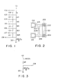
- Fig. 1 shows the voltage generating means provided for the solid-state image sensing device according to the present invention.
- the voltage generating means is a resistance divider circuit for generating any required voltage.
- a plurality of resistors R, 2R, 4R, 8R, 16R, 32R and (63 x 7/8)R are connected in series between a voltage supply terminal 101 and a ground 120.
- the resistance values of these resistors 2R to 32R are determined into two's multiple arrangement.
- each of a plurality of fuses 109 to 114 are connected in parallel to each of the resistors R to 32R.
- the resistor R and the fuse 109 are both connected between two fusing terminals 102 and 103; the resistor 2R and the fuse 110 are connected between two fusing terminals 103 and 104; the resistor 4R and the fuse 111 are both connected between two fusing terminals 104 and 105; the resistor 8R and the fuse 112 are both connected between two fusing terminals 105 and 106; the resistor 16R and the fuse 113 are both connected between two fusing terminals 106 and 107; and the resistor 32R and the fuse 114 are both connected between two fusing terminals 107 and 108, respectively.
- an overflow drain voltage V OFD required to be generated can be outputted through an output terminal 108.
- Fig. 2 is an enlarged view showing the resistor R and the fuse 109 both formed on a semiconductor substrate, by way of example.
- n+ diffusion layers 203 and 204 are formed on both ends of a gate region 202, and an n diffusion layer 201 constituting the resistor R is formed between the two n+ diffusion layers 203 and 204.
- These two n+ diffusion layers 203 and 204 are connected to two aluminium wires 205 and 206 via two contacts 203 and 204, respectively at each one end thereof, and the two fusing terminals 102 and 103 are formed on the wires 205 and 206, respectively at each other end thereof.
- the two aluminium wires 205 and 206 are connected to each other via a bridge wire 203 formed with a narrower portion 209. Since being high in resistance, this narrower portion 209 corresponds to a fuse 109 melted away when a predetermined high voltage is applied between the two fusing terminals 102 and 103.
- any desired voltages can be outputted through the output terminal 108 by selecting the resistance of the series-connected resistors R to 32R as follows: For instance, the assumption is made that a voltage of 10.00V is required to be outputted through the output terminal 108 when a supply voltage of 15.00V is applied to the voltage supply terminal 101, as shown by an equivalent circuit in Fig. 3.
- the third, fourth and fifth resistors 4R, 8R and 16R are to be selected in order to obtain a resistance 28R between the voltage supply terminal 101 and the output terminal 108. That is, the fuses 111, 112 and 113 must be melted away to allow current to flow through the three resistors 4R, 8R and 16R. Therefore, these three fuses 111, 112 and 113 are melted by passing fusing current between the two fusing terminals of 104 and 105, 105 and 106, and 106 and 107, respectively.
- fusing code C a sum total resistance to be selected.
- Fig. 4 shows the relationship between the fusing code C as expressed by the formula (2) and the overflow drain voltage V OFD . Therefore, it is possible to easily obtain any required fusing code C by use of the graph as shown in Fig. 4.
- Fig. 4 indicates that the voltage range obtainable through the output terminal 108 is from 7 to 15 volts. However, this voltage range can be changed easily by adjusting the supply voltage applied to the voltage supply terminal 101 and the resistances of the respective resistors.
- the voltage generating means is not limited to only the resistance divider circuit as shown in Fig. 1, but any voltage generating means for generating any required operating voltages in response to external signals can be adopted.
- the generated voltage is not limited to only the overflow drain voltage, but the reset voltage can be generated.
- the device is provided with means for outputting the generated voltage externally. That is, it is possible to directly apply the generated voltage to the overflow drain within the device itself. In this case, it is also possible to reduce the device cost, without need of any automatic voltage indicating system.
Landscapes
- Engineering & Computer Science (AREA)
- Multimedia (AREA)
- Signal Processing (AREA)
- Transforming Light Signals Into Electric Signals (AREA)
- Solid State Image Pick-Up Elements (AREA)
- Semiconductor Integrated Circuits (AREA)
Applications Claiming Priority (2)
| Application Number | Priority Date | Filing Date | Title |
|---|---|---|---|
| JP97887/90 | 1990-04-13 | ||
| JP2097887A JP2601933B2 (ja) | 1990-04-13 | 1990-04-13 | 固体撮像装置 |
Publications (2)
| Publication Number | Publication Date |
|---|---|
| EP0451856A1 true EP0451856A1 (fr) | 1991-10-16 |
| EP0451856B1 EP0451856B1 (fr) | 1997-08-06 |
Family
ID=14204263
Family Applications (1)
| Application Number | Title | Priority Date | Filing Date |
|---|---|---|---|
| EP91105833A Expired - Lifetime EP0451856B1 (fr) | 1990-04-13 | 1991-04-12 | Méthode de fabrication d'un détecteur d'images à l'état solide |
Country Status (5)
| Country | Link |
|---|---|
| US (1) | US5150216A (fr) |
| EP (1) | EP0451856B1 (fr) |
| JP (1) | JP2601933B2 (fr) |
| KR (1) | KR950006048B1 (fr) |
| DE (1) | DE69127120T2 (fr) |
Cited By (5)
| Publication number | Priority date | Publication date | Assignee | Title |
|---|---|---|---|---|
| EP0494104A3 (fr) * | 1991-01-04 | 1992-12-30 | Sharp Kabushiki Kaisha | Capteur d'images CCD |
| EP0747956A3 (fr) * | 1995-06-08 | 1999-03-24 | Matsushita Electronics Corporation | Dispositif semi-conducteur comportant un générateur de tension réglable |
| SG81896A1 (en) * | 1995-06-08 | 2001-07-24 | Matsushita Electronics Corp | Semiconductor device containing an adjustable voltage generator |
| WO2008011064A3 (fr) * | 2006-07-19 | 2008-05-08 | Eastman Kodak Co | Ccd avec circuit de réglage de tension de substrat perfectionné |
| EP1566831A3 (fr) * | 2004-02-18 | 2009-02-25 | Ricoh Company, Ltd. | Dispositif a semi-conducteurs et procédé de fabrication dudit dispositif |
Families Citing this family (12)
| Publication number | Priority date | Publication date | Assignee | Title |
|---|---|---|---|---|
| JP2659456B2 (ja) * | 1990-10-03 | 1997-09-30 | シャープ株式会社 | 固体撮像素子 |
| JP2001077310A (ja) * | 1999-09-01 | 2001-03-23 | Mitsubishi Electric Corp | 電圧設定回路 |
| JP2005277398A (ja) * | 2004-02-25 | 2005-10-06 | Sony Corp | Ccdリニアセンサ |
| JP4740771B2 (ja) * | 2006-03-03 | 2011-08-03 | 株式会社リコー | 分圧回路、その分圧回路を使用した定電圧回路及び電圧検出回路、分圧回路のトリミング方法 |
| TWI328150B (en) * | 2007-03-06 | 2010-08-01 | Neotec Semiconductor Ltd | Binary bidirectional trimming circuit |
| JP2008263088A (ja) * | 2007-04-12 | 2008-10-30 | Rohm Co Ltd | 半導体装置 |
| JP5266800B2 (ja) * | 2008-03-06 | 2013-08-21 | 株式会社リコー | トリミング回路 |
| CN101644937B (zh) * | 2008-08-04 | 2011-11-16 | 新德科技股份有限公司 | 一种利用可调式熔丝调整参考电压的电路 |
| ITMI20110844A1 (it) * | 2011-05-13 | 2012-11-14 | St Microelectronics Srl | Circuito elettronico di trimming |
| TWI484313B (zh) * | 2013-08-05 | 2015-05-11 | Nuvoton Technology Corp | 參考電壓產生電路及其具負電荷保護機制之電壓調整裝置 |
| CN103531576B (zh) * | 2013-10-25 | 2016-05-04 | 无锡中感微电子股份有限公司 | 修调电阻控制装置及使用该装置的晶圆测试系统 |
| US20200373109A1 (en) * | 2019-05-21 | 2020-11-26 | Rosemount Aerospace, Inc. | Fuse assembly and method of making |
Citations (3)
| Publication number | Priority date | Publication date | Assignee | Title |
|---|---|---|---|---|
| US4412241A (en) * | 1980-11-21 | 1983-10-25 | National Semiconductor Corporation | Multiple trim structure |
| GB2177542A (en) * | 1985-07-05 | 1987-01-21 | Gen Electric Plc | Charge coupled device image sensors |
| EP0346905A2 (fr) * | 1988-06-15 | 1989-12-20 | Nec Corporation | Méthode de commande de l'obturateur électronique pour un dispositif de couplage de charge bidimensionnel |
Family Cites Families (12)
| Publication number | Priority date | Publication date | Assignee | Title |
|---|---|---|---|---|
| US4100437A (en) * | 1976-07-29 | 1978-07-11 | Intel Corporation | MOS reference voltage circuit |
| JPS56132815A (en) * | 1980-03-21 | 1981-10-17 | Nec Corp | Reference step voltage generating circuit |
| JPS6020687A (ja) * | 1983-07-15 | 1985-02-01 | Nippon Kogaku Kk <Nikon> | 電子スチルカメラ |
| JPS60128650A (ja) * | 1983-12-15 | 1985-07-09 | Toshiba Corp | 半導体集積回路の基板バイアス発生回路 |
| JPS60236585A (ja) * | 1984-05-10 | 1985-11-25 | Sony Corp | 電子回路の調整方法 |
| JPS6157181A (ja) * | 1984-08-28 | 1986-03-24 | Sharp Corp | 固体撮像装置 |
| EP0186162B1 (fr) * | 1984-12-24 | 1989-05-31 | Kabushiki Kaisha Toshiba | Capteur d'image à l'état solide |
| JPH0714042B2 (ja) * | 1986-02-26 | 1995-02-15 | 三菱電機株式会社 | 固体撮像素子 |
| JP2563370B2 (ja) * | 1986-12-27 | 1996-12-11 | オリンパス光学工業株式会社 | 焦点検出用光電変換装置 |
| JPH0191383U (fr) * | 1987-12-10 | 1989-06-15 | ||
| FR2636800A1 (fr) * | 1988-09-16 | 1990-03-23 | Thomson Csf | Procede de lecture de cellules photosensibles du type comportant deux diodes montees en serie avec des sens de conduction opposes |
| JPH02155378A (ja) * | 1988-12-07 | 1990-06-14 | Nec Corp | 固体撮像素子の駆動方法 |
-
1990
- 1990-04-13 JP JP2097887A patent/JP2601933B2/ja not_active Expired - Fee Related
-
1991
- 1991-04-12 EP EP91105833A patent/EP0451856B1/fr not_active Expired - Lifetime
- 1991-04-12 US US07/684,566 patent/US5150216A/en not_active Expired - Lifetime
- 1991-04-12 KR KR1019910005831A patent/KR950006048B1/ko not_active Expired - Fee Related
- 1991-04-12 DE DE69127120T patent/DE69127120T2/de not_active Expired - Fee Related
Patent Citations (3)
| Publication number | Priority date | Publication date | Assignee | Title |
|---|---|---|---|---|
| US4412241A (en) * | 1980-11-21 | 1983-10-25 | National Semiconductor Corporation | Multiple trim structure |
| GB2177542A (en) * | 1985-07-05 | 1987-01-21 | Gen Electric Plc | Charge coupled device image sensors |
| EP0346905A2 (fr) * | 1988-06-15 | 1989-12-20 | Nec Corporation | Méthode de commande de l'obturateur électronique pour un dispositif de couplage de charge bidimensionnel |
Non-Patent Citations (2)
| Title |
|---|
| ELECTRONICS & WIRELESS WORLD, vol. 95, no. 1641, July 1989, SUTTON, GB; page 661, "Precision analogue signal processing" * |
| IBM TECHNICAL DISCLOSURE BULLETIN, vol. 31, no. 11, April 1989, NEW YORK, US; pages 406 - 410; "High reliability low-cost fuse configuration" * |
Cited By (6)
| Publication number | Priority date | Publication date | Assignee | Title |
|---|---|---|---|---|
| EP0494104A3 (fr) * | 1991-01-04 | 1992-12-30 | Sharp Kabushiki Kaisha | Capteur d'images CCD |
| EP0747956A3 (fr) * | 1995-06-08 | 1999-03-24 | Matsushita Electronics Corporation | Dispositif semi-conducteur comportant un générateur de tension réglable |
| SG81896A1 (en) * | 1995-06-08 | 2001-07-24 | Matsushita Electronics Corp | Semiconductor device containing an adjustable voltage generator |
| EP1566831A3 (fr) * | 2004-02-18 | 2009-02-25 | Ricoh Company, Ltd. | Dispositif a semi-conducteurs et procédé de fabrication dudit dispositif |
| WO2008011064A3 (fr) * | 2006-07-19 | 2008-05-08 | Eastman Kodak Co | Ccd avec circuit de réglage de tension de substrat perfectionné |
| US7508432B2 (en) | 2006-07-19 | 2009-03-24 | Eastman Kodak Company | CCD with improved substrate voltage setting circuit |
Also Published As
| Publication number | Publication date |
|---|---|
| EP0451856B1 (fr) | 1997-08-06 |
| DE69127120D1 (de) | 1997-09-11 |
| JPH03295274A (ja) | 1991-12-26 |
| KR950006048B1 (ko) | 1995-06-07 |
| US5150216A (en) | 1992-09-22 |
| DE69127120T2 (de) | 1998-01-08 |
| JP2601933B2 (ja) | 1997-04-23 |
| KR910019414A (ko) | 1991-11-30 |
Similar Documents
| Publication | Publication Date | Title |
|---|---|---|
| EP0451856B1 (fr) | Méthode de fabrication d'un détecteur d'images à l'état solide | |
| US5619262A (en) | Solid-state image pickup apparatus including a unit cell array | |
| US8218048B2 (en) | Amplifying solid-state imaging device, and method for driving the same | |
| US6797933B1 (en) | On-chip design-for-testing structure for CMOS APS (active pixel sensor) image sensor | |
| US5115124A (en) | Semiconductor photosensor having unitary construction | |
| US20020025164A1 (en) | Solid-state imaging device and electronic camera and shading compensation method | |
| US5010409A (en) | Image sensing system | |
| GB2328338A (en) | Temperature dependent dark current correction in imaging apparatus | |
| JPH05158107A (ja) | 撮像装置用自動測光装置 | |
| US4906855A (en) | Photosensitive matrix with two diodes per dot without specific resetting conductor | |
| US20230358534A1 (en) | Photodetector and distance measuring system | |
| JPH11305112A5 (fr) | ||
| US4039824A (en) | Focus detecting photoelectric device | |
| US20060125945A1 (en) | Solid-state imaging device and electronic camera and shading compensaton method | |
| US4692025A (en) | Semiconductor color sensor detection circuit | |
| CN116998164A (zh) | 电压控制系统 | |
| JP3527911B2 (ja) | 光センサモニタ回路 | |
| US5115321A (en) | Image sensing system | |
| US4633092A (en) | Light sensing device | |
| JPH09138161A (ja) | 光検知素子 | |
| JP4029135B2 (ja) | 光電変換素子及び光電変換装置 | |
| EP1122789A2 (fr) | Capteur d'image utilisant du matériau photosensible pour l'augmentation de la plage dynamique et commande des capteurs d'image | |
| EP1712886A1 (fr) | Dispositif photodetecteur | |
| JPH0528827Y2 (fr) | ||
| CN101295727B (zh) | 图像传感器ic |
Legal Events
| Date | Code | Title | Description |
|---|---|---|---|
| PUAI | Public reference made under article 153(3) epc to a published international application that has entered the european phase |
Free format text: ORIGINAL CODE: 0009012 |
|
| 17P | Request for examination filed |
Effective date: 19910412 |
|
| AK | Designated contracting states |
Kind code of ref document: A1 Designated state(s): DE FR GB |
|
| 17Q | First examination report despatched |
Effective date: 19941026 |
|
| GRAG | Despatch of communication of intention to grant |
Free format text: ORIGINAL CODE: EPIDOS AGRA |
|
| GRAH | Despatch of communication of intention to grant a patent |
Free format text: ORIGINAL CODE: EPIDOS IGRA |
|
| GRAH | Despatch of communication of intention to grant a patent |
Free format text: ORIGINAL CODE: EPIDOS IGRA |
|
| GRAA | (expected) grant |
Free format text: ORIGINAL CODE: 0009210 |
|
| AK | Designated contracting states |
Kind code of ref document: B1 Designated state(s): DE FR GB |
|
| REF | Corresponds to: |
Ref document number: 69127120 Country of ref document: DE Date of ref document: 19970911 |
|
| ET | Fr: translation filed | ||
| PG25 | Lapsed in a contracting state [announced via postgrant information from national office to epo] |
Ref country code: GB Free format text: LAPSE BECAUSE OF NON-PAYMENT OF DUE FEES Effective date: 19980412 |
|
| PLBE | No opposition filed within time limit |
Free format text: ORIGINAL CODE: 0009261 |
|
| STAA | Information on the status of an ep patent application or granted ep patent |
Free format text: STATUS: NO OPPOSITION FILED WITHIN TIME LIMIT |
|
| 26N | No opposition filed | ||
| GBPC | Gb: european patent ceased through non-payment of renewal fee |
Effective date: 19980412 |
|
| PG25 | Lapsed in a contracting state [announced via postgrant information from national office to epo] |
Ref country code: DE Free format text: LAPSE BECAUSE OF NON-PAYMENT OF DUE FEES Effective date: 19990202 |
|
| REG | Reference to a national code |
Ref country code: FR Ref legal event code: D6 |
|
| PGFP | Annual fee paid to national office [announced via postgrant information from national office to epo] |
Ref country code: FR Payment date: 20060410 Year of fee payment: 16 |
|
| PG25 | Lapsed in a contracting state [announced via postgrant information from national office to epo] |
Ref country code: FR Free format text: LAPSE BECAUSE OF NON-PAYMENT OF DUE FEES Effective date: 20070430 |