EP0451870A2 - Circuit de génération d'une tension de référence - Google Patents
Circuit de génération d'une tension de référence Download PDFInfo
- Publication number
- EP0451870A2 EP0451870A2 EP91105890A EP91105890A EP0451870A2 EP 0451870 A2 EP0451870 A2 EP 0451870A2 EP 91105890 A EP91105890 A EP 91105890A EP 91105890 A EP91105890 A EP 91105890A EP 0451870 A2 EP0451870 A2 EP 0451870A2
- Authority
- EP
- European Patent Office
- Prior art keywords
- reference voltage
- circuit
- mos transistor
- constant current
- current source
- Prior art date
- Legal status (The legal status is an assumption and is not a legal conclusion. Google has not performed a legal analysis and makes no representation as to the accuracy of the status listed.)
- Granted
Links
Images


Classifications
-
- G—PHYSICS
- G05—CONTROLLING; REGULATING
- G05F—SYSTEMS FOR REGULATING ELECTRIC OR MAGNETIC VARIABLES
- G05F1/00—Automatic systems in which deviations of an electric quantity from one or more predetermined values are detected at the output of the system and fed back to a device within the system to restore the detected quantity to its predetermined value or values, i.e. retroactive systems
- G05F1/10—Regulating voltage or current
- G05F1/46—Regulating voltage or current wherein the variable actually regulated by the final control device is DC
- G05F1/462—Regulating voltage or current wherein the variable actually regulated by the final control device is DC as a function of the requirements of the load, e.g. delay, temperature, specific voltage/current characteristic
-
- G—PHYSICS
- G05—CONTROLLING; REGULATING
- G05F—SYSTEMS FOR REGULATING ELECTRIC OR MAGNETIC VARIABLES
- G05F3/00—Non-retroactive systems for regulating electric variables by using an uncontrolled element, or an uncontrolled combination of elements, such element or such combination having self-regulating properties
- G05F3/02—Regulating voltage or current
- G05F3/08—Regulating voltage or current wherein the variable is DC
- G05F3/10—Regulating voltage or current wherein the variable is DC using uncontrolled devices with non-linear characteristics
- G05F3/16—Regulating voltage or current wherein the variable is DC using uncontrolled devices with non-linear characteristics being semiconductor devices
- G05F3/20—Regulating voltage or current wherein the variable is DC using uncontrolled devices with non-linear characteristics being semiconductor devices using diode- transistor combinations
- G05F3/24—Regulating voltage or current wherein the variable is DC using uncontrolled devices with non-linear characteristics being semiconductor devices using diode- transistor combinations wherein the transistors are of the field-effect type only
- G05F3/242—Regulating voltage or current wherein the variable is DC using uncontrolled devices with non-linear characteristics being semiconductor devices using diode- transistor combinations wherein the transistors are of the field-effect type only with compensation for device parameters, e.g. channel width modulation, threshold voltage, processing, or external variations, e.g. temperature, loading, supply voltage
- G05F3/245—Regulating voltage or current wherein the variable is DC using uncontrolled devices with non-linear characteristics being semiconductor devices using diode- transistor combinations wherein the transistors are of the field-effect type only with compensation for device parameters, e.g. channel width modulation, threshold voltage, processing, or external variations, e.g. temperature, loading, supply voltage producing a voltage or current as a predetermined function of the temperature
Definitions
- the present invention relates to a reference voltage circuit provided in an internal voltage generating circuit in a CMOS semiconductor integrated circuit.
- Fig. 2 is a block diagram showing an example of configuration of internal voltage generating circuit having a conventional reference voltage generating circuit.
- This internal voltage generating circuit comprises a reference voltage generating circuit 10 for producing a reference voltage Vref and an internal voltage driving circuit 20 responsive to the reference voltage Vref and supplying an internal voltage Vx to loads such as memory cell arrays.
- the internal voltage generating circuit 20 comprises, for example, a differential amplifier operating responsive to the difference between the reference voltage Vref and the internal voltage Vx, and an output buffer responsive to the output of the differential amplifier and outputting the internal voltage Vx which is maintained constant and which can drive a large capacity, large current load.
- Fig. 3 is a circuit diagram showing an example of configuration of the reference voltage generating circuit of Fig. 2. Its junction temperature-reference voltage characteristics is shown in Fig. 4.
- the reference voltage generating circuit 10 comprises a constant current source 11 configured for example of MOS transistors, and four serially connected N-channel MOS transistors 12a to 12d having their drain and gate commonly connected.
- the number of the NMOS transistors 12a to 12d can be varied to obtain the desired reference voltage Vref.
- the drain and gate of each of the NMOS transistors 12a to 12d are commonly connected, all of the NMOS transistors 12a to 12d operate in the saturation region. For this reason, when a constant drain current is supplied to the NMOS transistors 12a to 12d, the variation in the drain voltage, i.e., the reference voltage Vref can be restrained over a wide range of fluctuation in the drain current because of the characteristics of MOS transistors.
- the reference voltage Vref exhibiting the characteristics of Fig. 4 is input to the internal voltage generating circuit 20, and the internal voltage Vx output from the internal voltage generating circuit 20 is applied to a power supply voltage terminal of a CMOS inverter in the load comprising a P-channel MOS transistor and an NMOS transistor connected in series. Since the MOS transistor drive current has a tendency to decrease with the temperature, when the junction temperature of the MOS transistor increases the voltage applied to the power supply voltage terminal of the CMOS inverter decreases, which lowers the speed of operation of the circuit in the CMOS inverter.
- the present invention aims at providing a reference voltage generating circuit which eliminates the problems of negative temperature dependency of the reference voltage and also eliminates the need for the alteration of the process fabrication for the reference voltage generating circuit in the MOS semiconductor integrated circuit.
- a reference voltage generating circuit in a CMOS semiconductor integrated circuit comprises: a first reference voltage circuit for generating a first reference voltage by means of a MOS transistor having a first channel type; a second reference voltage circuit for generating a second reference voltage by means of a MOS transistor having a second channel type; and a comparator means for comparing the first and second reference voltages and feeding back the output corresponding to the result of the comparison, to said first reference voltage circuit to produce a third reference voltage.
- the first and second reference voltage circuits have a circuit configuration in which a constant current is supplied to a MOS transistor whose drain and gate are commonly connected; and said comparator means is configured of a differential amplifier.
- the reference voltage generating circuit is configured as described above, the first reference voltage is generated from the first reference voltage circuit by the action of the MOS transistor (e.g., PMOS transistor) having the first channel type, and the second reference voltage is generated from the second reference voltage circuit by the action of the MOS transistor (e.g., NMOS transistor).
- the first and the second reference voltages are compared at the comparator means, and the output in accordance with the result of the detection is fed back to the first reference voltage generating circuit to produce the third reference voltage, which is then supplied to the load in the semiconductor integrated circuit.
- the delay in the circuit operation accompanying the increase in the temperature of the load circuit at the output side is compensated.
- the third reference voltage is determined by the MOS transistors having the first and the second channel types which are complementary to each other, the manufacturing variations in the fabrication process of the MOS transistor having the first channel type and the MOS transistor having the second channel type are compensated, and the third reference voltage which is stable against the temperature variation and process variation can be output. The above problem is thereby solved.
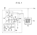
- Fig. 1 is a block diagram of an internal voltage generating circuit having a reference voltage generating circuit of an embodiment of the invention.
- Fig. 2 is a block diagram of an internal voltage generating circuit having a reference voltage generating circuit in the prior art.
- Fig. 3 is a circuit diagram of the reference voltage generating circuit of Fig. 2.
- Fig. 4 is a diagram showing the junction temperature-reference voltage characteristics of the circuit of Fig. 3.
- Fig. 5 is a diagram showing the junction temperature-reference voltage characteristics of the reference voltage generating circuit of Fig. 1.
- Fig. 1 is a block diagram showing an internal voltage generating circuit having a reference voltage generating circuit of an embodiment of the invention.
- the internal voltage generating circuit is configured of CMOS semiconductor integrated circuits, and comprises a reference voltage generating circuit 30 energized from the power supply voltage Vcc to generate a reference voltage (third reference voltage) Vref, and an internal voltage driving circuit 70 which is energized by the power supply voltage Vcc and responsive to the reference voltage Vref, and supplies the internal voltage Vx to the load in the integrated circuit.
- the reference voltage generating circuit 30 comprises a first reference voltage circuit 40 for outputting a reference voltage (first reference voltage) Vin1 and the reference voltage (third reference voltage) Vref for the internal voltage driving circuit 70, a second reference voltage circuit 50 for generating a reference voltage (second reference voltage) Vin2, and a comparator means 60 consisting of a differential amplifier 61 comparing the reference voltages vin1 and Vin2 and feeding back, to the first reference voltage circuit 40, a comparator output signal VA which indicates the result of the comparison.
- the first reference voltage circuit 40 comprises a constant current source 41 which is configured of MOS transistors etc. and which maintains a constant current through it, and PMOS transistors 42 and 43.
- the gate and drain of the PMOS transistor 42 are commonly connected, and the common node N1 is connected to the constant current source 41, and the source of the PMOS transistor 42 is connected to the power supply voltage Vcc through the PMOS transistor 43.
- the PMOS transistor 42 generates the reference voltage Vp, and the reference voltage Vin1 is output from the common node N1.
- the second reference voltage circuit 50 comprises a constant current source 51 which is configured of MOS transistors, etc. and which supplies a constant current through an NMOS transistor 52.
- the gate and the drain of the NMOS transistor 52 are commonly connected, and the common node N2 is connected to the constant current source 51, and the source of the NMOS transistor 52 connected to the reference potential GND.
- the reference voltage Vin2 is output from the common node N2.
- the reference voltage Vin2 is equal to the reference voltage Vn generated at the NMOS transistor 52.
- the differential amplifier 61 constituting the comparator means 60 have its non-inverting input terminal (+) connected to the common node N1 and its inverting input terminal (-) connected to the common node N2, and the output terminal of the differential amplifier 61 for producing a comparator output signal VA is connected to the gate of the PMOS transistor 43 in the first reference voltage circuit 40 for feedback.
- the reference voltage Vref is output from the drain of the PMOS transistor 43, and supplied to the internal voltage driving circuit 70.
- the internal voltage driving circuit 70 comprises a differential amplifier operating in response to the difference between the reference voltage Vref and the voltage feed back from the internal voltage Vx, and an output buffer for outputting the internal voltage Vx which can drive a large capacity, large current load.
- Fig. 5 is a junction temperature-reference voltage characteristics diagram of the reference voltage generating circuit 30 shown in Fig. 1. The operation of the circuit of Fig. 1 will now be described with reference to Fig. 5.
- the PMOS transistor 43 When the output of the differential amplifier 61 is Low, the PMOS transistor 43 is turned on. Accordingly, the stable reference voltage Vref is output from the drain of the PMOS transistor 43, and applied to the internal voltage driving circuit 70.
- the internal voltage driving circuit 70 is responsive to the reference voltage Vref and supplies the internal voltage Vx to power the load in the semiconductor integrated circuit.
- the temperature characteristics of the reference voltage Vn accompanying the increase in the junction temperature of the NMOS transistor 52 is either of the following two types depending on how the channel length, the channel width and other parameters are selected. That is, the NMOS transistor 52 (this also applies to a PMOS transistor) has its threshold value decreased and its mutual conductance g m decreased when the junction temperature is increased. Accordingly, the types of the temperature characteristics are as follows:
- the type (2) is selected for the reference Vn, and the reference voltage Vn increases with temperature increase.
- the reference voltage Vp can have either of the two type of the temperature characteristics. It is assumed that the reference voltage Vp increases, like the NMOS transistor 42.
- Vin1 approximately equals Vin2
- Vref approximately equals Vn + Vp Since Vn > 0, and Vp > 0 when the junction temperature increases, the reference voltage is always positive.
- the set value of the reference voltage Vref is represented by the sum (Vn + Vp) for any parameters of the PMOS transistor and NMOS transistor, so the manufacturing variations in the fabrication process of the PMOS transistor and NMOS transistor can be expressed by the reference voltage Vref. Accordingly, by appropriately selecting the parameters of the PMOS transistor and the NMOS transistor, the temperature characteristics shown in Fig. 5 is obtained by computer simulation. The temperature characteristics is of the positive gradient which is opposite to that of Fig. 4, and the reference voltage Vref increases with the junction temperature.
- the first and the second reference voltages are generated from the first and the second reference voltage circuit, and are compared at the comparator means, and the output of the comparator means is fed back to the first reference voltage circuit to produce the third reference voltage.
- the third reference voltage is therefore determined in accordance with both of the MOS transistor having the first channel type and the MOS transistor having the second channel type. The manufacturing variations in the fabrication process of either of the transistors can be compensated, and a stable reference voltage can be output.
- the temperature dependence of the third reference voltage can be made to be positive, so that the third voltage increases with the temperature increase, and the delay in the operation of the circuit driven by the third reference voltage can be prevented.
- the reference voltage generating circuit is formed using the forward voltage drop of a diode which is not dependent on the power supply voltage fluctuations, special fabrication steps for a diode or the like need not be added in the fabrication process of the semiconductor integrated circuit, so the fabrication process of the semiconductor integrated circuit can be simplified and the cost can be lowered.
Landscapes
- Engineering & Computer Science (AREA)
- Physics & Mathematics (AREA)
- Microelectronics & Electronic Packaging (AREA)
- Electromagnetism (AREA)
- General Physics & Mathematics (AREA)
- Radar, Positioning & Navigation (AREA)
- Automation & Control Theory (AREA)
- Nonlinear Science (AREA)
- Control Of Electrical Variables (AREA)
- Dram (AREA)
- Logic Circuits (AREA)
- Semiconductor Integrated Circuits (AREA)
Applications Claiming Priority (2)
| Application Number | Priority Date | Filing Date | Title |
|---|---|---|---|
| JP2098483A JPH03296118A (ja) | 1990-04-13 | 1990-04-13 | 基準電圧発生回路 |
| JP98483/90 | 1990-04-13 |
Publications (3)
| Publication Number | Publication Date |
|---|---|
| EP0451870A2 true EP0451870A2 (fr) | 1991-10-16 |
| EP0451870A3 EP0451870A3 (en) | 1992-04-01 |
| EP0451870B1 EP0451870B1 (fr) | 1995-08-09 |
Family
ID=14220898
Family Applications (1)
| Application Number | Title | Priority Date | Filing Date |
|---|---|---|---|
| EP91105890A Expired - Lifetime EP0451870B1 (fr) | 1990-04-13 | 1991-04-12 | Circuit de génération d'une tension de référence |
Country Status (5)
| Country | Link |
|---|---|
| US (1) | US5103158A (fr) |
| EP (1) | EP0451870B1 (fr) |
| JP (1) | JPH03296118A (fr) |
| KR (1) | KR0126911B1 (fr) |
| DE (1) | DE69111869T2 (fr) |
Cited By (1)
| Publication number | Priority date | Publication date | Assignee | Title |
|---|---|---|---|---|
| EP0944159A3 (fr) * | 1998-03-20 | 2003-05-28 | Micronas GmbH | Convertisseur de courant continu |
Families Citing this family (15)
| Publication number | Priority date | Publication date | Assignee | Title |
|---|---|---|---|---|
| KR950008453B1 (ko) * | 1992-03-31 | 1995-07-31 | 삼성전자주식회사 | 내부전원전압 발생회로 |
| EP0576774B1 (fr) * | 1992-06-30 | 1999-09-15 | STMicroelectronics S.r.l. | Régulateur de tension pour dispositifs de mémoire |
| JP2851767B2 (ja) * | 1992-10-15 | 1999-01-27 | 三菱電機株式会社 | 電圧供給回路および内部降圧回路 |
| IT1272933B (it) * | 1994-01-28 | 1997-07-01 | Fujitsu Ltd | Dispositivo a circuito integrato di semiconduttore |
| US5748035A (en) * | 1994-05-27 | 1998-05-05 | Arithmos, Inc. | Channel coupled feedback circuits |
| US5748030A (en) * | 1996-08-19 | 1998-05-05 | Motorola, Inc. | Bias generator providing process and temperature invariant MOSFET transconductance |
| JPH10133754A (ja) * | 1996-10-28 | 1998-05-22 | Fujitsu Ltd | レギュレータ回路及び半導体集積回路装置 |
| US6943618B1 (en) * | 1999-05-13 | 2005-09-13 | Honeywell International Inc. | Compensation mechanism for compensating bias levels of an operation circuit in response to supply voltage changes |
| US6583661B1 (en) | 2000-11-03 | 2003-06-24 | Honeywell Inc. | Compensation mechanism for compensating bias levels of an operation circuit in response to supply voltage changes |
| JP3561716B1 (ja) * | 2003-05-30 | 2004-09-02 | 沖電気工業株式会社 | 定電圧回路 |
| US7420397B2 (en) * | 2004-06-02 | 2008-09-02 | Stmicroelectronics Sa | Low-consumption inhibit circuit with hysteresis |
| JP2009048405A (ja) * | 2007-08-20 | 2009-03-05 | Funai Electric Co Ltd | 通信装置 |
| JP5537272B2 (ja) * | 2010-06-07 | 2014-07-02 | ローム株式会社 | 負荷駆動回路装置及びこれを用いた電気機器 |
| JP7325352B2 (ja) * | 2020-02-07 | 2023-08-14 | エイブリック株式会社 | 基準電圧回路 |
| CN115308467B (zh) * | 2021-05-07 | 2025-12-23 | 脸萌有限公司 | 集成电路内部电压检测电路、检测方法以及集成电路 |
Family Cites Families (9)
| Publication number | Priority date | Publication date | Assignee | Title |
|---|---|---|---|---|
| US3975648A (en) * | 1975-06-16 | 1976-08-17 | Hewlett-Packard Company | Flat-band voltage reference |
| US4357571A (en) * | 1978-09-29 | 1982-11-02 | Siemens Aktiengesellschaft | FET Module with reference source chargeable memory gate |
| CH628462A5 (fr) * | 1978-12-22 | 1982-02-26 | Centre Electron Horloger | Source de tension de reference. |
| US4346344A (en) * | 1979-02-08 | 1982-08-24 | Signetics Corporation | Stable field effect transistor voltage reference |
| JP2525346B2 (ja) * | 1983-10-27 | 1996-08-21 | 富士通株式会社 | 定電流源回路を有する差動増幅回路 |
| JPH0668706B2 (ja) * | 1984-08-10 | 1994-08-31 | 日本電気株式会社 | 基準電圧発生回路 |
| US4588941A (en) * | 1985-02-11 | 1986-05-13 | At&T Bell Laboratories | Cascode CMOS bandgap reference |
| US4837459A (en) * | 1987-07-13 | 1989-06-06 | International Business Machines Corp. | CMOS reference voltage generation |
| US4868482A (en) * | 1987-10-05 | 1989-09-19 | Western Digital Corporation | CMOS integrated circuit having precision resistor elements |
-
1990
- 1990-04-13 JP JP2098483A patent/JPH03296118A/ja active Pending
-
1991
- 1991-03-13 KR KR1019910004007A patent/KR0126911B1/ko not_active Expired - Fee Related
- 1991-04-08 US US07/682,189 patent/US5103158A/en not_active Expired - Lifetime
- 1991-04-12 EP EP91105890A patent/EP0451870B1/fr not_active Expired - Lifetime
- 1991-04-12 DE DE69111869T patent/DE69111869T2/de not_active Expired - Lifetime
Cited By (1)
| Publication number | Priority date | Publication date | Assignee | Title |
|---|---|---|---|---|
| EP0944159A3 (fr) * | 1998-03-20 | 2003-05-28 | Micronas GmbH | Convertisseur de courant continu |
Also Published As
| Publication number | Publication date |
|---|---|
| KR910019310A (ko) | 1991-11-30 |
| KR0126911B1 (ko) | 1998-10-01 |
| DE69111869D1 (de) | 1995-09-14 |
| DE69111869T2 (de) | 1996-05-02 |
| EP0451870A3 (en) | 1992-04-01 |
| US5103158A (en) | 1992-04-07 |
| JPH03296118A (ja) | 1991-12-26 |
| EP0451870B1 (fr) | 1995-08-09 |
Similar Documents
| Publication | Publication Date | Title |
|---|---|---|
| US5982162A (en) | Internal voltage generation circuit that down-converts external power supply voltage and semiconductor device generating internal power supply voltage on the basis of reference voltage | |
| US6225855B1 (en) | Reference voltage generation circuit using source followers | |
| US4634894A (en) | Low power CMOS reference generator with low impedance driver | |
| US5146152A (en) | Circuit for generating internal supply voltage | |
| EP0451870B1 (fr) | Circuit de génération d'une tension de référence | |
| US5077518A (en) | Source voltage control circuit | |
| US5087834A (en) | Buffer circuit including comparison of voltage-shifted references | |
| JP5074542B2 (ja) | 内部電圧発生回路 | |
| US5532578A (en) | Reference voltage generator utilizing CMOS transistor | |
| EP0535325B1 (fr) | Générateur de tension pour un dispositif de mémoire | |
| US5933051A (en) | Constant-voltage generating device | |
| US4868483A (en) | Power voltage regulator circuit | |
| US5136182A (en) | Controlled voltage or current source, and logic gate with same | |
| KR100218078B1 (ko) | 외부전원전압의 변동이나 환경온도의 변화에 대한 출력전압의 변동을 억제할 수 있는 기판전위발생회로 | |
| US7764114B2 (en) | Voltage divider and internal supply voltage generation circuit including the same | |
| US5886567A (en) | Back bias voltage level detector | |
| US6201436B1 (en) | Bias current generating circuits and methods for integrated circuits including bias current generators that increase and decrease with temperature | |
| US5212440A (en) | Quick response CMOS voltage reference circuit | |
| KR100401392B1 (ko) | 전압조절회로및그방법,조절된전압조절회로및메모리회로 | |
| US6400207B1 (en) | Quick turn-on disable/enable bias control circuit for high speed CMOS opamp | |
| CN1672110A (zh) | 带隙参考电路 | |
| US5221864A (en) | Stable voltage reference circuit with high Vt devices | |
| US4855624A (en) | Low-power bipolar-CMOS interface circuit | |
| JPH06169240A (ja) | 半導体集積回路 | |
| KR20000004505A (ko) | 내부 전압 강하 회로 |
Legal Events
| Date | Code | Title | Description |
|---|---|---|---|
| PUAI | Public reference made under article 153(3) epc to a published international application that has entered the european phase |
Free format text: ORIGINAL CODE: 0009012 |
|
| AK | Designated contracting states |
Kind code of ref document: A2 Designated state(s): DE FR NL |
|
| PUAL | Search report despatched |
Free format text: ORIGINAL CODE: 0009013 |
|
| AK | Designated contracting states |
Kind code of ref document: A3 Designated state(s): DE FR NL |
|
| 17P | Request for examination filed |
Effective date: 19920430 |
|
| 17Q | First examination report despatched |
Effective date: 19940318 |
|
| GRAA | (expected) grant |
Free format text: ORIGINAL CODE: 0009210 |
|
| AK | Designated contracting states |
Kind code of ref document: B1 Designated state(s): DE FR NL |
|
| ET | Fr: translation filed | ||
| REF | Corresponds to: |
Ref document number: 69111869 Country of ref document: DE Date of ref document: 19950914 |
|
| PLBE | No opposition filed within time limit |
Free format text: ORIGINAL CODE: 0009261 |
|
| STAA | Information on the status of an ep patent application or granted ep patent |
Free format text: STATUS: NO OPPOSITION FILED WITHIN TIME LIMIT |
|
| 26N | No opposition filed | ||
| PGFP | Annual fee paid to national office [announced via postgrant information from national office to epo] |
Ref country code: FR Payment date: 20100521 Year of fee payment: 20 |
|
| PGFP | Annual fee paid to national office [announced via postgrant information from national office to epo] |
Ref country code: DE Payment date: 20100430 Year of fee payment: 20 Ref country code: NL Payment date: 20100416 Year of fee payment: 20 |
|
| REG | Reference to a national code |
Ref country code: DE Ref legal event code: R071 Ref document number: 69111869 Country of ref document: DE |
|
| REG | Reference to a national code |
Ref country code: NL Ref legal event code: V4 Effective date: 20110412 |
|
| PG25 | Lapsed in a contracting state [announced via postgrant information from national office to epo] |
Ref country code: NL Free format text: LAPSE BECAUSE OF EXPIRATION OF PROTECTION Effective date: 20110412 |
|
| PG25 | Lapsed in a contracting state [announced via postgrant information from national office to epo] |
Ref country code: DE Free format text: LAPSE BECAUSE OF EXPIRATION OF PROTECTION Effective date: 20110412 |