EP0452064A2 - Apparatus for detecting digital data - Google Patents
Apparatus for detecting digital data Download PDFInfo
- Publication number
- EP0452064A2 EP0452064A2 EP91303071A EP91303071A EP0452064A2 EP 0452064 A2 EP0452064 A2 EP 0452064A2 EP 91303071 A EP91303071 A EP 91303071A EP 91303071 A EP91303071 A EP 91303071A EP 0452064 A2 EP0452064 A2 EP 0452064A2
- Authority
- EP
- European Patent Office
- Prior art keywords
- digital data
- channels
- data
- distributing
- processing
- Prior art date
- Legal status (The legal status is an assumption and is not a legal conclusion. Google has not performed a legal analysis and makes no representation as to the accuracy of the status listed.)
- Granted
Links
Images



Classifications
-
- H—ELECTRICITY
- H04—ELECTRIC COMMUNICATION TECHNIQUE
- H04N—PICTORIAL COMMUNICATION, e.g. TELEVISION
- H04N5/00—Details of television systems
- H04N5/76—Television signal recording
- H04N5/91—Television signal processing therefor
- H04N5/92—Transformation of the television signal for recording, e.g. modulation, frequency changing; Inverse transformation for playback
- H04N5/926—Transformation of the television signal for recording, e.g. modulation, frequency changing; Inverse transformation for playback by pulse code modulation
-
- G—PHYSICS
- G11—INFORMATION STORAGE
- G11B—INFORMATION STORAGE BASED ON RELATIVE MOVEMENT BETWEEN RECORD CARRIER AND TRANSDUCER
- G11B20/00—Signal processing not specific to the method of recording or reproducing; Circuits therefor
- G11B20/10—Digital recording or reproducing
- G11B20/10009—Improvement or modification of read or write signals
-
- H—ELECTRICITY
- H04—ELECTRIC COMMUNICATION TECHNIQUE
- H04N—PICTORIAL COMMUNICATION, e.g. TELEVISION
- H04N5/00—Details of television systems
- H04N5/76—Television signal recording
- H04N5/91—Television signal processing therefor
- H04N5/93—Regeneration of the television signal or of selected parts thereof
- H04N5/931—Regeneration of the television signal or of selected parts thereof for restoring the level of the reproduced signal
Definitions
- This invention relates to apparatus for detecting digital data, and more particularly but not exclusively, is directed to apparatus for detecting digital data for use in a video tape recorder which uses class IV or other partial response signalling in high density digital tape recording and reproducing.
- VTRs Digital video tape recorders
- the electromagnetic transducing system used therefor (such as a magnetic head or the like) has a differentiation characteristic so that the carrier-to-noise (C/N) ratio is degraded at lower frequencies.
- the C/N ratio will be similarly degraded due to a magnetisation characteristic of the magnetic tape itself, as shown in Figure 1 of the accompanying drawings, if the frequency is increased.
- a magnetic recording and/or reproducing system for a digitised video signal (hereinafter referred to as a digital video signal)
- the frequency band in which a satisfactory C/N ratio can be obtained is relatively narrow.
- a detection system is employed having a signal spectrum concentrated near a region in which the C/N ratio is maximised, so as to effectively avoid deterioration of the C/N ratio of the reproduced signal, and thereby ensure that the digital video signal will be recorded and/or reproduced efficiently.
- it has been proposed to utilise a class IV partial response scheme in the reproduction and detection of a digital video signal for example, as disclosed in US Patent Nos. US-A-4 504 872 and US-A-4 984 099 both assigned to the present applicants.
- the digital video signal can be recorded and/or reproduced efficiently by effectively utilising the frequency characteristic of the magnetic recording and/or reproducing system.
- the electromagnetic transducing system for example, a magnetic head
- a reproduced signal from the magnetic head has a characteristic expressed as (1 - D) with reference to the delay operator D and which is shown by the correspondingly labelled dashed line in Figure 2.
- a digital video signal having a low bit error rate can be reproduced by the application of the Viterbi decoding technique, which indicates that, as shown in Figure 2, the digital video signal can be efficiently detected by effectively utilising a frequency characteristic nearly equal to the characteristic of Figure 1 which represents the frequency characteristic of the magnetic recording and/or reproducing system.
- a Viterbi decoding circuit utilises the likelihood of correlation between data input successively thereto for detecting transit of the data, and decodes the data on the basis of the detected result.
- the bit error rate of the decoded data can be reduced as compared with a standard decoding circuit which decodes data with reference to the signal level.
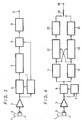
- a previously-proposed reproducing circuit of a digital VTR which incorporates class IV partial response and Viterbi decoding schemes will now be described with reference to Figure 3 of the accompanying drawings in which digital video data recorded as a binary signal in analog form on a video tape 1 is reproduced by a magnetic head 2.
- the reproduced signal is supplied through an amplifier 3 to an equaliser circuit 4, and the equalised reproduced signal from the equaliser circuit 4 is supplied to a processing circuit 5.
- the processing circuit 5 performs on this reproduced signal the calculation (1 + D) in accordance with the above-mentioned partial response scheme.
- the resulting output of the processing circuit 5 is supplied to an analog-to-digital (A/D) converter 6.
- a reproduced clock is generated from the reproduced signal by a phase-locked loop (PLL) circuit 7 also connected to the output of the amplifier 3.
- PLL phase-locked loop
- This reproduced clock is supplied to the A/D converter 6 which detects digital data from the reproduced signal level on the basis of the reproduced clock.
- Detected digital data is supplied to a Viterbi decoder circuit 8, in which the data is decoded in accordance with the Viterbi decoding scheme to provide a detected digital video signal.
- the detected digital video signal is supplied through an output terminal 9 to a reproduced signal processor circuit (not shown) in a succeeding stage.
- the transmission rate of the digital video data is very high so that the clock frequency necessary for processing reproduced data in each of the circuits must be selected to be higher than about 30 MHz.
- the circuits which are operated at such a high clock frequency require a calculation circuit of a special configuration, which cannot be readily provided in practice.
- the equaliser circuit 4 and the processing circuit 5 be fabricated as digital circuits because such digital equaliser circuits and digital processing circuits can provide excellent characteristics.
- apparatus for detecting input digital data comprising: distributing means for distributing said input digital data into at least two channels; processing means in each of said channels for processing said digital data in the respective channel in accordance with a predetermined formula; decoder means in each of said channels for decoding an output of said processing means in said respective channel in accordance with the Viterbi algorithm; and means for composing outputs of said decoder means in said channels to obtain digital data in one sequence.
- apparatus for detecting digital data from a binary signal recorded in analog form on a magnetic medium
- the apparatus comprising: playback means including a magnetic head for reproducing said signal recorded on said magnetic medium; analog-to-digital converter means for converting an output of said playback means into digital data; distributing means for distributing said digital data from said converter means into at least two channels; processing means in each of said channels for processing said digital data in the respective one of said channels in accordance with a class IV partial response; decoder means in each of said channels for decoding an output of said processing means in the respective channel in accordance with the Viterbi algorithm; and means for composing the outputs of said decoder means in said channels to obtain digital data in one sequence.
- a preferred embodiment of the invention provides an improved apparatus for detecting digital data in which the above-mentioned problems and disadvantages encountered with the previously-proposed systems can be substantially overcome.
- the signal processing speed of each of the circuits can be substantially reduced.
- the circuit arrangement can be simplified so as to be operable by a clock signal of a relatively low frequency.
- the invention is applied to a reproducing system of a digital video tape recorder (VTR) in which digital data representing a video signal are recorded as a binary signal in analog form on a magnetic tape.
- VTR digital video tape recorder
- This reproducing system is generally arranged as shown in Figure 4, in which the signal reproduced from the magnetic tape 1 by the magnetic head 2 is supplied through the playback amplifier 3 to the A/D converter 6, and digital data is derived from the reproduced signal by the A/D converter 6 on the basis of the reproduced clock signal supplied thereto from the PLL circuit 7.
- Digital data output from the A/D converter 6 are divided into an odd sequence and an even sequence which are then supplied to respective channels containing equaliser circuits 11 and 12.
- each of the equaliser circuits 11 and 12 is formed by a transversal filter.
- Outputs of the equaliser circuits 11 and 12 are supplied to processing circuits 21 and 22 in the respective channels, which perform the (1 + D) calculation on the outputs of the equaliser circuits 11 and 12, respectively, where D is a delay operator.
- the processing circuit 21 derives the resulting processed data for the odd sequence and the processing circuit 22 derives the resulting processed data for the even sequence.
- Outputs of the processing circuits 21 and 22 are supplied to Viterbi decoders 23 and 24, in the respective channels.
- the Viterbi decoder 23 is operable to Viterbi-decode data of the odd sequence and the Viterbi decoder 24 is operable to Viterbi-decode data of the even sequence.
- Outputs of the two Viterbi decoders 23 and 24 are supplied to a change-over or composing switch 25.
- the change-over switch 25 alternately switches the outputs for the odd sequence and the even sequence from the Viterbi decoders 23 and 24 to compose them into data of one sequence, and supplies this data of one sequence to an output terminal 26. Data developed at the output terminal 26 are supplied to a reproduced signal processing circuit (not shown) forming a succeeding stage.
- the A/D converter 6 detects digital data from the level of a reproduced signal developed at a terminal 6a on the basis of a reproduced clock signal supplied thereto through a terminal 6b from the PLL circuit 7 ( Figure 4).
- the frequency of the reproduced clock signal supplied to the terminal 6b is selected to be 40 MHz.
- the output digital data from the A/D converter 6 are supplied to a distributor which includes latch circuits 41 and 42.
- the latch circuits 41 and 42 latch the digital data on the basis of a clock signal having a frequency of 20 MHz and which is supplied thereto through a terminal 40.
- the clock signal supplied to the latch circuit 41 and the clock signal supplied to the latch circuit 42 are inverted in phase relative to each other by 180 degrees, so that the latch timings of the latch circuits 41 and 42 are mutually displaced, whereby data of an even sequence is latched by the latch circuit 41 and data of an odd sequence is latched by the latch circuit 42.
- Data latched by the latch circuit 41 is supplied through a latch circuit 43 functioning as a delay circuit to the equaliser circuits 11 and 12, and data latched by the latch circuit 42 is supplied through latch circuits 44 and 45 arranged in series and also functioning as delay circuits to the equaliser circuits 11 and 12.
- the 20 MHz clock signal applied to the terminal 40 is also supplied to the latch circuits 43, 44 and 45, so that data are delayed by one clock in each of the latch circuits 43, 44 and 45.
- output data from the latch circuit 43 is supplied to a series circuit of delay circuits 11a and 11b and output data from the latch circuit 45 is supplied to a delay circuit 11c. Outputs of the delay circuits 11a, 11b and 11c are supplied through respective coefficient multipliers 11d, 11e and 11f to an adder 11g.
- output data from the latch circuit 43 is supplied to a series circuit of delay circuits 12a and 12b, and output data from the latch circuit 45 is supplied to a series circuit of delay circuits 12c and 12d.
- Outputs of the delay circuits 12b, 12c and 12d are supplied through respective coefficient multipliers 12e, 12f and 12g to an adder 12h.
- the coefficient multipliers 11d, 11e and 11f and the coefficient multipliers 12e, 12f and 12g are operative to multiply the respective delayed data supplied thereto by coefficients K1, K2 and K3, respectively.
- the two equaliser circuits 11 and 12 constitute respective transversal filters and the adders 11g and 12h provide respective equalised signals.
- the equalising level is changed.
- Each of the delay circuits 11a, 11b, 11c, 12a, 12b, 12c and 12d is formed by a latch circuit which delays an input signal by a delay time of one clock having the frequency of 20 MHz.
- Outputs of the equaliser circuits 11 and 12 are supplied to the processing circuit 21 which performs the (1 + D) calculation so as to obtain the processed data of the odd sequence. More specifically, the output data of the equaliser circuit 11 is supplied through a series circuit of delay circuits 21a and 21b to one input terminal of an adder 21c, and the output of the equaliser circuit 12 is supplied through a delay circuit 22a to the other input terminal of the adder 21c. An added or sum output of the adder 21c is supplied through a delay circuit 21d to an input terminal 23a of the Viterbi decoder circuit 23 ( Figure 4) in the respective channel. In other words, the output of the delay circuit 21d is supplied to the Viterbi decoder circuit 23 which Viterbi-decodes the odd sequence data constituting the output of the processing circuit 21.
- the outputs of the equaliser circuits 11 and 12 are also supplied to the processing circuit 22 which performs the (1 + D) calculation so as to obtain the processed data of the even sequence. More specifically, the output of the delay circuit 21a in the odd sequence data processing circuit 21 is supplied to one input terminal of an adder 22b, and an output of the delay circuit 22a is supplied to the other input terminal of the adder 22b. An added or sum output of the adder 22b is supplied through a delay circuit 22c to an input terminal 24a of the Viterbi decoder circuit 24 ( Figure 4). In other words, the output of the delay circuit 22c is supplied to the Viterbi decoder circuit 24 which Viterbi-decodes the even sequence data constituting the output of the processing circuit 22.
- Each of the delay circuits 21a, 21b and 21d, and each of the delay circuits 22a and 22c in the processing circuits 21 and 22 respectively, is formed of a latch circuit which delays the input signal supplied thereto by a delay time of one clock period of the clock signal having a frequency of 20 MHz.
- the separated even sequence data and odd sequence data are then supplied to the respective transversal filter or equaliser circuits 11 and 12, thereby generating equalised data EQ which are separately equalised for the odd and even sequences. More specifically, assuming that data EQ1, EQ3, EQ5, Vietnamese obtained at a junction or point e1 corresponding to the output of the delay circuit 21a, are considered to be the output of the equaliser circuit 11, as shown in Figure 7A, then data EQ0, EQ2, EQ4, Vietnamese are obtained at a point e2, corresponding to the output of the delay circuit 22a at the same timing, and may be considered to be the output of the equaliser circuit 12, as shown in Figure 7B. Further, at the same timing, as shown in Figure 7C, data EQ ⁇ 1, EQ1, EQ3, Vietnamese will be obtained at a point e3 corresponding to the output of the delay circuit 21b.
- the added or sum output of the adder 21c in the processing circuit 21 is simply the sum of the signals at the points e2 and e3, and hence becomes the data EQ ⁇ 1 + EQ0, EQ1 + EQ2, EQ3 + EQ4, ## as shown in Figure 7D.
- This added output is supplied to the Viterbi decoder circuit 23 which decodes the odd sequence data as data processed by (1 + D).
- the added or sum output of the adder 22b in the processing circuit 22 is simply the sum of the signals at the points e1 and e2, and hence becomes the data EQ1 + EQ0, EQ3 + EQ2, EQ5 + EQ4, ## as shown in Figure 7E.
- This added output is supplied to the Viterbi decoder circuit 24 which decodes the even sequence data as data processed by (1 + D).
- the odd sequence and even sequence data are separately decoded by the two Viterbi decoder circuits 23 and 24, and are then composed into data of one sequence by operation of the switch 25.
- the reproduced signal is converted into digital data by the A/D converter 6 before being equalised so that the transversal filter or equaliser circuits 11 and 12 and the processing circuits 21 and 22, each of which performs the calculation of (1 + D), can be fabricated as digital circuits. Accordingly, the digital equaliser circuits 11 and 12 and the digital processing circuits 21 and 22 can be provided with stable characteristics which can be adjusted with ease.
- the equaliser circuits 11 and 12 and the processing circuits 21 and 22 are arranged in respective channels to divide the data into odd sequence data and even sequence data, the digital signal having a sampling frequency of 40 MHz is equalised using a clock frequency which is one-half the sampling frequency, that is, a clock frequency of 20 MHz, and the (1 + D) calculation or processing is also performed at such reduced frequency. Therefore, a simplified digital data detecting circuit which is operable by a clock signal of relatively low frequency can be employed, that is, there is no need to provide a special circuit which is operated by a clock signal of high frequency.
- the reproduced data is divided into data of two channels, that is, odd sequence data and even sequence data in the above described embodiment, it will be appreciated that the reproduced data may be divided into data of three or more channels thereby to further lower the clock frequency.
Landscapes
- Engineering & Computer Science (AREA)
- Signal Processing (AREA)
- Multimedia (AREA)
- Signal Processing For Digital Recording And Reproducing (AREA)
- Error Detection And Correction (AREA)
Abstract
Description
- This invention relates to apparatus for detecting digital data, and more particularly but not exclusively, is directed to apparatus for detecting digital data for use in a video tape recorder which uses class IV or other partial response signalling in high density digital tape recording and reproducing.
- Digital video tape recorders (VTRs) have been developed to record a video signal in the form of a digital signal on a magnetic tape such that deterioration of image quality in the dubbing mode can be minimised.
- When a signal is recorded on and/or reproduced from a magnetic tape, the electromagnetic transducing system used therefor (such as a magnetic head or the like) has a differentiation characteristic so that the carrier-to-noise (C/N) ratio is degraded at lower frequencies. The C/N ratio will be similarly degraded due to a magnetisation characteristic of the magnetic tape itself, as shown in Figure 1 of the accompanying drawings, if the frequency is increased.
- Accordingly, when using a magnetic recording and/or reproducing system for a digitised video signal (hereinafter referred to as a digital video signal), the frequency band in which a satisfactory C/N ratio can be obtained is relatively narrow. For this reason, when a digital video signal is to be detected, a detection system is employed having a signal spectrum concentrated near a region in which the C/N ratio is maximised, so as to effectively avoid deterioration of the C/N ratio of the reproduced signal, and thereby ensure that the digital video signal will be recorded and/or reproduced efficiently. In connection with the foregoing, it has been proposed to utilise a class IV partial response scheme in the reproduction and detection of a digital video signal, for example, as disclosed in US Patent Nos. US-A-4 504 872 and US-A-4 984 099 both assigned to the present applicants.
- More specifically, since the C/N ratio in a magnetic recording and/or reproducing system is degraded at the lower and higher frequencies, its frequency characteristic can be approximated by a frequency characteristic H(ω) of a class IV partial response (1 - D²) scheme expressed by using a delay operator D, as shown in Figure 2 of the accompanying drawings.
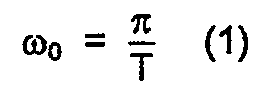
- The Nyquist frequency ω₀ at which the response is minimised has a relation to the delay time T imposed by the delay operator D as expressed in the following equation:
- Accordingly, if the amount of delay imposed by the delay operator D is selected so that the signal spectrum is concentrated near the region in which the C/N ratio is maximised, then the digital video signal can be recorded and/or reproduced efficiently by effectively utilising the frequency characteristic of the magnetic recording and/or reproducing system.
- In other words, in the recording mode, a calculation process corresponding to the following expression (2) is sequentially performed on the digital video signal:

where MOD2 represents the remainder of 2. - Further, since the electromagnetic transducing system (for example, a magnetic head) has a differentiation characteristic, a reproduced signal from the magnetic head has a characteristic expressed as (1 - D) with reference to the delay operator D and which is shown by the correspondingly labelled dashed line in Figure 2.
- Accordingly, in the playback or reproducing mode, a calculation process of (1 + D) is performed on the reproduced signal, whereby the correction expressed by the following equation can be executed:

- When the digital video signal is recorded and/or reproduced by making effective use of class IV partial response signalling, a digital video signal having a low bit error rate can be reproduced by the application of the Viterbi decoding technique, which indicates that, as shown in Figure 2, the digital video signal can be efficiently detected by effectively utilising a frequency characteristic nearly equal to the characteristic of Figure 1 which represents the frequency characteristic of the magnetic recording and/or reproducing system.
- As disclosed in detail, for example, in "Analog Viterbi Decoding for High Speed Digital Satellite Channels", A.S. Acampora et al., IEEE Transactions on Communications, Vol. Com. - 26, No. 10, October 1978, pages 1463-1470, and in "The Viterbi Algorithm", G.D. Forney, Jr., Proceedings of the IEEE, Vol. 61, No. 3, March 1973, pages 268-278, a Viterbi decoding circuit utilises the likelihood of correlation between data input successively thereto for detecting transit of the data, and decodes the data on the basis of the detected result.
- Accordingly, if the relationship (1 - D²) of the reproduced signal relative to the signal used for recording (hereinafter referred to as the recording signal) is utilised to decode the recording signal from the reproduced signal and then the digital video signal is decoded on the basis of the decoded data, the bit error rate of the decoded data can be reduced as compared with a standard decoding circuit which decodes data with reference to the signal level.
- A previously-proposed reproducing circuit of a digital VTR which incorporates class IV partial response and Viterbi decoding schemes will now be described with reference to Figure 3 of the accompanying drawings in which digital video data recorded as a binary signal in analog form on a
video tape 1 is reproduced by amagnetic head 2. The reproduced signal is supplied through anamplifier 3 to anequaliser circuit 4, and the equalised reproduced signal from theequaliser circuit 4 is supplied to aprocessing circuit 5. Theprocessing circuit 5 performs on this reproduced signal the calculation (1 + D) in accordance with the above-mentioned partial response scheme. The resulting output of theprocessing circuit 5 is supplied to an analog-to-digital (A/D)converter 6. A reproduced clock is generated from the reproduced signal by a phase-locked loop (PLL)circuit 7 also connected to the output of theamplifier 3. This reproduced clock is supplied to the A/D converter 6 which detects digital data from the reproduced signal level on the basis of the reproduced clock. Detected digital data is supplied to a Viterbi decoder circuit 8, in which the data is decoded in accordance with the Viterbi decoding scheme to provide a detected digital video signal. The detected digital video signal is supplied through anoutput terminal 9 to a reproduced signal processor circuit (not shown) in a succeeding stage. - When the digital video signal is reproduced by the previously-proposed circuit arrangement of Figure 3, the transmission rate of the digital video data is very high so that the clock frequency necessary for processing reproduced data in each of the circuits must be selected to be higher than about 30 MHz. The circuits which are operated at such a high clock frequency require a calculation circuit of a special configuration, which cannot be readily provided in practice. Further, it is preferable that the
equaliser circuit 4 and theprocessing circuit 5 be fabricated as digital circuits because such digital equaliser circuits and digital processing circuits can provide excellent characteristics. However, it is very difficult to operate theequaliser circuit 4 and theprocessing circuit 5 at any clock frequency higher than about 30 MHz if thesecircuits processing circuits D converter 6 and are not fabricated as digital circuits. - Similarly, in the above US Patent No. US-A-4 504 872, the analog-to-digital conversion follows passage of the reproduced signal through a 1 - D² class IV response filter so that the latter is not fabricated as a digital circuit and, hence, does not provide the advantageous characteristics inherent in digital fabrication.
- According to an aspect of the present invention there is provided apparatus for detecting input digital data, the apparatus comprising:
distributing means for distributing said input digital data into at least two channels;
processing means in each of said channels for processing said digital data in the respective channel in accordance with a predetermined formula;
decoder means in each of said channels for decoding an output of said processing means in said respective channel in accordance with the Viterbi algorithm; and
means for composing outputs of said decoder means in said channels to obtain digital data in one sequence. - In accordance with another aspect of the present invention there is provided apparatus for detecting digital data from a binary signal recorded in analog form on a magnetic medium, the apparatus comprising:
playback means including a magnetic head for reproducing said signal recorded on said magnetic medium;
analog-to-digital converter means for converting an output of said playback means into digital data;
distributing means for distributing said digital data from said converter means into at least two channels;
processing means in each of said channels for processing said digital data in the respective one of said channels in accordance with a class IV partial response;
decoder means in each of said channels for decoding an output of said processing means in the respective channel in accordance with the Viterbi algorithm; and
means for composing the outputs of said decoder means in said channels to obtain digital data in one sequence. - A preferred embodiment of the invention provides an improved apparatus for detecting digital data in which the above-mentioned problems and disadvantages encountered with the previously-proposed systems can be substantially overcome. In the preferred embodiment, when digital data is detected in a digital video tape recorder or the like, the signal processing speed of each of the circuits can be substantially reduced. Also, the circuit arrangement can be simplified so as to be operable by a clock signal of a relatively low frequency.
- The invention will now be described by way of example with reference to the accompanying drawings, throughout which like parts are referred to by like references, and in which:
- Figures 1 and 2 are frequency characteristic graphs to which reference is made in explaining a previously-proposed partial response scheme;
- Figure 3 is a schematic block diagram showing an example of a reproducing circuit of a previously-proposed digital video tape recorder which incorporates a class IV partial response scheme and a Viterbi decoding scheme;
- Figure 4 is a schematic block diagram showing an apparatus for detecting digital data according to an embodiment of the present invention;
- Figure 5 (formed of Figures 5A and 5B) is a schematic block diagram showing a specific example of a main portion of the apparatus shown in Figure 4; and
- Figures 6A to 6C and Figures 7A to 7E are timing charts to which reference is made in explaining the operation of the apparatus shown in Figures 4 and 5.
- An apparatus for detecting digital data according to an embodiment of the present invention will now be described with reference to Figures 4 and 5, in which parts corresponding to those previously described with reference to Figure 3 are identified by the same reference numerals and therefore will not be again described in detail.
- In the preferred embodiment, the invention is applied to a reproducing system of a digital video tape recorder (VTR) in which digital data representing a video signal are recorded as a binary signal in analog form on a magnetic tape. This reproducing system is generally arranged as shown in Figure 4, in which the signal reproduced from the
magnetic tape 1 by themagnetic head 2 is supplied through theplayback amplifier 3 to the A/D converter 6, and digital data is derived from the reproduced signal by the A/D converter 6 on the basis of the reproduced clock signal supplied thereto from thePLL circuit 7. - Digital data output from the A/
D converter 6 are divided into an odd sequence and an even sequence which are then supplied to respective channels containingequaliser circuits equaliser circuits equaliser circuits processing circuits equaliser circuits processing circuit 21 derives the resulting processed data for the odd sequence and theprocessing circuit 22 derives the resulting processed data for the even sequence. - Outputs of the
processing circuits Viterbi decoders Viterbi decoder 23 is operable to Viterbi-decode data of the odd sequence and theViterbi decoder 24 is operable to Viterbi-decode data of the even sequence. Outputs of the twoViterbi decoders switch 25. The change-over switch 25 alternately switches the outputs for the odd sequence and the even sequence from theViterbi decoders output terminal 26. Data developed at theoutput terminal 26 are supplied to a reproduced signal processing circuit (not shown) forming a succeeding stage. - A specific circuit arrangement extending from the A/
D converter 6 through to theprocessing circuits - In the arrangement of Figure 5, the A/
D converter 6 detects digital data from the level of a reproduced signal developed at a terminal 6a on the basis of a reproduced clock signal supplied thereto through a terminal 6b from the PLL circuit 7 (Figure 4). The frequency of the reproduced clock signal supplied to the terminal 6b is selected to be 40 MHz. - The output digital data from the A/
D converter 6 are supplied to a distributor which includeslatch circuits latch circuits latch circuit 41 and the clock signal supplied to thelatch circuit 42 are inverted in phase relative to each other by 180 degrees, so that the latch timings of thelatch circuits latch circuit 41 and data of an odd sequence is latched by thelatch circuit 42. - Data latched by the
latch circuit 41 is supplied through alatch circuit 43 functioning as a delay circuit to theequaliser circuits latch circuit 42 is supplied throughlatch circuits equaliser circuits latch circuits latch circuits - In the
equaliser circuit 11, output data from thelatch circuit 43 is supplied to a series circuit ofdelay circuits latch circuit 45 is supplied to adelay circuit 11c. Outputs of thedelay circuits respective coefficient multipliers adder 11g. In theequaliser circuit 12, output data from thelatch circuit 43 is supplied to a series circuit ofdelay circuits latch circuit 45 is supplied to a series circuit ofdelay circuits delay circuits respective coefficient multipliers adder 12h. Thecoefficient multipliers coefficient multipliers - Thus, the two
equaliser circuits adders coefficient multipliers coefficient multipliers equaliser circuits delay circuits - Outputs of the
equaliser circuits processing circuit 21 which performs the (1 + D) calculation so as to obtain the processed data of the odd sequence. More specifically, the output data of theequaliser circuit 11 is supplied through a series circuit ofdelay circuits adder 21c, and the output of theequaliser circuit 12 is supplied through adelay circuit 22a to the other input terminal of theadder 21c. An added or sum output of theadder 21c is supplied through adelay circuit 21d to aninput terminal 23a of the Viterbi decoder circuit 23 (Figure 4) in the respective channel. In other words, the output of thedelay circuit 21d is supplied to theViterbi decoder circuit 23 which Viterbi-decodes the odd sequence data constituting the output of theprocessing circuit 21. - The outputs of the
equaliser circuits processing circuit 22 which performs the (1 + D) calculation so as to obtain the processed data of the even sequence. More specifically, the output of thedelay circuit 21a in the odd sequencedata processing circuit 21 is supplied to one input terminal of anadder 22b, and an output of thedelay circuit 22a is supplied to the other input terminal of theadder 22b. An added or sum output of theadder 22b is supplied through adelay circuit 22c to aninput terminal 24a of the Viterbi decoder circuit 24 (Figure 4). In other words, the output of thedelay circuit 22c is supplied to theViterbi decoder circuit 24 which Viterbi-decodes the even sequence data constituting the output of theprocessing circuit 22. - Each of the
delay circuits delay circuits processing circuits - Operation of the above embodiment of the invention will now be described with reference to Figures 6A to 6C and Figures 7A to 7E.
- If it is assumed that digital data a₁, a₂, a₃, ..... are output with a sampling frequency of 40 MHz from the A/
D converter 6, as shown in Figure 6A, then such digital data will be divided into data a₀, a₂, a₄ ....., of even sequence (Figure 6B) and data a₋₁, a₁, a₃, ..... of odd sequence (Figure 6C). The data shown in Figure 6B represents the output of thelatch circuit 43 and the data shown in Figure 6C represents the output of thelatch circuit 44. Since the digital data are divided into the even sequence data and the odd sequence data, as described above, the sampling frequency of each of the even or odd sequence data becomes 20 MHz (namely one-half of the sampling frequency of 40 MHz of the original data). Further, by delaying the odd sequence data by means of thelatch circuit 44, the even sequence data and the odd sequence data are synchronised with each other. - The separated even sequence data and odd sequence data are then supplied to the respective transversal filter or
equaliser circuits delay circuit 21a, are considered to be the output of theequaliser circuit 11, as shown in Figure 7A, then data EQ₀, EQ₂, EQ₄, ..... are obtained at a point e₂, corresponding to the output of thedelay circuit 22a at the same timing, and may be considered to be the output of theequaliser circuit 12, as shown in Figure 7B. Further, at the same timing, as shown in Figure 7C, data EQ₋₁, EQ₁, EQ₃, ..... will be obtained at a point e₃ corresponding to the output of thedelay circuit 21b. - The added or sum output of the
adder 21c in theprocessing circuit 21 is simply the sum of the signals at the points e₂ and e₃, and hence becomes the data EQ₋₁ + EQ₀, EQ₁ + EQ₂, EQ₃ + EQ₄, ..... as shown in Figure 7D. This added output is supplied to theViterbi decoder circuit 23 which decodes the odd sequence data as data processed by (1 + D). - Similarly, the added or sum output of the
adder 22b in theprocessing circuit 22 is simply the sum of the signals at the points e₁ and e₂, and hence becomes the data EQ₁ + EQ₀, EQ₃ + EQ₂, EQ₅ + EQ₄, ..... as shown in Figure 7E. This added output is supplied to theViterbi decoder circuit 24 which decodes the even sequence data as data processed by (1 + D). - The odd sequence and even sequence data are separately decoded by the two
Viterbi decoder circuits switch 25. - It will be seen that, in the data detecting circuit according to this embodiment of the invention, the reproduced signal is converted into digital data by the A/
D converter 6 before being equalised so that the transversal filter orequaliser circuits processing circuits digital equaliser circuits digital processing circuits equaliser circuits processing circuits - While the reproduced data is divided into data of two channels, that is, odd sequence data and even sequence data in the above described embodiment, it will be appreciated that the reproduced data may be divided into data of three or more channels thereby to further lower the clock frequency.
- Although the present invention has been described as being applied to the reproducing circuit of a digital VTR, it is not limited thereto and may be applied to other digital devices.
- Since the above described digital data detecting apparatus employing the partial response scheme and the Viterbi decoding system can be incorporated in a simple circuit operated by a clock signal of relatively low frequency, it will be apparent that the digital data detecting apparatus embodying the present invention can be applied to a consumer digital VTR which, of necessity, is limited in cost.
Claims (14)
- Apparatus for detecting input digital data, the apparatus comprising:
distributing means (41,42) for distributing said input digital data into at least two channels;
processing means (21,22) in each of said channels for processing said digital data in the respective channel in accordance with a predetermined formula (1 + D);
decoder means (23,24) in each of said channels for decoding an output of said processing means (21,22) in said respective channel in accordance with the Viterbi algorithm; and
means (25) for composing outputs of said decoder means (23,24) in said channels to obtain digital data in one sequence. - Apparatus according to claim 1, wherein said predetermined formula (1 + D) is derived from a partial response detection scheme.
- Apparatus according to claim 2, wherein said partial response detection scheme is a class IV partial response.
- Apparatus according to claim 1, claim 2 or claim 3, comprising means (6,7) deriving said input digital data from a binary signal of analog form reproduced from a magnetic medium (1) by a magnetic head (2), and wherein said predetermined formula is [1 + D] in which D is a delay operator.
- Apparatus according to any one of the preceding claims, wherein said distributing means (41,42) is operable to distribute said input digital data into said channels number-by-number in a repeated cycle.
- Apparatus according to claim 5, wherein said distributing means (41,42) is operable to distribute odd numbers of said input digital data into one of said channels and even numbers of said input digital data into another of said channels.
- Apparatus according to claim 6 as dependent on claims 4 and 5, wherein said means deriving said input digital data from said reproduced binary signal of analog form includes analog-to-digital converting means (6) having a predetermined sampling frequency, and wherein said distributing means includes first and second latch means (41,42) receiving said input digital data from said converting means (6), means (40) providing a latching signal to said first latch means (41) with a frequency which is one-half said sampling frequency, means inverting said latching signal and applying the inverted latching signal to said second latch means (42) so that said first and second latch means (41,42) are operable to latch odd and even numbered sequences, respectively, of said input digital data, and third latch means (44) in series with said second latch means (42) and also receiving said latching signal for synchronising sequences of digital data applied through said first and third latch means (41,44) to said one channel and to said other channel.
- Apparatus according to any one of claims 1 to 6, comprising means (2,3) for reproducing a binary signal recorded in analog form on a magnetic medium (1), and analog-to-digital converting means (6) for deriving said input digital data from the reproduced binary signal in analog form in advance of said distributing means (41,42).
- Apparatus according to any one of the preceding claims, comprising equaliser means (11,12) constituting a transversal filter in each of said channels between said distributing means (41,42) and the processing means (21,22) in the respective channel.
- Apparatus according to claim 9 as dependent on claim 7 or claim 8, wherein said analog-to-digital converting means (6) has a predetermined sampling frequency, and wherein said equaliser means (11,12) and said processing means (21,22) in each of said channels is operable by a clock having a frequency which is a fraction of said sampling frequency.
- Apparatus for detecting digital data from a binary signal recorded in analog form on a magnetic medium (1), the apparatus comprising:
playback means (2,3) including a magnetic head (2) for reproducing said signal recorded on said magnetic medium (1);
analog-to-digital converter means (6) for converting an output of said playback means (2,3) into digital data;
distributing means (41,42) for distributing said digital data from said converter means (6) into at least two channels;
processing means (21,22) in each of said channels for processing said digital data in the respective one of said channels in accordance with a class IV partial response;
decoder means (23,24) in each of said channels for decoding an output of said processing means (21,22) in the respective channel in accordance with the Viterbi algorithm; and
means (25) for composing the outputs of said decoder means (23,24) in said channels to obtain digital data in one sequence. - Apparatus according to claim 11, wherein said distributing means (41,42) is operable to distribute odd numbers of said digital data from said converter means (6) into one of said channels and even numbers of said digital data from said converter means (6) into another of said channels.
- Apparatus according to claim 11 or claim 12, comprising equaliser means (11,12) functioning as a transversal filter in each of said channels between said distributing means (41,42) and the processing means ( 21, 22 ) in the respective channel.
- Apparatus according to claim 13, wherein said analog-to-digital converter means (6) has a predetermined sampling frequency, and wherein said equaliser means (11,12) and said processing means (21,22) in each of said channels is operable by a clock having a frequency which is one-half of said sampling frequency.
Applications Claiming Priority (2)
| Application Number | Priority Date | Filing Date | Title |
|---|---|---|---|
| JP2095653A JP2830352B2 (en) | 1990-04-11 | 1990-04-11 | Digital data detection device |
| JP95653/90 | 1990-04-11 |
Publications (3)
| Publication Number | Publication Date |
|---|---|
| EP0452064A2 true EP0452064A2 (en) | 1991-10-16 |
| EP0452064A3 EP0452064A3 (en) | 1993-11-24 |
| EP0452064B1 EP0452064B1 (en) | 1996-12-27 |
Family
ID=14143462
Family Applications (1)
| Application Number | Title | Priority Date | Filing Date |
|---|---|---|---|
| EP91303071A Expired - Lifetime EP0452064B1 (en) | 1990-04-11 | 1991-04-08 | Apparatus for detecting digital data |
Country Status (6)
| Country | Link |
|---|---|
| US (1) | US5255128A (en) |
| EP (1) | EP0452064B1 (en) |
| JP (1) | JP2830352B2 (en) |
| KR (1) | KR100221891B1 (en) |
| AU (1) | AU647097B2 (en) |
| DE (1) | DE69123777T2 (en) |
Cited By (2)
| Publication number | Priority date | Publication date | Assignee | Title |
|---|---|---|---|---|
| EP0595454A3 (en) * | 1992-08-27 | 1994-06-15 | Quantum Corp | Disk drive using prml class iv sampling data detection with digital adaptive equalization |
| WO1995015551A1 (en) * | 1993-12-04 | 1995-06-08 | Hewlett-Packard Limited | Retrieving data recorded at different bit densities |
Families Citing this family (13)
| Publication number | Priority date | Publication date | Assignee | Title |
|---|---|---|---|---|
| JPH05234273A (en) * | 1990-11-30 | 1993-09-10 | Hitachi Ltd | Device for evaluating signal waveform and magnetic disk device |
| JPH05234279A (en) * | 1992-02-24 | 1993-09-10 | Sony Corp | Maximum likelihood decoding device and reproduced data demodulating device using the same |
| JP3088844B2 (en) * | 1992-06-03 | 2000-09-18 | パイオニア株式会社 | Digital signal reproduction device |
| DE69321066T2 (en) * | 1992-10-14 | 1999-03-18 | Sony Corp., Tokio/Tokyo | Magnetic disk device |
| JP3456592B2 (en) * | 1993-05-11 | 2003-10-14 | ソニー株式会社 | Optical disk device |
| US5521767A (en) * | 1993-09-17 | 1996-05-28 | Quantum Corporation | Optimized equalizer system for data recovery and timing extraction in partial response read channels |
| JP3347468B2 (en) * | 1994-04-20 | 2002-11-20 | キヤノン株式会社 | Information playback device |
| EP0684605B1 (en) * | 1994-05-23 | 1999-10-06 | STMicroelectronics S.r.l. | Parallel architecture PRML device for processing signals from a magnetic head during a reading step of data stored on a magnetic support |
| EP0684608B1 (en) * | 1994-05-23 | 1999-10-06 | STMicroelectronics S.r.l. | Device for processing servo signals in a parallel architecture PRML reading apparatus for hard disks |
| US5657013A (en) * | 1994-05-25 | 1997-08-12 | Sony Corporation | Data recording apparatus |
| US5774290A (en) * | 1994-08-09 | 1998-06-30 | Canon Kabushiki Kaisha | Reproducing apparatus for varying clock frequencies based upon azimuth angles of a plurality of heads |
| JPH08329619A (en) * | 1994-10-27 | 1996-12-13 | Hitachi Ltd | Data reproducing method, data reproducing device, and data reproducing circuit |
| US7177353B2 (en) * | 2000-03-10 | 2007-02-13 | Broadcom Corporation | Architecture for very high-speed decision feedback sequence estimation |
Family Cites Families (4)
| Publication number | Priority date | Publication date | Assignee | Title |
|---|---|---|---|---|
| US4517610A (en) * | 1982-12-09 | 1985-05-14 | Magnetic Peripherals Inc. | Multichannel signal recovery circuit |
| US4979052A (en) * | 1987-09-29 | 1990-12-18 | Matsushita Electric Industrial Co., Ltd. | Digital signal magnetic recording/reproducing apparatus |
| JP2840747B2 (en) * | 1988-05-25 | 1998-12-24 | ソニー株式会社 | Digital signal reproduction device |
| NL9002772A (en) * | 1990-09-21 | 1992-04-16 | Philips Nv | DEVICE FOR RECORDING A DIGITAL INFORMATION SIGNAL IN A RECORD CARRIER. |
-
1990
- 1990-04-11 JP JP2095653A patent/JP2830352B2/en not_active Expired - Fee Related
-
1991
- 1991-04-04 US US07/680,361 patent/US5255128A/en not_active Expired - Lifetime
- 1991-04-08 EP EP91303071A patent/EP0452064B1/en not_active Expired - Lifetime
- 1991-04-08 DE DE69123777T patent/DE69123777T2/en not_active Expired - Fee Related
- 1991-04-10 AU AU74326/91A patent/AU647097B2/en not_active Ceased
- 1991-04-11 KR KR1019910005754A patent/KR100221891B1/en not_active Expired - Fee Related
Cited By (3)
| Publication number | Priority date | Publication date | Assignee | Title |
|---|---|---|---|---|
| EP0595454A3 (en) * | 1992-08-27 | 1994-06-15 | Quantum Corp | Disk drive using prml class iv sampling data detection with digital adaptive equalization |
| WO1995015551A1 (en) * | 1993-12-04 | 1995-06-08 | Hewlett-Packard Limited | Retrieving data recorded at different bit densities |
| EP0731968A1 (en) * | 1993-12-04 | 1996-09-18 | Hewlett-Packard Limited | Retrieving data recorded at different bit densities |
Also Published As
| Publication number | Publication date |
|---|---|
| JPH03293819A (en) | 1991-12-25 |
| JP2830352B2 (en) | 1998-12-02 |
| AU7432691A (en) | 1991-10-17 |
| US5255128A (en) | 1993-10-19 |
| EP0452064B1 (en) | 1996-12-27 |
| EP0452064A3 (en) | 1993-11-24 |
| DE69123777D1 (en) | 1997-02-06 |
| AU647097B2 (en) | 1994-03-17 |
| KR100221891B1 (en) | 1999-09-15 |
| DE69123777T2 (en) | 1997-04-17 |
Similar Documents
| Publication | Publication Date | Title |
|---|---|---|
| EP0452064B1 (en) | Apparatus for detecting digital data | |
| US5497239A (en) | Digital video signal recording/reproducing apparatus having multiple recording and reproducing paths | |
| US6307900B1 (en) | Method and apparatus for recovering digital data by employing asynchronous data sampling techniques | |
| JPH0793584B2 (en) | Encoder | |
| GB2113946A (en) | Combined data rate reduction system | |
| US5142377A (en) | Time base correction apparatus | |
| EP0385867B1 (en) | Digital signal reproducing apparatus | |
| US5381274A (en) | Apparatus and method for recycling and reproducing a digital video signal | |
| US5377014A (en) | Apparatus and method for displaying recorded compressed digital high definition video information | |
| EP0343929B1 (en) | Digital signal decoding apparatus | |
| HK1002246B (en) | Video signal processing and video stores | |
| HK1002246A1 (en) | Video signal processing and video stores | |
| US4851934A (en) | Analog signal synthesizing processing circuit with periodic noise compensation | |
| US5359469A (en) | Information data recording apparatus | |
| EP0438293B1 (en) | Video signal recording/reproduction device having dropout compensation function | |
| JP2822264B2 (en) | Automatic gain control circuit | |
| JP2708196B2 (en) | Multiple subsampling signal adapter device | |
| JP3059394B2 (en) | Recording and playback device | |
| US6256450B1 (en) | Progressive scanned signal processing apparatus | |
| JP4296652B2 (en) | Digital signal recording device | |
| JP2725382B2 (en) | VTR color signal noise eliminator | |
| JP3319287B2 (en) | Precoder | |
| JPS6126381A (en) | recording device | |
| JP3158373B2 (en) | Magnetic playback device | |
| JPH0793909A (en) | Phase detection circuit |
Legal Events
| Date | Code | Title | Description |
|---|---|---|---|
| PUAI | Public reference made under article 153(3) epc to a published international application that has entered the european phase |
Free format text: ORIGINAL CODE: 0009012 |
|
| AK | Designated contracting states |
Kind code of ref document: A2 Designated state(s): DE FR GB NL |
|
| PUAL | Search report despatched |
Free format text: ORIGINAL CODE: 0009013 |
|
| AK | Designated contracting states |
Kind code of ref document: A3 Designated state(s): DE FR GB NL |
|
| 17P | Request for examination filed |
Effective date: 19940418 |
|
| 17Q | First examination report despatched |
Effective date: 19950109 |
|
| GRAG | Despatch of communication of intention to grant |
Free format text: ORIGINAL CODE: EPIDOS AGRA |
|
| GRAH | Despatch of communication of intention to grant a patent |
Free format text: ORIGINAL CODE: EPIDOS IGRA |
|
| GRAH | Despatch of communication of intention to grant a patent |
Free format text: ORIGINAL CODE: EPIDOS IGRA |
|
| GRAA | (expected) grant |
Free format text: ORIGINAL CODE: 0009210 |
|
| AK | Designated contracting states |
Kind code of ref document: B1 Designated state(s): DE FR GB NL |
|
| REF | Corresponds to: |
Ref document number: 69123777 Country of ref document: DE Date of ref document: 19970206 |
|
| ET | Fr: translation filed | ||
| PLBE | No opposition filed within time limit |
Free format text: ORIGINAL CODE: 0009261 |
|
| STAA | Information on the status of an ep patent application or granted ep patent |
Free format text: STATUS: NO OPPOSITION FILED WITHIN TIME LIMIT |
|
| 26N | No opposition filed | ||
| REG | Reference to a national code |
Ref country code: GB Ref legal event code: IF02 |
|
| PGFP | Annual fee paid to national office [announced via postgrant information from national office to epo] |
Ref country code: FR Payment date: 20090417 Year of fee payment: 19 Ref country code: DE Payment date: 20090402 Year of fee payment: 19 Ref country code: NL Payment date: 20090405 Year of fee payment: 19 |
|
| PGFP | Annual fee paid to national office [announced via postgrant information from national office to epo] |
Ref country code: GB Payment date: 20090408 Year of fee payment: 19 |
|
| REG | Reference to a national code |
Ref country code: NL Ref legal event code: V1 Effective date: 20101101 |
|
| GBPC | Gb: european patent ceased through non-payment of renewal fee |
Effective date: 20100408 |
|
| REG | Reference to a national code |
Ref country code: FR Ref legal event code: ST Effective date: 20101230 |
|
| PG25 | Lapsed in a contracting state [announced via postgrant information from national office to epo] |
Ref country code: NL Free format text: LAPSE BECAUSE OF NON-PAYMENT OF DUE FEES Effective date: 20101101 |
|
| PG25 | Lapsed in a contracting state [announced via postgrant information from national office to epo] |
Ref country code: DE Free format text: LAPSE BECAUSE OF NON-PAYMENT OF DUE FEES Effective date: 20101103 |
|
| PG25 | Lapsed in a contracting state [announced via postgrant information from national office to epo] |
Ref country code: GB Free format text: LAPSE BECAUSE OF NON-PAYMENT OF DUE FEES Effective date: 20100408 |
|
| PG25 | Lapsed in a contracting state [announced via postgrant information from national office to epo] |
Ref country code: FR Free format text: LAPSE BECAUSE OF NON-PAYMENT OF DUE FEES Effective date: 20100430 |