EP0452588B1 - Solarzelle und Verfahren zu ihrer Herstellung - Google Patents
Solarzelle und Verfahren zu ihrer Herstellung Download PDFInfo
- Publication number
- EP0452588B1 EP0452588B1 EP90311836A EP90311836A EP0452588B1 EP 0452588 B1 EP0452588 B1 EP 0452588B1 EP 90311836 A EP90311836 A EP 90311836A EP 90311836 A EP90311836 A EP 90311836A EP 0452588 B1 EP0452588 B1 EP 0452588B1
- Authority
- EP
- European Patent Office
- Prior art keywords
- substrate
- conductivity type
- solar cell
- layer
- electrode
- Prior art date
- Legal status (The legal status is an assumption and is not a legal conclusion. Google has not performed a legal analysis and makes no representation as to the accuracy of the status listed.)
- Expired - Lifetime
Links
Images

Classifications
-
- H—ELECTRICITY
- H10—SEMICONDUCTOR DEVICES; ELECTRIC SOLID-STATE DEVICES NOT OTHERWISE PROVIDED FOR
- H10F—INORGANIC SEMICONDUCTOR DEVICES SENSITIVE TO INFRARED RADIATION, LIGHT, ELECTROMAGNETIC RADIATION OF SHORTER WAVELENGTH OR CORPUSCULAR RADIATION
- H10F77/00—Constructional details of devices covered by this subclass
- H10F77/20—Electrodes
- H10F77/206—Electrodes for devices having potential barriers
- H10F77/211—Electrodes for devices having potential barriers for photovoltaic cells
-
- H—ELECTRICITY
- H10—SEMICONDUCTOR DEVICES; ELECTRIC SOLID-STATE DEVICES NOT OTHERWISE PROVIDED FOR
- H10F—INORGANIC SEMICONDUCTOR DEVICES SENSITIVE TO INFRARED RADIATION, LIGHT, ELECTROMAGNETIC RADIATION OF SHORTER WAVELENGTH OR CORPUSCULAR RADIATION
- H10F10/00—Individual photovoltaic cells, e.g. solar cells
- H10F10/10—Individual photovoltaic cells, e.g. solar cells having potential barriers
- H10F10/14—Photovoltaic cells having only PN homojunction potential barriers
- H10F10/144—Photovoltaic cells having only PN homojunction potential barriers comprising only Group III-V materials, e.g. GaAs,AlGaAs, or InP photovoltaic cells
-
- H—ELECTRICITY
- H10—SEMICONDUCTOR DEVICES; ELECTRIC SOLID-STATE DEVICES NOT OTHERWISE PROVIDED FOR
- H10F—INORGANIC SEMICONDUCTOR DEVICES SENSITIVE TO INFRARED RADIATION, LIGHT, ELECTROMAGNETIC RADIATION OF SHORTER WAVELENGTH OR CORPUSCULAR RADIATION
- H10F19/00—Integrated devices, or assemblies of multiple devices, comprising at least one photovoltaic cell covered by group H10F10/00, e.g. photovoltaic modules
- H10F19/20—Integrated devices, or assemblies of multiple devices, comprising at least one photovoltaic cell covered by group H10F10/00, e.g. photovoltaic modules comprising photovoltaic cells in arrays in or on a single semiconductor substrate, the photovoltaic cells having planar junctions
-
- H—ELECTRICITY
- H10—SEMICONDUCTOR DEVICES; ELECTRIC SOLID-STATE DEVICES NOT OTHERWISE PROVIDED FOR
- H10F—INORGANIC SEMICONDUCTOR DEVICES SENSITIVE TO INFRARED RADIATION, LIGHT, ELECTROMAGNETIC RADIATION OF SHORTER WAVELENGTH OR CORPUSCULAR RADIATION
- H10F19/00—Integrated devices, or assemblies of multiple devices, comprising at least one photovoltaic cell covered by group H10F10/00, e.g. photovoltaic modules
- H10F19/90—Structures for connecting between photovoltaic cells, e.g. interconnections or insulating spacers
- H10F19/902—Structures for connecting between photovoltaic cells, e.g. interconnections or insulating spacers for series or parallel connection of photovoltaic cells
-
- Y—GENERAL TAGGING OF NEW TECHNOLOGICAL DEVELOPMENTS; GENERAL TAGGING OF CROSS-SECTIONAL TECHNOLOGIES SPANNING OVER SEVERAL SECTIONS OF THE IPC; TECHNICAL SUBJECTS COVERED BY FORMER USPC CROSS-REFERENCE ART COLLECTIONS [XRACs] AND DIGESTS
- Y02—TECHNOLOGIES OR APPLICATIONS FOR MITIGATION OR ADAPTATION AGAINST CLIMATE CHANGE
- Y02E—REDUCTION OF GREENHOUSE GAS [GHG] EMISSIONS, RELATED TO ENERGY GENERATION, TRANSMISSION OR DISTRIBUTION
- Y02E10/00—Energy generation through renewable energy sources
- Y02E10/50—Photovoltaic [PV] energy
- Y02E10/544—Solar cells from Group III-V materials
Definitions
- the present invention relates to a method of manufacturing a solar cell battery and a solar cell battery produced thereby, in which degradation of electrical characteristics can be avoided when a plurality of the constituent solar cells are connected together.
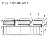
- FIG. 3 is a sectional view showing a structure of a solar cell battery formed by connecting a plurality of conventional solar cells, which is disclosed in GaAs Interconnect Design and Weld Technology : IEEE PVSC-1985 p.633.
- each solar cell of the battery comprises an n type GaAs layer 2 and a p type GaAs layer 3 formed on an n type GaAs substrate 1 and a cover glass 5 is attached thereon by a first adhesive 4.
- an upper electrode of a first solar cell is connected to a lower electrode of a second solar cell by an interconnector 6 and then an upper electrode of the second solar cell is connected to a lower electrode of a third solar cell and so forth.
- the upper electrode of one solar cell is connected to the lower electrode of the adjacent solar cell by the interconnector 6, whereby a predetermined number of solar cells are connected in series. Then, these connected plurality of solar cells are arranged and fixed onto a honeycomb board 8 by a second adhesive 7 and then the solar cell battery is completed.
- the constituent solar cells are each separate and the degree of freedom in designing layout is low.
- the p side electrode and the n side electrode are formed on the upper and lower surfaces of each solar cell respectively, it is necessary to connect the upper electrode of one solar cell to the lower electrode of the adjacent solar cell during construction.
- it is difficult to connect two electrodes by the interconnector 6 because there is a large step difference because of the thickness of each solar cell and also the structure of each interconnector 6 results in complication.
- each solar cell has a substrate having opposed front and back major surfaces, a crystalline semiconductor layer of a first conductivity type on the front major surface of said substrate, a crystalline semiconductor layer of a second conductivity type on said layer of the first conductivity type, an electrode of the first conductivity type on the back major surface of said substrate;and an electrode of the second conductivity type having interconnected first and second portions on a front surface of said layer of the second conductivity type and the back major surface of said substrate, respectively; wherein: said electrode of the first conductivity type of each solar cell is connected to a respective electrode of the second conductivity type of an adjacent one of the plurality of solar cells at the back major surface of said substrate of each solar cell.
- each cell the substrate, which is of n-type conductivity GaAs, is diffused from each surface with the dopant to form an isolation diffusion extending through the substrate.
- Each front and back portion of a p-type conductivity electrode is formed each side of this isolation diffusion, front and back.
- the solar cells are separated from a common substrate wafer; and assembled to produce a solar cell battery in which the respective of the front and back portions of the p-type conductivity electrodes are interconnected and the p-type and n-type conductivity electrodes of adjacent solar cells are connected in series at the back of the assembly.
- the present invention is intended as a solution to these problems aforesaid and it is an object of the present invention to provide a method of manufacturing a solar cell battery in which a plurality of solar cells are integrated as part of a common substrate wafer, the wiring structure and connecting work therefor are simple, and further a large physical stress is not applied at the time of connecting work and the electrical characteristics of each cell are not degraded.
- a method of manufacturing a solar cell battery and a solar cell battery, each in accordance with the present invention are defined in claims 1 and 3 of the claims appended.
- the preamble of claim 3 is based on features which also are known from JP-A-1 82571, just mentioned.
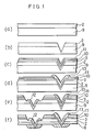
- Figure 2 is a sectional view showing how the heteroface type GaAs solar cells manufactured as above are integrated on a common substrate wafer.
- reference numeral 14 designates wiring metal connecting each respective p-type conductivity electrode 13 to a respective n-type conductivity electrode 12.
- Reference numeral 15 designates a trench formed so as to reach the semi-insulating GaAs substrate 9 to prevent electrical short-circuiting between adjacent solar cells.
- the wiring metal 14 connects each respective n-type conductivity electrode 12 on the back surface of each respective solar cell to the corresponding respective p-type conductivity electrode 13 on the back surface of the adjacent solar cell.
- each p-n junction is provided by the semi-insulating GaAs substrate 9, and the electrodes 12, 13 of the first and second conductivity types are formed in concavities in the solar cell active regions, and while connecting a plurality of solar cells, electrodes exposed on the back surface of the substrate 9 are sequentially connected to the respective electrodes of the adjacent solar cells, and finally trenches 15 are provided between the adjacent solar cells so as to reach the semi-insulating GaAs substrate 9.
- a plurality of solar cells can be formed on one wafer by a simple fabrication technique. While connecting the plurality of solar cells to constitute a solar cell battery, a step difference is not present at each connector and the wiring structure and the connecting work can be simple and easy. Furthermore, physical stress at the time of connection is reduced.
- the substrate is not limited to this and insulating material such as sapphire or InP or semi-insulating material other than GaAs can be used.
- GaAs or AlGaAs is used as a material of the active region of the solar cell in the above embodiment, a material such as InP, GaAsP or InGaAsP can be used.
Landscapes
- Photovoltaic Devices (AREA)
Claims (5)
- Verfahren zur Herstellung einer Solarzellenbatterie, wobei das Verfahren die folgenden Schritte aufweist:
das Vorsehen eines Substrats (9) aus isolierendem oder halbisolierendem Material mit vorderer und hinterer Hauptfläche, die entgegengesetzt zueinander liegen,
das Ausbilden einer kristallinen Halbleiterschicht (2) eines Typs mit erster Leitfähigkeit auf der vorderen Hauptfläche des Substrats (9),
das auswählende Ätzen der Schicht (2) des Typs mit erster Leitfähigkeit und des Substrats (9), um erste Höhlungen auszubilden, die in den Körper des Substrats (9) reichen,
das Ausbilden einer kristallinen Halbleiterschicht (3) eines Typs mit zweiter Leitfähigkeit auf der Oberfläche der Schicht (2) des Typs mit erster Leitfähigkeit und auf den jeweiligen Oberflächen der ersten Höhlungen, die durch Ätzen freigelegt sind,
das Ausbilden jeweiliger Elektroden (13) des Typs mit zweiter Leitfähigkeit auf der Oberfläche der Schicht (3) des Typs mit zweiter Leitfähigkeit über jeder ersten Höhlung,
das auswählende Ätzen der Schichten (3, 2) der Typen mit zweiter bzw. erster Leitfähigkeit und des Substrats (9), um zweite Höhlungen auszubilden, die in den Körper des Substrats (9) reichen,
das Ausbilden jeweiliger Elektroden (12) des Typs mit erster Leitfähigkeit auf den Oberflächen der Schicht (2) des Typs mit erster Leitfähigkeit und des Substrats (9) an den jeweiligen Oberflächen der zweiten Höhlungen, die durch Ätzen freigelegt sind,
das Entfernen von Substratmaterial durch Ätzen oder Schleifen der hinteren Hauptfläche des Substrats (9), um die Elektroden (12, 13) der Typen mit erster bzw. zweiter Leitfähigkeit freizulegen,
das Zufügen von Elektrodenmaterial von den Typen mit erster bzw. zweiter Leitfähigkeit zu den Elektroden (12,13) der Typen mit erster bzw. zweiter Leitfähigkeit zum Verstärken von diesen an der hinteren Fläche des Substrats (9),
das Verbinden der Elektroden (12) des Typs mit erster Leitfähigkeit mit jeweiligen benachbarten Elektroden (13) des Typs mit zweiter Leitfähigkeit über ein Verdrahtungsmetall (14) an der hinteren Fläche des Substrats (9) und
das Ausbilden von Gräben (15) zum Isolieren und Beschreiben benachbarter Solarzellenabschnitte (2, 3, 12, 13) der Solarzellenbatterie, wobei sich die Gräben (15) durch beide Schichten (3, 2) der Typen mit zweiter bzw. erster Leitfähigkeit erstrecken und das Substrat (9) erreichen. - Verfahren zur Herstellung einer Solarzellenbatterie nach Anspruch 1, das ferner die Schritte des Aufbringens eines Klebemittels (4) auf die vordere Fläche der Batterie und das Positionieren eines Abdeckglases (5) auf diesem beinhaltet.
- Solarzellenbatterie, die eine Vielzahl von Solarzellen (2, 3, 9, 12, 13) aufweist, wobei jede Solarzelle (2, 3, 9, 12, 13) aufweist: ein Substrat (9) mit vorderer und hinterer Hauptfläche, die entgegengesetzt zueinander liegen, eine kristalline Halbleiterschicht (2) eines Typs mit erster Leitfähigkeit auf der vorderen Hauptfläche des Substrats (9), eine kristalline Halbleiterschicht (3) eines Typs mit zweiter Leitfähigkeit auf der Schicht (2) des Typs mit erster Leitfähigkeit, eine Elektrode (12) des Typs mit erster Leitfähigkeit auf der hinteren Hauptfläche des Substrats (9) und
eine Elektrode (13) des Typs mit zweiter Leitfähigkeit, die erste und zweite Abschnitte, die miteinander verbunden sind, auf einer vorderen Fläche der Schicht (3) des Typs mit zweiter Leitfähigkeit bzw. der hinteren Hauptfläche des Substrats (9) aufweist, wobei
die Elektrode (12) des Typs mit erster Leitfähigkeit jeder Solarzelle (2, 3, 9, 12, 13) mit einer jeweiligen Elektrode (13) des Typs mit zweiter Leitfähigkeit einer benachbarten der Vielzahl von Solarzellen (2, 3, 9, 12, 13) an der hinteren Hauptfläche des Substrats (9) jeder Solarzelle (2, 3, 9, 12, 13) verbunden (14) ist,
wobei die Solarzellenbatterie dadurch gekennzeichnet ist, daß
das Substrat (9) jeder Solarzelle (2, 3, 9, 12, 13) ein Substrat (9) ist, daß der Vielzahl von Solarzellen (2, 3, 9, 12, 13) gemeinsam ist, und aus einem isolierenden oder halbisolierenden Material ist,
die Solarzellen (2, 3, 9, 12, 13) durch Gräben (15) zur Isolierung beschrieben sind, wobei sich die Gräben (15) durch beide Schichten (3, 2) der Typen mit zweiter bzw. erster Leitfähigkeit erstrecken und das Substrat (9) erreichen,
jede Elektrode (12) des Typs mit erster Leitfähigkeit sich durch das Substrat (9) erstreckt und die Schicht (2) des Typs mit erster Leitfähigkeit einer jeweiligen der Vielzahl von Solarzellen (2, 3, 9, 12, 13) berührt und
jede Elektrode (13) des Typs mit zweiter Leitfähigkeit sich durch das Substrat (9) erstreckt und die Schicht (3) des Typs mit zweiter Leitfähigkeit einer jeweiligen der Vielzahl von Solarzellen (2, 3, 9, 12, 13) berührt, wobei die Schicht (3) des Typs mit zweiter Leitfähigkeit zwischen der Elektrode (13) des Typs mit zweiter Leitfähigkeit und sowohl dem Substrat (9) als auch der Schicht (2) des Typs mit erster Leitfähigkeit in einer entsprechenden Höhlung in diesen liegt. - Solarzellenbatterie nach Anspruch 3, wobei auf der vorderen Fläche der Batterie ein Klebemittel (4) vorhanden ist und sich ein Abdeckglas (5) darauf befindet.
- Solarzellenbatterie nach Anspruch 3 oder 4, wobei das Substrat (9) ein halbisolierendes GaAs-Substrat ist und die Schichten (2, 3) des Typs mit erster bzw. zweiter Leitfähigkeit epitaxiale Kristallschichten aus GaAs vom n-Typ bzw. vom p-Typ sind.
Applications Claiming Priority (2)
| Application Number | Priority Date | Filing Date | Title |
|---|---|---|---|
| JP2102633A JPH0831617B2 (ja) | 1990-04-18 | 1990-04-18 | 太陽電池及びその製造方法 |
| JP102633/90 | 1990-04-18 |
Publications (2)
| Publication Number | Publication Date |
|---|---|
| EP0452588A1 EP0452588A1 (de) | 1991-10-23 |
| EP0452588B1 true EP0452588B1 (de) | 1995-12-27 |
Family
ID=14332645
Family Applications (1)
| Application Number | Title | Priority Date | Filing Date |
|---|---|---|---|
| EP90311836A Expired - Lifetime EP0452588B1 (de) | 1990-04-18 | 1990-10-29 | Solarzelle und Verfahren zu ihrer Herstellung |
Country Status (4)
| Country | Link |
|---|---|
| US (1) | US5100480A (de) |
| EP (1) | EP0452588B1 (de) |
| JP (1) | JPH0831617B2 (de) |
| DE (1) | DE69024481T2 (de) |
Cited By (5)
| Publication number | Priority date | Publication date | Assignee | Title |
|---|---|---|---|---|
| US7831151B2 (en) | 2001-06-29 | 2010-11-09 | John Trezza | Redundant optical device array |
| US7838868B2 (en) | 2005-01-20 | 2010-11-23 | Nanosolar, Inc. | Optoelectronic architecture having compound conducting substrate |
| CN101656273B (zh) * | 2008-08-18 | 2011-07-13 | 中芯国际集成电路制造(上海)有限公司 | 选择性发射极太阳能电池单元及其制造方法 |
| US8198117B2 (en) | 2005-08-16 | 2012-06-12 | Nanosolar, Inc. | Photovoltaic devices with conductive barrier layers and foil substrates |
| US8247243B2 (en) | 2009-05-22 | 2012-08-21 | Nanosolar, Inc. | Solar cell interconnection |
Families Citing this family (49)
| Publication number | Priority date | Publication date | Assignee | Title |
|---|---|---|---|---|
| JPH10508987A (ja) * | 1995-05-19 | 1998-09-02 | ドクトル・ヨハネス・ハイデンハイン・ゲゼルシャフト・ミト・ベシュレンクテル・ハフツング | 光検出器素子及びその製造方法 |
| DE19549228A1 (de) * | 1995-12-21 | 1997-06-26 | Heidenhain Gmbh Dr Johannes | Optoelektronisches Sensor-Bauelement |
| DE19758589B4 (de) * | 1996-04-26 | 2004-05-13 | Mitsubishi Denki K.K. | Solarzelle und Verfahren zur Herstellung von Solarzellen |
| DE19706519B4 (de) * | 1996-04-26 | 2004-02-05 | Mitsubishi Denki K.K. | Verfahren zur Herstellung von Solarzellen |
| US6034321A (en) * | 1998-03-24 | 2000-03-07 | Essential Research, Inc. | Dot-junction photovoltaic cells using high-absorption semiconductors |
| US6753199B2 (en) * | 2001-06-29 | 2004-06-22 | Xanoptix, Inc. | Topside active optical device apparatus and method |
| KR100918512B1 (ko) * | 2001-06-29 | 2009-09-24 | 큐빅 웨이퍼 인코포레이티드 | 광전자 소자 집적 |
| US6775308B2 (en) | 2001-06-29 | 2004-08-10 | Xanoptix, Inc. | Multi-wavelength semiconductor laser arrays and applications thereof |
| US6724794B2 (en) * | 2001-06-29 | 2004-04-20 | Xanoptix, Inc. | Opto-electronic device integration |
| US6753197B2 (en) | 2001-06-29 | 2004-06-22 | Xanoptix, Inc. | Opto-electronic device integration |
| US6790691B2 (en) * | 2001-06-29 | 2004-09-14 | Xanoptix, Inc. | Opto-electronic device integration |
| US6633421B2 (en) | 2001-06-29 | 2003-10-14 | Xanoptrix, Inc. | Integrated arrays of modulators and lasers on electronics |
| US6731665B2 (en) | 2001-06-29 | 2004-05-04 | Xanoptix Inc. | Laser arrays for high power fiber amplifier pumps |
| US6620642B2 (en) | 2001-06-29 | 2003-09-16 | Xanoptix, Inc. | Opto-electronic device integration |
| JP4110390B2 (ja) * | 2002-03-19 | 2008-07-02 | セイコーエプソン株式会社 | 半導体装置の製造方法 |
| WO2004068665A2 (en) * | 2003-01-24 | 2004-08-12 | The Board Of Trustees Of The University Of Arkansas Research And Sponsored Programs | Wafer scale packaging technique for sealed optical elements and sealed packages produced thereby |
| US7649141B2 (en) | 2003-06-30 | 2010-01-19 | Advent Solar, Inc. | Emitter wrap-through back contact solar cells on thin silicon wafers |
| US7144751B2 (en) | 2004-02-05 | 2006-12-05 | Advent Solar, Inc. | Back-contact solar cells and methods for fabrication |
| US7335555B2 (en) | 2004-02-05 | 2008-02-26 | Advent Solar, Inc. | Buried-contact solar cells with self-doping contacts |
| US20050172996A1 (en) | 2004-02-05 | 2005-08-11 | Advent Solar, Inc. | Contact fabrication of emitter wrap-through back contact silicon solar cells |
| US7276724B2 (en) | 2005-01-20 | 2007-10-02 | Nanosolar, Inc. | Series interconnected optoelectronic device module assembly |
| JP4681352B2 (ja) * | 2005-05-24 | 2011-05-11 | 本田技研工業株式会社 | カルコパイライト型太陽電池 |
| US7534722B2 (en) | 2005-06-14 | 2009-05-19 | John Trezza | Back-to-front via process |
| US7560813B2 (en) | 2005-06-14 | 2009-07-14 | John Trezza | Chip-based thermo-stack |
| US20060281303A1 (en) * | 2005-06-14 | 2006-12-14 | John Trezza | Tack & fuse chip bonding |
| US7687400B2 (en) * | 2005-06-14 | 2010-03-30 | John Trezza | Side stacking apparatus and method |
| US7838997B2 (en) * | 2005-06-14 | 2010-11-23 | John Trezza | Remote chip attachment |
| US20060278996A1 (en) * | 2005-06-14 | 2006-12-14 | John Trezza | Active packaging |
| US7786592B2 (en) | 2005-06-14 | 2010-08-31 | John Trezza | Chip capacitive coupling |
| US8456015B2 (en) * | 2005-06-14 | 2013-06-04 | Cufer Asset Ltd. L.L.C. | Triaxial through-chip connection |
| US7946331B2 (en) * | 2005-06-14 | 2011-05-24 | Cufer Asset Ltd. L.L.C. | Pin-type chip tooling |
| US7521806B2 (en) * | 2005-06-14 | 2009-04-21 | John Trezza | Chip spanning connection |
| US7781886B2 (en) * | 2005-06-14 | 2010-08-24 | John Trezza | Electronic chip contact structure |
| US7851348B2 (en) * | 2005-06-14 | 2010-12-14 | Abhay Misra | Routingless chip architecture |
| US7767493B2 (en) * | 2005-06-14 | 2010-08-03 | John Trezza | Post & penetration interconnection |
| US20070281460A1 (en) * | 2006-06-06 | 2007-12-06 | Cubic Wafer, Inc. | Front-end processed wafer having through-chip connections |
| US7687397B2 (en) * | 2006-06-06 | 2010-03-30 | John Trezza | Front-end processed wafer having through-chip connections |
| KR101175393B1 (ko) * | 2006-10-17 | 2012-08-20 | 쿠퍼 에셋 엘티디. 엘.엘.씨. | 웨이퍼 비아 형성 |
| US7705613B2 (en) * | 2007-01-03 | 2010-04-27 | Abhay Misra | Sensitivity capacitive sensor |
| US7670874B2 (en) | 2007-02-16 | 2010-03-02 | John Trezza | Plated pillar package formation |
| US7748116B2 (en) * | 2007-04-05 | 2010-07-06 | John Trezza | Mobile binding in an electronic connection |
| US7850060B2 (en) * | 2007-04-05 | 2010-12-14 | John Trezza | Heat cycle-able connection |
| US7960210B2 (en) * | 2007-04-23 | 2011-06-14 | Cufer Asset Ltd. L.L.C. | Ultra-thin chip packaging |
| KR101028971B1 (ko) * | 2009-05-26 | 2011-04-19 | 한국과학기술원 | 집적형 박막 태양전지 및 그의 제조 방법 |
| KR101091475B1 (ko) * | 2009-06-30 | 2011-12-07 | 엘지이노텍 주식회사 | 태양전지 및 이의 제조방법 |
| KR101676368B1 (ko) * | 2010-03-05 | 2016-11-15 | 주성엔지니어링(주) | 태양전지 및 그 제조방법 |
| FR2961300B1 (fr) * | 2010-06-14 | 2014-05-09 | Inst Rech Fondamentale En Technologies Solaires Irfts | Structure de solidarisation de panneaux photovoltaiques sur un bati |
| KR20150039535A (ko) * | 2013-10-02 | 2015-04-10 | 엘지이노텍 주식회사 | 태양전지 및 이의 제조방법 |
| CN106611803B (zh) * | 2015-10-19 | 2019-04-23 | 北京创昱科技有限公司 | 一种太阳能电池片、其制备方法及其组成的太阳能电池组 |
Family Cites Families (12)
| Publication number | Priority date | Publication date | Assignee | Title |
|---|---|---|---|---|
| GB1010476A (en) * | 1962-01-15 | 1965-11-17 | Secr Aviation | Improved photo-electric generators |
| US4110122A (en) * | 1976-05-26 | 1978-08-29 | Massachusetts Institute Of Technology | High-intensity, solid-state-solar cell device |
| US4156309A (en) * | 1977-12-23 | 1979-05-29 | The United States Of America As Represented By The Administrator Of The National Aeronautics And Space Administration | Method of construction of a multi-cell solar array |
| FR2426335A1 (fr) * | 1978-05-19 | 1979-12-14 | Radiotechnique Compelec | Dispositif semi-conducteur monolithique comportant une pluralite de cellules photosensibles |
| US4200472A (en) * | 1978-06-05 | 1980-04-29 | The Regents Of The University Of California | Solar power system and high efficiency photovoltaic cells used therein |
| US4278473A (en) * | 1979-08-24 | 1981-07-14 | Varian Associates, Inc. | Monolithic series-connected solar cell |
| US4335503A (en) * | 1980-12-24 | 1982-06-22 | The United States Of America As Represented By The Administrator Of The National Aeronautics And Space Administration | Method of making a high voltage V-groove solar cell |
| JPS58201376A (ja) * | 1982-05-20 | 1983-11-24 | Toshiba Corp | 太陽電池装置 |
| JPS63211773A (ja) * | 1987-02-27 | 1988-09-02 | Mitsubishi Electric Corp | 化合物半導体太陽電池 |
| JPS6482571A (en) * | 1987-09-24 | 1989-03-28 | Mitsubishi Electric Corp | Solar cell and manufacture thereof |
| JPS6482570A (en) * | 1987-09-24 | 1989-03-28 | Mitsubishi Electric Corp | Manufacture of photoelectric conversion device |
| US4897123A (en) * | 1987-11-28 | 1990-01-30 | Mitsubishi Denki Kabushiki Kaisha | Solar cells and method for producing solar cells |
-
1990
- 1990-04-18 JP JP2102633A patent/JPH0831617B2/ja not_active Expired - Lifetime
- 1990-10-29 DE DE69024481T patent/DE69024481T2/de not_active Expired - Fee Related
- 1990-10-29 EP EP90311836A patent/EP0452588B1/de not_active Expired - Lifetime
- 1990-10-31 US US07/606,853 patent/US5100480A/en not_active Expired - Fee Related
Cited By (8)
| Publication number | Priority date | Publication date | Assignee | Title |
|---|---|---|---|---|
| US7831151B2 (en) | 2001-06-29 | 2010-11-09 | John Trezza | Redundant optical device array |
| US8525152B2 (en) | 2004-09-18 | 2013-09-03 | Nanosolar, Inc. | Formation of solar cells with conductive barrier layers and foil substrates |
| US7838868B2 (en) | 2005-01-20 | 2010-11-23 | Nanosolar, Inc. | Optoelectronic architecture having compound conducting substrate |
| US7919337B2 (en) | 2005-01-20 | 2011-04-05 | Nanosolar, Inc. | Optoelectronic architecture having compound conducting substrate |
| US7968869B2 (en) | 2005-01-20 | 2011-06-28 | Nanosolar, Inc. | Optoelectronic architecture having compound conducting substrate |
| US8198117B2 (en) | 2005-08-16 | 2012-06-12 | Nanosolar, Inc. | Photovoltaic devices with conductive barrier layers and foil substrates |
| CN101656273B (zh) * | 2008-08-18 | 2011-07-13 | 中芯国际集成电路制造(上海)有限公司 | 选择性发射极太阳能电池单元及其制造方法 |
| US8247243B2 (en) | 2009-05-22 | 2012-08-21 | Nanosolar, Inc. | Solar cell interconnection |
Also Published As
| Publication number | Publication date |
|---|---|
| DE69024481T2 (de) | 1996-05-09 |
| JPH0831617B2 (ja) | 1996-03-27 |
| JPH042174A (ja) | 1992-01-07 |
| DE69024481D1 (de) | 1996-02-08 |
| US5100480A (en) | 1992-03-31 |
| EP0452588A1 (de) | 1991-10-23 |
Similar Documents
| Publication | Publication Date | Title |
|---|---|---|
| EP0452588B1 (de) | Solarzelle und Verfahren zu ihrer Herstellung | |
| EP1125331B1 (de) | Monolitische bypass-diode und solarzellenband-zusammenbau | |
| EP0768720B1 (de) | Solarzelle mit integrierter Umleitungsdiode und Herstellungsverfahren | |
| US7449630B2 (en) | Solar cell having an integral monolithically grown bypass diode | |
| US5391236A (en) | Photovoltaic microarray structure and fabrication method | |
| US5716459A (en) | Monolithically integrated solar cell microarray and fabrication method | |
| CN101237007B (zh) | 具有用于背侧接点的通孔的倒置变形太阳能电池 | |
| EP0666602B1 (de) | Herstellungsverfahren einer GaAs Solarzelle auf einem Si-Substrat | |
| JPH05110121A (ja) | 太陽電池 | |
| EP1008188B1 (de) | Solarzelle mit einer integrierten monolitisch gewachsenen Bypassdiode | |
| US4846896A (en) | Solar cell with integral reverse voltage protection diode | |
| JP4009106B2 (ja) | 半導体受光素子、及びその製造方法 | |
| JPH0747878Y2 (ja) | 太陽電池セル | |
| WO1999062125A1 (en) | Solar cell having an integral monolithically grown bypass diode | |
| US5131956A (en) | Photovoltaic semiconductor device | |
| US4935067A (en) | Solar cell and fabrication method thereof | |
| EP1428267B1 (de) | Solarzelle mit bypassdiode zum schutz gegen inverse vorspannung | |
| JPH0548134A (ja) | 太陽電池とその製造方法 | |
| EP2197042A2 (de) | Solarzellen mit einer integralen monolithisch gewachsenen Bypass-Diode | |
| JPH043471A (ja) | 太陽電池 | |
| JPH0451575A (ja) | 太陽電池およびその製造方法 |
Legal Events
| Date | Code | Title | Description |
|---|---|---|---|
| PUAI | Public reference made under article 153(3) epc to a published international application that has entered the european phase |
Free format text: ORIGINAL CODE: 0009012 |
|
| 17P | Request for examination filed |
Effective date: 19901228 |
|
| AK | Designated contracting states |
Kind code of ref document: A1 Designated state(s): DE FR GB |
|
| 17Q | First examination report despatched |
Effective date: 19940310 |
|
| GRAA | (expected) grant |
Free format text: ORIGINAL CODE: 0009210 |
|
| AK | Designated contracting states |
Kind code of ref document: B1 Designated state(s): DE FR GB |
|
| REF | Corresponds to: |
Ref document number: 69024481 Country of ref document: DE Date of ref document: 19960208 |
|
| ET | Fr: translation filed | ||
| PLBE | No opposition filed within time limit |
Free format text: ORIGINAL CODE: 0009261 |
|
| STAA | Information on the status of an ep patent application or granted ep patent |
Free format text: STATUS: NO OPPOSITION FILED WITHIN TIME LIMIT |
|
| 26N | No opposition filed | ||
| PGFP | Annual fee paid to national office [announced via postgrant information from national office to epo] |
Ref country code: FR Payment date: 19981009 Year of fee payment: 9 |
|
| PGFP | Annual fee paid to national office [announced via postgrant information from national office to epo] |
Ref country code: GB Payment date: 19981030 Year of fee payment: 9 |
|
| PGFP | Annual fee paid to national office [announced via postgrant information from national office to epo] |
Ref country code: DE Payment date: 19981106 Year of fee payment: 9 |
|
| PG25 | Lapsed in a contracting state [announced via postgrant information from national office to epo] |
Ref country code: GB Free format text: LAPSE BECAUSE OF NON-PAYMENT OF DUE FEES Effective date: 19991029 |
|
| GBPC | Gb: european patent ceased through non-payment of renewal fee |
Effective date: 19991029 |
|
| PG25 | Lapsed in a contracting state [announced via postgrant information from national office to epo] |
Ref country code: FR Free format text: LAPSE BECAUSE OF NON-PAYMENT OF DUE FEES Effective date: 20000630 |
|
| PG25 | Lapsed in a contracting state [announced via postgrant information from national office to epo] |
Ref country code: DE Free format text: LAPSE BECAUSE OF NON-PAYMENT OF DUE FEES Effective date: 20000801 |
|
| REG | Reference to a national code |
Ref country code: FR Ref legal event code: ST |