EP0452661B1 - Structures d'une jonction métal-isolant-métal ayant une hauteur de barrières ajustables et sa méthode de fabrication - Google Patents
Structures d'une jonction métal-isolant-métal ayant une hauteur de barrières ajustables et sa méthode de fabrication Download PDFInfo
- Publication number
- EP0452661B1 EP0452661B1 EP91103562A EP91103562A EP0452661B1 EP 0452661 B1 EP0452661 B1 EP 0452661B1 EP 91103562 A EP91103562 A EP 91103562A EP 91103562 A EP91103562 A EP 91103562A EP 0452661 B1 EP0452661 B1 EP 0452661B1
- Authority
- EP
- European Patent Office
- Prior art keywords
- metal
- barrier
- semiconductor
- polycrystalline
- barrier material
- Prior art date
- Legal status (The legal status is an assumption and is not a legal conclusion. Google has not performed a legal analysis and makes no representation as to the accuracy of the status listed.)
- Expired - Lifetime
Links
Images


Classifications
-
- H—ELECTRICITY
- H10—SEMICONDUCTOR DEVICES; ELECTRIC SOLID-STATE DEVICES NOT OTHERWISE PROVIDED FOR
- H10N—ELECTRIC SOLID-STATE DEVICES NOT OTHERWISE PROVIDED FOR
- H10N70/00—Solid-state devices having no potential barriers, and specially adapted for rectifying, amplifying, oscillating or switching
-
- Y—GENERAL TAGGING OF NEW TECHNOLOGICAL DEVELOPMENTS; GENERAL TAGGING OF CROSS-SECTIONAL TECHNOLOGIES SPANNING OVER SEVERAL SECTIONS OF THE IPC; TECHNICAL SUBJECTS COVERED BY FORMER USPC CROSS-REFERENCE ART COLLECTIONS [XRACs] AND DIGESTS
- Y10—TECHNICAL SUBJECTS COVERED BY FORMER USPC
- Y10S—TECHNICAL SUBJECTS COVERED BY FORMER USPC CROSS-REFERENCE ART COLLECTIONS [XRACs] AND DIGESTS
- Y10S148/00—Metal treatment
- Y10S148/139—Schottky barrier
-
- Y—GENERAL TAGGING OF NEW TECHNOLOGICAL DEVELOPMENTS; GENERAL TAGGING OF CROSS-SECTIONAL TECHNOLOGIES SPANNING OVER SEVERAL SECTIONS OF THE IPC; TECHNICAL SUBJECTS COVERED BY FORMER USPC CROSS-REFERENCE ART COLLECTIONS [XRACs] AND DIGESTS
- Y10—TECHNICAL SUBJECTS COVERED BY FORMER USPC
- Y10S—TECHNICAL SUBJECTS COVERED BY FORMER USPC CROSS-REFERENCE ART COLLECTIONS [XRACs] AND DIGESTS
- Y10S148/00—Metal treatment
- Y10S148/14—Schottky barrier contacts
-
- Y—GENERAL TAGGING OF NEW TECHNOLOGICAL DEVELOPMENTS; GENERAL TAGGING OF CROSS-SECTIONAL TECHNOLOGIES SPANNING OVER SEVERAL SECTIONS OF THE IPC; TECHNICAL SUBJECTS COVERED BY FORMER USPC CROSS-REFERENCE ART COLLECTIONS [XRACs] AND DIGESTS
- Y10—TECHNICAL SUBJECTS COVERED BY FORMER USPC
- Y10S—TECHNICAL SUBJECTS COVERED BY FORMER USPC CROSS-REFERENCE ART COLLECTIONS [XRACs] AND DIGESTS
- Y10S148/00—Metal treatment
- Y10S148/142—Semiconductor-metal-semiconductor
Definitions
- U.S. Patent 3,056,073 issued September 25, 1986 to Mead entitled SOLID-STATE ELECTRON DEVICES describes a tunnel diode structure wherein two metal plates with an applied electric field are separated by an insulating layer and electrons as one metal plate tunneling barrier therebetween comprised of silicon, germanium or an alloy thereof preferably deposited on the lower superconductive electrodes by chemical vapor deposition.
- the barrier height of the junction is precisely controlled by precision doping of the semiconductor material.
- U.S. Patent 3,448,350 issued June 3, 1969 to Yamashita et al entitled SEMICONDUCTOR COMPRISING PLURAL DEEP-LEVEL-FORMING IMPURITIES describes a semiconductor device comprising a body of semiconductor material such as a III-V compound, Si or Ge doped with at least two deep-level-forming impurities. At least two electrodes are provided to the semiconductor body. The body may have additional regions of p, n, p+ and n+ conductivity formed therein.
- U.S. Patent 4,220,959 issued September 2, 1980 to Kroger entitled JOSEPHSON TUNNEL JUNCTION WITH POLYCRYSTALLINE SILICON, GERMANIUM OR SILICON-GERMANIUM ALLOY TUNNELING BARRIER, describes a structure wherein a Josephson tunnel junction device having niobium nitride superconductive electrodes includes a polycrystalline semiconductor tunneling barrier therebetween comprised of silicon, germanium or an alloy thereof preferably deposited on the lower superconductive electrodes by chemical vapor depostion. The barrier height of the junction is precisely controlled by precision doping of the semiconductor material.
- IBM Technical Disclosure Bulletin, Vol. 31, No. 2, July 1988 at page 383 describes a technique whereby ohmic contacts are prepared so as to produce thermally-stable low-resistance contacts. Two preparation methods are described: Indium-Germanium coevaporation and implantation of indium through the contact metals.
- the present invention uses a multi-alloy semiconductor as the barrier material.
- the material is selected from a materials system in which the barrier height is a function of alloy composition.
- Fermi level pinning means that the Fermi level is forced to have a certain value at a surface or interface due to a high density of surface or interface states.
- the fact that the Fermi level is pinned at a surface at an energy different from its value in the bulk of the material implies band bending and surface charges.
- a method for fabricating junctions having metal electrodes separated by polycrystalline barriers with arbitrarily-chosen but controlled barrier height and shape is accomplished by varying the composition and doping of polycrystalline multinary compound semiconductor materials in the barrier, hence varying the Fermi level pinning position such that the Fermi level is fixed and controlled at and everywhere in between the two metal-insulator interfaces. This situation exists virtually independent of the doping.
- the basic structure is illustrated schematically in FIG. 1.
- the metal electrodes need not be single crystalline, and their crystal structures need have no particular relationship to that of the barrier. They can be normal metals or superconductors.
- the barrier consists of a compound semiconductor, and is polycrystalline in nature.
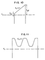
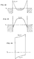
- FIG. 12 This structure could be achieved, for example, in the case d >> t using pure polycrystalline GaAs and doping at 5x1017 cm ⁇ 3. Alternatively, in the case d >> L D , with lightly-doped material, one can vary x from ⁇ 0 to ⁇ 1 and back.
Landscapes
- Electrodes Of Semiconductors (AREA)
Claims (6)
- Procédé pour fabriquer des jonctions composées de deux électrodes séparées par une barrière polycristalline comprenant les étapes consistant à :
déposer un matériau semiconducteur polycristallin de barrière sur une première électrode formant une première interface et une barrière à semiconducteur
déposer un seconde électrode constituée de métal sur ladite barrière à semiconducteur à une seconde interface, caractérisée
en ce que la première électrode est constituée de métal,
en ce que pour le dépôt du matériau semiconducteur polycristallin de barrière un alliage multinaire semiconducteur du dosage choisi est utilisé, dans lequel ledit alliage multinaire semiconducteur a une composition étant dosée dans le contenu des alliages séparés, et
en ce que le dosage de la composition d'alliage multinaire semiconducteur est déterminé afin d'obtenir des barrières de formes choisies en procurant des positions de blocage du niveau de Fermi à des valeurs choisies auxdites interfaces métal-semiconducteur et aux limites de granules dudit matériau semiconducteur polycristallin de barrière. - Procédé selon la revendication 1, comportant de plus l'étape consistant à doper ledit alliage multinaire semiconducteur dosé avec des dopants déterminés, dans lequel ledit dépôt dudit alliage multinaire semiconducteur dosé déterminé en combinaison avec le dopage engendre, la forme de barrière déterminée désirée.
- Procédé selon la revendication 1 ou 2, caractérisé en ce que le diamètre des granules du matériau semiconducteur polycristallin de barrière est ajusté eu égard à la forme de barrière désirée entre lesdites première et seconde électrodes métalliques.
- Procédé selon la revendication 3, caractérisé en ce que le diamètre des granules du matériau semiconducteur polycristallin de barrière est inférieur à la distance entre lesdites première et seconde électrodes.
- Procédé selon la revendication 3 ou 4, dans lequel la position de blocage du niveau de Fermi auxdits premier et second interfaces desdites limites de granules dudit matériau semiconducteur polycristallin de barrière est uniforme afin de procurer une barrière homogène.
- Structure à couche comprenant deux électrodes prenant en sandwich un matériau semiconducteur polycristallin de barrière entre elles, caractérisée
en ce que les deux électrodes sont constituées d'un métal, et
en ce que le matériau semiconducteur polycristallin de barrière est constitué d'un alliage multinaire semiconducteur ayant une composition qui est dosée dans le contenu des alliages multinaires séparés, dans lequel le dosage de la composition d'alliage multinaire semiconducteur est déterminé pour procurer des positions de blocage du niveaux de Fermi choisies aux interfaces métal-semiconducteur et aux limites de granules du matériau semiconducteur polycristallin de barrière afin d'obtenir des barrières de formes déterminées.
Applications Claiming Priority (2)
| Application Number | Priority Date | Filing Date | Title |
|---|---|---|---|
| US07/512,245 US5019530A (en) | 1990-04-20 | 1990-04-20 | Method of making metal-insulator-metal junction structures with adjustable barrier heights |
| US512245 | 1990-04-20 |
Publications (3)
| Publication Number | Publication Date |
|---|---|
| EP0452661A2 EP0452661A2 (fr) | 1991-10-23 |
| EP0452661A3 EP0452661A3 (en) | 1991-11-27 |
| EP0452661B1 true EP0452661B1 (fr) | 1995-05-31 |
Family
ID=24038286
Family Applications (1)
| Application Number | Title | Priority Date | Filing Date |
|---|---|---|---|
| EP91103562A Expired - Lifetime EP0452661B1 (fr) | 1990-04-20 | 1991-03-08 | Structures d'une jonction métal-isolant-métal ayant une hauteur de barrières ajustables et sa méthode de fabrication |
Country Status (4)
| Country | Link |
|---|---|
| US (1) | US5019530A (fr) |
| EP (1) | EP0452661B1 (fr) |
| JP (1) | JPH0652812B2 (fr) |
| DE (1) | DE69110080T2 (fr) |
Families Citing this family (38)
| Publication number | Priority date | Publication date | Assignee | Title |
|---|---|---|---|---|
| JPH0660635A (ja) * | 1992-08-06 | 1994-03-04 | Olympus Optical Co Ltd | 強誘電体メモリ装置 |
| JP3051627B2 (ja) * | 1993-02-03 | 2000-06-12 | シャープ株式会社 | 表示装置およびその製造方法 |
| GB9317256D0 (en) * | 1993-08-19 | 1993-10-06 | Boc Group Plc | Molecular processes and apparatus therefore |
| JP2995284B2 (ja) * | 1995-08-25 | 1999-12-27 | 工業技術院長 | 電極作成方法 |
| US6396191B1 (en) | 1999-03-11 | 2002-05-28 | Eneco, Inc. | Thermal diode for energy conversion |
| JP4422917B2 (ja) | 1999-03-11 | 2010-03-03 | エネコ インコーポレイテッド | ハイブリッド熱電子エネルギー変換器およびその方法 |
| US7109408B2 (en) | 1999-03-11 | 2006-09-19 | Eneco, Inc. | Solid state energy converter |
| US6198113B1 (en) | 1999-04-22 | 2001-03-06 | Acorn Technologies, Inc. | Electrostatically operated tunneling transistor |
| DE10085066T1 (de) * | 1999-10-05 | 2002-11-21 | Seagate Technology Llc | Integrierte On-Board-Vorrichtung und Verfahren für den Schutz von magnetoresistiven Köpfen vor elektrostatischer Entladung |
| US7615402B1 (en) | 2000-07-07 | 2009-11-10 | Acorn Technologies, Inc. | Electrostatically operated tunneling transistor |
| US6507046B2 (en) * | 2001-05-11 | 2003-01-14 | Cree, Inc. | High-resistivity silicon carbide substrate for semiconductor devices with high break down voltage |
| US6563185B2 (en) | 2001-05-21 | 2003-05-13 | The Regents Of The University Of Colorado | High speed electron tunneling device and applications |
| US6779347B2 (en) | 2001-05-21 | 2004-08-24 | C.P. Baker Securities, Inc. | Solid-state thermionic refrigeration |
| US7388276B2 (en) * | 2001-05-21 | 2008-06-17 | The Regents Of The University Of Colorado | Metal-insulator varactor devices |
| US6967347B2 (en) * | 2001-05-21 | 2005-11-22 | The Regents Of The University Of Colorado | Terahertz interconnect system and applications |
| US7126151B2 (en) * | 2001-05-21 | 2006-10-24 | The Regents Of The University Of Colorado, A Body Corporate | Interconnected high speed electron tunneling devices |
| US7173275B2 (en) * | 2001-05-21 | 2007-02-06 | Regents Of The University Of Colorado | Thin-film transistors based on tunneling structures and applications |
| WO2003038499A1 (fr) * | 2001-11-01 | 2003-05-08 | Mitsubishi Rayon Co.,Ltd. | Multiplexeur/demultiplexeur optique, procede de multiplexage/demultiplexage optique et filtre optique |
| US7084423B2 (en) | 2002-08-12 | 2006-08-01 | Acorn Technologies, Inc. | Method for depinning the Fermi level of a semiconductor at an electrical junction and devices incorporating such junctions |
| US6833556B2 (en) | 2002-08-12 | 2004-12-21 | Acorn Technologies, Inc. | Insulated gate field effect transistor having passivated schottky barriers to the channel |
| US6946596B2 (en) | 2002-09-13 | 2005-09-20 | Kucherov Yan R | Tunneling-effect energy converters |
| WO2006014574A2 (fr) * | 2004-07-08 | 2006-02-09 | The Regents Of The University Of Colorado | Dispositifs varactor metal-isolant |
| KR100639990B1 (ko) * | 2004-12-08 | 2006-10-31 | 한국전자통신연구원 | 급격한 금속-절연체 전이 소자 및 그 제조방법 |
| US7615385B2 (en) | 2006-09-20 | 2009-11-10 | Hypres, Inc | Double-masking technique for increasing fabrication yield in superconducting electronics |
| US7977668B2 (en) * | 2007-05-23 | 2011-07-12 | Northwestern University | Multilayer structure with zirconium-oxide tunnel barriers and applications of same |
| CN101755338B (zh) * | 2007-07-18 | 2012-10-10 | 松下电器产业株式会社 | 电流限制元件和使用它的存储器装置 |
| US8148748B2 (en) * | 2007-09-26 | 2012-04-03 | Stmicroelectronics N.V. | Adjustable field effect rectifier |
| EP2232559B1 (fr) | 2007-09-26 | 2019-05-15 | STMicroelectronics N.V. | Redresseur à effet de champ ajustable |
| EP2384518B1 (fr) * | 2009-01-06 | 2019-09-04 | STMicroelectronics N.V. | Structures de diode à effet de champ à auto-amorçage et procédés correspondants |
| WO2010127370A2 (fr) * | 2009-05-01 | 2010-11-04 | Lakota Technologies, Inc. | Dispositif de limitation de courant série |
| JP5598015B2 (ja) * | 2010-02-23 | 2014-10-01 | 株式会社デンソー | ショットキーバリアダイオードを備えた炭化珪素半導体装置およびその製造方法 |
| WO2012037474A1 (fr) | 2010-09-17 | 2012-03-22 | The Governors Of The University Of Alberta | Dispositifs électroniques moléculaires à deux et trois bornes dotés d'un transport d'électrons balistique |
| CN107578994B (zh) | 2011-11-23 | 2020-10-30 | 阿科恩科技公司 | 通过插入界面原子单层改进与iv族半导体的金属接触 |
| WO2013158986A2 (fr) * | 2012-04-19 | 2013-10-24 | Carnegie Mellon University | Diode métal/semi-conducteur/métal à hétérojonction |
| US9543423B2 (en) | 2012-09-04 | 2017-01-10 | Carnegie Mellon University | Hot-electron transistor having multiple MSM sequences |
| US9019744B2 (en) * | 2012-12-27 | 2015-04-28 | Intermolecular, Inc. | Barrier design for steering elements |
| US9620611B1 (en) | 2016-06-17 | 2017-04-11 | Acorn Technology, Inc. | MIS contact structure with metal oxide conductor |
| DE112017005855T5 (de) | 2016-11-18 | 2019-08-01 | Acorn Technologies, Inc. | Nanodrahttransistor mit Source und Drain induziert durch elektrische Kontakte mit negativer Schottky-Barrierenhöhe |
Citations (2)
| Publication number | Priority date | Publication date | Assignee | Title |
|---|---|---|---|---|
| EP0005364A1 (fr) * | 1978-05-08 | 1979-11-14 | Sperry Corporation | Dispositifs à jonction Josephson |
| FR2813310A1 (fr) * | 2000-08-25 | 2002-03-01 | Inst Francais Du Petrole | Procede de separation de paraffines multibranchees utilisant un absorbant zeolitique de structure mixte |
Family Cites Families (15)
| Publication number | Priority date | Publication date | Assignee | Title |
|---|---|---|---|---|
| US3056073A (en) * | 1960-02-15 | 1962-09-25 | California Inst Res Found | Solid-state electron devices |
| GB1145075A (en) * | 1965-04-07 | 1969-03-12 | Matsushita Electric Industrial Co Ltd | Semiconductor device |
| FR2086887A5 (fr) * | 1970-04-13 | 1971-12-31 | Air Liquide | |
| US3938243A (en) * | 1973-02-20 | 1976-02-17 | Signetics Corporation | Schottky barrier diode semiconductor structure and method |
| US4107724A (en) * | 1974-12-17 | 1978-08-15 | U.S. Philips Corporation | Surface controlled field effect solid state device |
| US4163677A (en) * | 1978-04-28 | 1979-08-07 | Rca Corporation | Schottky barrier amorphous silicon solar cell with thin doped region adjacent metal Schottky barrier |
| US4220959A (en) * | 1979-03-23 | 1980-09-02 | Sperry Corporation | Josephson tunnel junction with polycrystalline silicon, germanium or silicon-germanium alloy tunneling barrier |
| JPS56144577A (en) * | 1980-04-10 | 1981-11-10 | Fujitsu Ltd | Production of semiconductor device |
| US4421577A (en) * | 1980-11-10 | 1983-12-20 | The Board Of Trustees Of The Leland Stanford, Junior University | Method for making Schottky barrier diodes with engineered heights |
| US4371884A (en) * | 1981-01-23 | 1983-02-01 | The United States Of America As Represented By The Secretary Of The Army | InAs-GaSb Tunnel diode |
| US4449140A (en) * | 1981-12-24 | 1984-05-15 | National Research Development Corporation | Semi-conductor barrier switching devices |
| US4638342A (en) * | 1982-09-17 | 1987-01-20 | International Business Machines Corporation | Space charge modulation device |
| US4490733A (en) * | 1982-10-15 | 1984-12-25 | Sperry Corporation | Josephson device with tunneling barrier having low density of localized states and enhanced figures of merit |
| US4946803A (en) * | 1982-12-08 | 1990-08-07 | North American Philips Corp., Signetics Division | Method for manufacturing a Schottky-type rectifier having controllable barrier height |
| JPH0624251B2 (ja) * | 1986-01-08 | 1994-03-30 | 富士通株式会社 | 光半導体装置 |
-
1990
- 1990-04-20 US US07/512,245 patent/US5019530A/en not_active Expired - Fee Related
-
1991
- 1991-02-27 JP JP3056167A patent/JPH0652812B2/ja not_active Expired - Lifetime
- 1991-03-08 EP EP91103562A patent/EP0452661B1/fr not_active Expired - Lifetime
- 1991-03-08 DE DE69110080T patent/DE69110080T2/de not_active Expired - Lifetime
Patent Citations (2)
| Publication number | Priority date | Publication date | Assignee | Title |
|---|---|---|---|---|
| EP0005364A1 (fr) * | 1978-05-08 | 1979-11-14 | Sperry Corporation | Dispositifs à jonction Josephson |
| FR2813310A1 (fr) * | 2000-08-25 | 2002-03-01 | Inst Francais Du Petrole | Procede de separation de paraffines multibranchees utilisant un absorbant zeolitique de structure mixte |
Also Published As
| Publication number | Publication date |
|---|---|
| JPH0652812B2 (ja) | 1994-07-06 |
| JPH0541551A (ja) | 1993-02-19 |
| EP0452661A2 (fr) | 1991-10-23 |
| DE69110080D1 (de) | 1995-07-06 |
| EP0452661A3 (en) | 1991-11-27 |
| DE69110080T2 (de) | 1995-12-21 |
| US5019530A (en) | 1991-05-28 |
Similar Documents
| Publication | Publication Date | Title |
|---|---|---|
| US5019530A (en) | Method of making metal-insulator-metal junction structures with adjustable barrier heights | |
| US4173763A (en) | Heterojunction tunneling base transistor | |
| US6218677B1 (en) | III-V nitride resonant tunneling | |
| US6803598B1 (en) | Si-based resonant interband tunneling diodes and method of making interband tunneling diodes | |
| US5466949A (en) | Silicon oxide germanium resonant tunneling | |
| US4792832A (en) | Superlattice semiconductor having high carrier density | |
| EP0147482B1 (fr) | Transistor tunnel pour basses températures | |
| US4794440A (en) | Heterojunction bipolar transistor | |
| US4801984A (en) | Semiconductor ohmic contact | |
| US5723872A (en) | Mixed barrier resonant tunneling | |
| US20060267007A1 (en) | Devices incorporating heavily defected semiconductor layers | |
| CN114005867A (zh) | 高电子迁移率异质结结构及制备方法、二极管、晶体管 | |
| CN113853685A (zh) | 肖特基二极管及其制备方法 | |
| Chow et al. | Observation of negative differential resistance from a single barrier heterostructure | |
| US5285089A (en) | Diamond and silicon carbide heterojunction bipolar transistor | |
| US4959696A (en) | Three terminal tunneling device and method | |
| US5059545A (en) | Three terminal tunneling device and method | |
| US20070018192A1 (en) | Devices incorporating heavily defected semiconductor layers | |
| EP0566591A1 (fr) | Dispositif semi-conducteur. | |
| EP0042066A2 (fr) | Dispositif semi-conducteur intermétallique | |
| EP0216155A2 (fr) | Dispositif à effet-tunnel avec trois pôles | |
| US5912480A (en) | Heterojunction semiconductor device | |
| US5497012A (en) | Unipolar band minima devices | |
| US5098859A (en) | Method for forming distributed barrier compound semiconductor contacts | |
| EP0268386A2 (fr) | Transistor à effet tunnel |
Legal Events
| Date | Code | Title | Description |
|---|---|---|---|
| PUAI | Public reference made under article 153(3) epc to a published international application that has entered the european phase |
Free format text: ORIGINAL CODE: 0009012 |
|
| PUAL | Search report despatched |
Free format text: ORIGINAL CODE: 0009013 |
|
| AK | Designated contracting states |
Kind code of ref document: A2 Designated state(s): DE FR GB |
|
| AK | Designated contracting states |
Kind code of ref document: A3 Designated state(s): DE FR GB |
|
| 17P | Request for examination filed |
Effective date: 19911219 |
|
| 17Q | First examination report despatched |
Effective date: 19931126 |
|
| GRAA | (expected) grant |
Free format text: ORIGINAL CODE: 0009210 |
|
| AK | Designated contracting states |
Kind code of ref document: B1 Designated state(s): DE FR GB |
|
| REF | Corresponds to: |
Ref document number: 69110080 Country of ref document: DE Date of ref document: 19950706 |
|
| ET | Fr: translation filed | ||
| PGFP | Annual fee paid to national office [announced via postgrant information from national office to epo] |
Ref country code: FR Payment date: 19960307 Year of fee payment: 6 |
|
| PG25 | Lapsed in a contracting state [announced via postgrant information from national office to epo] |
Ref country code: GB Effective date: 19960308 |
|
| PLBE | No opposition filed within time limit |
Free format text: ORIGINAL CODE: 0009261 |
|
| STAA | Information on the status of an ep patent application or granted ep patent |
Free format text: STATUS: NO OPPOSITION FILED WITHIN TIME LIMIT |
|
| 26N | No opposition filed | ||
| GBPC | Gb: european patent ceased through non-payment of renewal fee |
Effective date: 19960308 |
|
| PGFP | Annual fee paid to national office [announced via postgrant information from national office to epo] |
Ref country code: DE Payment date: 19970326 Year of fee payment: 7 |
|
| PG25 | Lapsed in a contracting state [announced via postgrant information from national office to epo] |
Ref country code: FR Free format text: LAPSE BECAUSE OF NON-PAYMENT OF DUE FEES Effective date: 19971128 |
|
| REG | Reference to a national code |
Ref country code: FR Ref legal event code: ST |
|
| PG25 | Lapsed in a contracting state [announced via postgrant information from national office to epo] |
Ref country code: DE Free format text: LAPSE BECAUSE OF THE APPLICANT RENOUNCES Effective date: 19980323 |