EP0452817A1 - Dispositif à semiconducteur avec des transistors MOS et procédé pour sa fabrication - Google Patents
Dispositif à semiconducteur avec des transistors MOS et procédé pour sa fabrication Download PDFInfo
- Publication number
- EP0452817A1 EP0452817A1 EP91105804A EP91105804A EP0452817A1 EP 0452817 A1 EP0452817 A1 EP 0452817A1 EP 91105804 A EP91105804 A EP 91105804A EP 91105804 A EP91105804 A EP 91105804A EP 0452817 A1 EP0452817 A1 EP 0452817A1
- Authority
- EP
- European Patent Office
- Prior art keywords
- mask
- well layer
- mos transistor
- conductivity type
- source
- Prior art date
- Legal status (The legal status is an assumption and is not a legal conclusion. Google has not performed a legal analysis and makes no representation as to the accuracy of the status listed.)
- Granted
Links
Images


Classifications
-
- H—ELECTRICITY
- H10—SEMICONDUCTOR DEVICES; ELECTRIC SOLID-STATE DEVICES NOT OTHERWISE PROVIDED FOR
- H10D—INORGANIC ELECTRIC SEMICONDUCTOR DEVICES
- H10D30/00—Field-effect transistors [FET]
- H10D30/01—Manufacture or treatment
- H10D30/021—Manufacture or treatment of FETs having insulated gates [IGFET]
- H10D30/0223—Manufacture or treatment of FETs having insulated gates [IGFET] having source and drain regions or source and drain extensions self-aligned to sides of the gate
-
- H—ELECTRICITY
- H10—SEMICONDUCTOR DEVICES; ELECTRIC SOLID-STATE DEVICES NOT OTHERWISE PROVIDED FOR
- H10D—INORGANIC ELECTRIC SEMICONDUCTOR DEVICES
- H10D62/00—Semiconductor bodies, or regions thereof, of devices having potential barriers
- H10D62/10—Shapes, relative sizes or dispositions of the regions of the semiconductor bodies; Shapes of the semiconductor bodies
- H10D62/17—Semiconductor regions connected to electrodes not carrying current to be rectified, amplified or switched, e.g. channel regions
- H10D62/213—Channel regions of field-effect devices
- H10D62/221—Channel regions of field-effect devices of FETs
- H10D62/235—Channel regions of field-effect devices of FETs of IGFETs
- H10D62/299—Channel regions of field-effect devices of FETs of IGFETs having lateral doping variations
-
- H—ELECTRICITY
- H10—SEMICONDUCTOR DEVICES; ELECTRIC SOLID-STATE DEVICES NOT OTHERWISE PROVIDED FOR
- H10D—INORGANIC ELECTRIC SEMICONDUCTOR DEVICES
- H10D62/00—Semiconductor bodies, or regions thereof, of devices having potential barriers
- H10D62/10—Shapes, relative sizes or dispositions of the regions of the semiconductor bodies; Shapes of the semiconductor bodies
- H10D62/17—Semiconductor regions connected to electrodes not carrying current to be rectified, amplified or switched, e.g. channel regions
- H10D62/213—Channel regions of field-effect devices
- H10D62/221—Channel regions of field-effect devices of FETs
- H10D62/235—Channel regions of field-effect devices of FETs of IGFETs
- H10D62/299—Channel regions of field-effect devices of FETs of IGFETs having lateral doping variations
- H10D62/307—Channel regions of field-effect devices of FETs of IGFETs having lateral doping variations the doping variations being parallel to the channel lengths
-
- H—ELECTRICITY
- H10—SEMICONDUCTOR DEVICES; ELECTRIC SOLID-STATE DEVICES NOT OTHERWISE PROVIDED FOR
- H10D—INORGANIC ELECTRIC SEMICONDUCTOR DEVICES
- H10D84/00—Integrated devices formed in or on semiconductor substrates that comprise only semiconducting layers, e.g. on Si wafers or on GaAs-on-Si wafers
- H10D84/01—Manufacture or treatment
- H10D84/0123—Integrating together multiple components covered by H10D12/00 or H10D30/00, e.g. integrating multiple IGBTs
- H10D84/0126—Integrating together multiple components covered by H10D12/00 or H10D30/00, e.g. integrating multiple IGBTs the components including insulated gates, e.g. IGFETs
- H10D84/0135—Manufacturing their gate conductors
- H10D84/0142—Manufacturing their gate conductors the gate conductors having different shapes or dimensions
-
- H—ELECTRICITY
- H10—SEMICONDUCTOR DEVICES; ELECTRIC SOLID-STATE DEVICES NOT OTHERWISE PROVIDED FOR
- H10D—INORGANIC ELECTRIC SEMICONDUCTOR DEVICES
- H10D84/00—Integrated devices formed in or on semiconductor substrates that comprise only semiconducting layers, e.g. on Si wafers or on GaAs-on-Si wafers
- H10D84/01—Manufacture or treatment
- H10D84/02—Manufacture or treatment characterised by using material-based technologies
- H10D84/03—Manufacture or treatment characterised by using material-based technologies using Group IV technology, e.g. silicon technology or silicon-carbide [SiC] technology
- H10D84/038—Manufacture or treatment characterised by using material-based technologies using Group IV technology, e.g. silicon technology or silicon-carbide [SiC] technology using silicon technology, e.g. SiGe
-
- H—ELECTRICITY
- H10—SEMICONDUCTOR DEVICES; ELECTRIC SOLID-STATE DEVICES NOT OTHERWISE PROVIDED FOR
- H10P—GENERIC PROCESSES OR APPARATUS FOR THE MANUFACTURE OR TREATMENT OF DEVICES COVERED BY CLASS H10
- H10P30/00—Ion implantation into wafers, substrates or parts of devices
- H10P30/20—Ion implantation into wafers, substrates or parts of devices into semiconductor materials, e.g. for doping
- H10P30/22—Ion implantation into wafers, substrates or parts of devices into semiconductor materials, e.g. for doping using masks
Definitions
- the present invention relates to a semiconductor device and a method of manufacturing the same and, more particularly, to a semiconductor device and a method of manufacturing the same, which are suitably used when MOS transistors having different threshold voltages are to be obtained by a single step.
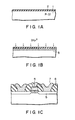
- the threshold voltage of a MOS transistor and, more particularly, of a D-type (Depletion) transistor is determined by the type and amount of an impurity used for the step of ion implantation in a channel, as shown in Figs. 1A to 1C.
- Fig. 1A shows a step of forming a gate insulating film 2 having a thickness of, e.g., 200 ⁇ on, e.g., a p-type semiconductor substrate 1.
- Fig. 1B shows a step of ion implantation in a channel for controlling the threshold voltage of a MOS transistor.
- Fig. 1A shows a step of forming a gate insulating film 2 having a thickness of, e.g., 200 ⁇ on, e.g., a p-type semiconductor substrate 1.
- Fig. 1B shows a step of ion implantation in a channel for controlling the threshold voltage of a MOS transistor.
- phosphorus ions 3 are implanted at an acceleration energy of 70 KeV to a concentration of about 1 x 1012 cm ⁇ 2 in order to form, e.g., a depletion-type transistor.
- Fig. 1C shows a step of forming a gate electrode 4 and source and drain diffusion layers 5. In this case, when n-type polysilicon is used as the material of the gate electrode 4, the threshold voltage of the transistor is about -2 V.
- Reference numeral 6 denotes an insulating film; and 7, an aluminum wiring layer.
- the present invention has been made in view of the above situation and has as its object to provide a semiconductor device having different threshold voltages in a plurality of MOS transistors, and a method of manufacturing the same with fewer steps than in a conventional method.
- a semiconductor device comprises a semiconductor substrate of one conductivity type, a MOS transistor, formed in the semiconductor substrate and having source and drain layers of a conductivity type opposite to that of the semiconductor substrate, and a well layer formed in the vicinity of a channel region of the MOS transistor to control a threshold voltage thereof, wherein the well layer has a substantially semi-circular section with a non-flat lower surface.
- a method of the present invention comprises the steps of forming a mask in which a mask pattern width of a portion corresponding to a mask opening diameter is equal to or less than twice the diffusion depth of a well layer, and implanting an impurity in a prospective channel portion of a MOS transistor of a semiconductor substrate by using the mask, thereby forming the well layer.
- a semiconductor device having a well formed in a semiconductor substrate by setting the width of a portion of a mask pattern, used for impurity implantation, that corresponds to an opening diameter to be equal to or less than twice the diffusion depth of a well layer, and gate electrodes formed to have the well layer as a channel region of a MOS transistor.
- the well formed in the above manner has a substantially semi-circular section to facilitate impurity concentration control in the surface of the substrate (in the conventional well, since the impurity is implanted through a portion of a mask pattern having a considerably larger width than in the present invention, the surface concentration is uniform and it is difficult to control the threshold voltage). Furthermore, since a plurality of types of opening patterns having a small mask pattern width are formed in a single mask, MOS transistors having different threshold voltages can be formed in a single process.
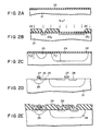
- a first thermal oxide film 22 is formed on a p-type substrate 21 having an impurity concentration of about 3 x 1015 cm ⁇ 3.
- a resist mask 23 having resist patterns of different opening widths (mask pattern widths) is formed on prospective depletion-type transistor regions, as shown in Fig. 2B.
- Phosphorus ions are implanted in the substrate 21 at a dose of about 7 x 1013 cm ⁇ 2 and an acceleration energy of 70 KeV.
- the structure is then annealed at 1,150°C for about 4 hours to diffuse the phosphorus.
- a depth X j1 of a diffusion layer 24 formed by phosphorus diffusion using a resist pattern 23 1 having a large width, e.g., 8 ⁇ m, is about 3 ⁇ m.
- the surface phosphorus concentration is about 3 x 1017 cm ⁇ 3.
- a depth X j2 of a well 25 formed by using a resist pattern 23 2 having a small width of 1 ⁇ m becomes 1 ⁇ m, and the surface concentration thereof is about 5 x 1016 cm ⁇ 3.
- MOS transistor gate electrodes 27 are formed at portions corresponding to the resist patterns 231 and 232.
- Source and drain diffusion layers 28 are formed by, e.g., ion implantation.
- an aluminum wiring layer 30 is formed over an insulating film 29 formed on the substrate as shown in Fig. 2E, thus completing MOS transistors.
- the well 24 shown in Figs. 2C to 2E is formed using the resist pattern 231 having a mask width greatly larger than twice its diffusion depth x j1 and corresponds to a conventional well.
- the well 25 is formed by using the resist pattern 232 having a mask width equal to or less than twice its diffusion depth X j2 .
- the well 25 has a substantially semi-circular section and is appropriate for threshold voltage control. This is because when a pattern opening diameter is small, the impurity concentration and the depth of a diffusion layer (especially that of an ion-implantation type) are determined by the pattern opening diameter. In this case, the length of the gate electrode on the well 25 in the channel lengthwise direction is also equal to or less than twice its well diffusion depth.
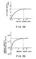
- Fig. 3A shows the resist space (opening pattern width) - diffusion depth characteristics of this embodiment
- Fig. 3B shows the resist space - diffusion layer surface impurity concentration characteristics of the same.
- the surface impurity concentration influences the threshold voltage of the MOS transistor.
- the threshold voltage can be changed in the positive direction (p-type impurity concentration is increased; n-type impurity concentration is decreased).
- the impurity concentration becomes identical to that of the p-type semiconductor substrate.
- Fig. 4A is a plan view of a pattern according to another embodiment of the present invention
- Fig. 4B is a sectional view taken along the line A - A' of Fig. 4A.
- the same reference numerals as in Figs. 2A to 2E denote the same or identical portions in Figs. 4A to 4B.
- a plurality of mask patterns 232 for impurity implantation are arranged on the channel regions of the MOS transistors.
- the diameter of each mask pattern 232 is equal to or less than twice its diffusion depth.
- a plurality of circular resist patterns 232 are formed in the channel regions of, e.g., MOS transistors, as shown in Fig. 4A. Phosphorus is implanted in these regions, and diffusion is subsequently performed to appropriately set the surface phosphorus concentration. As a result, the threshold voltages of the MOS transistors can be set.
- FIG. 5A is a plan view of a pattern of this example
- Fig. 5B is a sectional view taken along the line B - B of Fig. 5A.
- two mask patterns 232 for impurity implantation are arranged parallel to the channel widthwise direction of the MOS transistors.
- the condition of the pattern width being equal to or less than twice the diffusion depth must apply only to the widthwise direction (shorter direction) of the mask patterns 232, and need not apply to the lengthwise direction.
- Fig. 6 shows still another embodiment of the present invention.
- a well 25 as shown in Fig. 6 may be adopted.
- the well 25 must similarly satisfy the above condition (the width must be equal to or less than twice the diffusion depth).
- the shape of the mask pattern can be changed in various manners.
- the well is of a conductivity type opposite to that of the semiconductor substrate.
- the present invention can also be applied to an enhancement-type semiconductor device wherein the conductivity type of the well 25 is changed so that it will be of the same conductivity type as that of the substrate 21.
- the well has a "semi-circular" shape. However, it does not mean a true semi-circle but a shape whose bottom is not flat, unlike the well 24, but is curved, like the well 25.
- MOS transistors having different threshold voltages can be formed by the same manufacturing process (photoengraving steps) by forming a plurality of patterns having different opening diameters in a single mask, thus resulting in greatly simplified manufacturing steps.
Landscapes
- Metal-Oxide And Bipolar Metal-Oxide Semiconductor Integrated Circuits (AREA)
- Insulated Gate Type Field-Effect Transistor (AREA)
Applications Claiming Priority (2)
| Application Number | Priority Date | Filing Date | Title |
|---|---|---|---|
| JP104580/90 | 1990-04-20 | ||
| JP2104580A JP2809810B2 (ja) | 1990-04-20 | 1990-04-20 | 半導体装置の製造方法 |
Publications (2)
| Publication Number | Publication Date |
|---|---|
| EP0452817A1 true EP0452817A1 (fr) | 1991-10-23 |
| EP0452817B1 EP0452817B1 (fr) | 1995-10-11 |
Family
ID=14384375
Family Applications (1)
| Application Number | Title | Priority Date | Filing Date |
|---|---|---|---|
| EP91105804A Expired - Lifetime EP0452817B1 (fr) | 1990-04-20 | 1991-04-11 | Dispositif à semiconducteur avec des transistors MOS et procédé pour sa fabrication |
Country Status (4)
| Country | Link |
|---|---|
| EP (1) | EP0452817B1 (fr) |
| JP (1) | JP2809810B2 (fr) |
| KR (1) | KR940008357B1 (fr) |
| DE (1) | DE69113673T2 (fr) |
Cited By (8)
| Publication number | Priority date | Publication date | Assignee | Title |
|---|---|---|---|---|
| EP0915509A1 (fr) * | 1997-10-24 | 1999-05-12 | STMicroelectronics S.r.l. | Procédé d'intégration -dans le même puce semi-conductrice- de dispositifs semi-conducteurs comportant des tensions de seuil différentes |
| US7186623B2 (en) * | 2003-01-27 | 2007-03-06 | Renesas Technology Corp. | Integrated semiconductor device and method of manufacturing thereof |
| US7671425B2 (en) | 1998-02-05 | 2010-03-02 | Semiconductor Energy Laboratory Co., Ltd. | Semiconductor device and method of manufacturing the same |
| CN113363308A (zh) * | 2020-03-05 | 2021-09-07 | 上海先进半导体制造有限公司 | P沟道的沟槽型vdmos和沟槽型igbt |
| CN113363318A (zh) * | 2020-03-05 | 2021-09-07 | 上海先进半导体制造有限公司 | N沟道的平面型vdmos和平面型igbt |
| CN113363324A (zh) * | 2020-03-05 | 2021-09-07 | 上海先进半导体制造有限公司 | P沟道的平面型vdmos和平面型igbt |
| CN113363322A (zh) * | 2020-03-05 | 2021-09-07 | 上海先进半导体制造有限公司 | N沟道的沟槽型vdmos和沟槽型igbt |
| CN116230638A (zh) * | 2021-12-03 | 2023-06-06 | 立锜科技股份有限公司 | 耗尽型高压nmos元件与耗尽型低压nmos元件整合制造方法 |
Families Citing this family (5)
| Publication number | Priority date | Publication date | Assignee | Title |
|---|---|---|---|---|
| JP3367776B2 (ja) * | 1993-12-27 | 2003-01-20 | 株式会社東芝 | 半導体装置 |
| JP2003007723A (ja) * | 2001-06-26 | 2003-01-10 | Kitakyushu Foundation For The Advancement Of Industry Science & Technology | 半導体素子及び半導体集積回路 |
| JP4896699B2 (ja) * | 2006-12-21 | 2012-03-14 | 株式会社半導体エネルギー研究所 | 絶縁ゲイト型半導体装置およびその作製方法 |
| JP4628399B2 (ja) * | 2007-06-05 | 2011-02-09 | 株式会社半導体エネルギー研究所 | 半導体装置 |
| CN115274449A (zh) * | 2022-07-19 | 2022-11-01 | 华虹半导体(无锡)有限公司 | 耗尽型mos器件的制造方法 |
Family Cites Families (2)
| Publication number | Priority date | Publication date | Assignee | Title |
|---|---|---|---|---|
| JPS5120916B2 (fr) * | 1973-04-11 | 1976-06-29 | ||
| JPS52127181A (en) * | 1976-04-19 | 1977-10-25 | Nippon Telegr & Teleph Corp <Ntt> | Insulated gate type filed effect transistor |
-
1990
- 1990-04-20 JP JP2104580A patent/JP2809810B2/ja not_active Expired - Fee Related
-
1991
- 1991-04-11 EP EP91105804A patent/EP0452817B1/fr not_active Expired - Lifetime
- 1991-04-11 DE DE69113673T patent/DE69113673T2/de not_active Expired - Fee Related
- 1991-04-16 KR KR1019910006071A patent/KR940008357B1/ko not_active Expired - Fee Related
Non-Patent Citations (2)
| Title |
|---|
| I.E.E.E. TRANSACTIONS ON ELECTRON DEVICES, vol. ED-33, no. 3, March 1986, pages 426-428, New York, NY, US; R. STENGL et al.: "Variation of Lateral Doping as a Field Terminator for High-Voltage Power Devices" * |
| PATENT ABSTRACTS OF JAPAN, vol. 11, no. 174 (E-513)[2621] 4 June 1987; & JP-A-62 008 553 (TOSHIBA) 16.01.1987 * |
Cited By (13)
| Publication number | Priority date | Publication date | Assignee | Title |
|---|---|---|---|---|
| EP0915509A1 (fr) * | 1997-10-24 | 1999-05-12 | STMicroelectronics S.r.l. | Procédé d'intégration -dans le même puce semi-conductrice- de dispositifs semi-conducteurs comportant des tensions de seuil différentes |
| US7671425B2 (en) | 1998-02-05 | 2010-03-02 | Semiconductor Energy Laboratory Co., Ltd. | Semiconductor device and method of manufacturing the same |
| US7186623B2 (en) * | 2003-01-27 | 2007-03-06 | Renesas Technology Corp. | Integrated semiconductor device and method of manufacturing thereof |
| US7541248B2 (en) | 2003-01-27 | 2009-06-02 | Renesas Technology Corp. | Integrated semiconductor device and method of manufacturing thereof |
| CN113363324A (zh) * | 2020-03-05 | 2021-09-07 | 上海先进半导体制造有限公司 | P沟道的平面型vdmos和平面型igbt |
| CN113363318A (zh) * | 2020-03-05 | 2021-09-07 | 上海先进半导体制造有限公司 | N沟道的平面型vdmos和平面型igbt |
| CN113363308A (zh) * | 2020-03-05 | 2021-09-07 | 上海先进半导体制造有限公司 | P沟道的沟槽型vdmos和沟槽型igbt |
| CN113363322A (zh) * | 2020-03-05 | 2021-09-07 | 上海先进半导体制造有限公司 | N沟道的沟槽型vdmos和沟槽型igbt |
| CN113363318B (zh) * | 2020-03-05 | 2023-12-08 | 上海积塔半导体有限公司 | N沟道的平面型vdmos和平面型igbt |
| CN113363322B (zh) * | 2020-03-05 | 2023-12-08 | 上海积塔半导体有限公司 | N沟道的沟槽型vdmos和沟槽型igbt |
| CN113363324B (zh) * | 2020-03-05 | 2024-01-30 | 上海积塔半导体有限公司 | P沟道的平面型vdmos和平面型igbt |
| CN113363308B (zh) * | 2020-03-05 | 2024-03-15 | 上海积塔半导体有限公司 | P沟道的沟槽型vdmos和沟槽型igbt |
| CN116230638A (zh) * | 2021-12-03 | 2023-06-06 | 立锜科技股份有限公司 | 耗尽型高压nmos元件与耗尽型低压nmos元件整合制造方法 |
Also Published As
| Publication number | Publication date |
|---|---|
| JPH043468A (ja) | 1992-01-08 |
| JP2809810B2 (ja) | 1998-10-15 |
| KR940008357B1 (ko) | 1994-09-12 |
| DE69113673D1 (de) | 1995-11-16 |
| DE69113673T2 (de) | 1996-04-18 |
| EP0452817B1 (fr) | 1995-10-11 |
Similar Documents
| Publication | Publication Date | Title |
|---|---|---|
| US5210437A (en) | MOS device having a well layer for controlling threshold voltage | |
| US5548143A (en) | Metal oxide semiconductor transistor and a method for manufacturing the same | |
| US5917218A (en) | Peripheral circuits including high voltage transistors with LDD structures for nonvolatile memories | |
| US6071775A (en) | Methods for forming peripheral circuits including high voltage transistors with LDD structures | |
| EP0452817B1 (fr) | Dispositif à semiconducteur avec des transistors MOS et procédé pour sa fabrication | |
| US4535532A (en) | Integrated circuit contact technique | |
| US4806500A (en) | Method of producing a large-scale integrated MOS field-effect transistor circuit | |
| KR0149659B1 (ko) | 반도체 장치 및 그 제조방법 | |
| US5212542A (en) | Semiconductor device having at least two field effect transistors and method of manufacturing the same | |
| EP0683531B1 (fr) | MOSFET avec une structure LDD et sa méthode de fabrication | |
| US6713331B2 (en) | Semiconductor device manufacturing using one element separation film | |
| US5273914A (en) | Method of fabricating a CMOS semiconductor devices | |
| US5266508A (en) | Process for manufacturing semiconductor device | |
| US6228697B1 (en) | Method of manufacturing semiconductor device including field effect transistors | |
| KR0166991B1 (ko) | 반도체 장치 | |
| KR980006533A (ko) | 반도체 장치 및 그 제조방법 | |
| KR940005291B1 (ko) | 불순물 편석현상을 이용한 반도체장치의 제조방법 | |
| EP0421446B1 (fr) | Dispositif semi-conducteur comprenant un MOSFET à canal N, un MOSFET à canal P et une cellule de mémoire non-volatile formés dans une puce | |
| JPS62265765A (ja) | 半導体装置の製造方法 | |
| JP2595058B2 (ja) | 不揮発性半導体記憶装置の製造方法 | |
| KR100431324B1 (ko) | 반도체장치의 제조방법 | |
| JP2880885B2 (ja) | 半導体集積回路装置及びその製造方法 | |
| KR100371284B1 (ko) | 플랫 셀형 반도체 메모리 장치의 제조 방법 | |
| KR0147649B1 (ko) | 불휘발성 반도체 메모리 장치 제조방법 | |
| EP0313777A2 (fr) | Procédé pour augmenter la densité de concentration de dopants dans des régions sélectionnées de dispositifs semi-conducteurs |
Legal Events
| Date | Code | Title | Description |
|---|---|---|---|
| PUAI | Public reference made under article 153(3) epc to a published international application that has entered the european phase |
Free format text: ORIGINAL CODE: 0009012 |
|
| 17P | Request for examination filed |
Effective date: 19910411 |
|
| AK | Designated contracting states |
Kind code of ref document: A1 Designated state(s): DE FR GB |
|
| 17Q | First examination report despatched |
Effective date: 19940325 |
|
| GRAA | (expected) grant |
Free format text: ORIGINAL CODE: 0009210 |
|
| AK | Designated contracting states |
Kind code of ref document: B1 Designated state(s): DE FR GB |
|
| REF | Corresponds to: |
Ref document number: 69113673 Country of ref document: DE Date of ref document: 19951116 |
|
| ET | Fr: translation filed | ||
| PLBE | No opposition filed within time limit |
Free format text: ORIGINAL CODE: 0009261 |
|
| STAA | Information on the status of an ep patent application or granted ep patent |
Free format text: STATUS: NO OPPOSITION FILED WITHIN TIME LIMIT |
|
| 26N | No opposition filed | ||
| PGFP | Annual fee paid to national office [announced via postgrant information from national office to epo] |
Ref country code: FR Payment date: 19970409 Year of fee payment: 7 |
|
| PGFP | Annual fee paid to national office [announced via postgrant information from national office to epo] |
Ref country code: DE Payment date: 19970418 Year of fee payment: 7 |
|
| K1C1 | Correction of patent application (title page) published |
Effective date: 19911023 |
|
| PG25 | Lapsed in a contracting state [announced via postgrant information from national office to epo] |
Ref country code: FR Free format text: THE PATENT HAS BEEN ANNULLED BY A DECISION OF A NATIONAL AUTHORITY Effective date: 19980430 |
|
| REG | Reference to a national code |
Ref country code: GB Ref legal event code: 746 Effective date: 19981010 |
|
| PG25 | Lapsed in a contracting state [announced via postgrant information from national office to epo] |
Ref country code: DE Free format text: LAPSE BECAUSE OF NON-PAYMENT OF DUE FEES Effective date: 19990202 |
|
| REG | Reference to a national code |
Ref country code: FR Ref legal event code: ST |
|
| REG | Reference to a national code |
Ref country code: GB Ref legal event code: IF02 |
|
| PGFP | Annual fee paid to national office [announced via postgrant information from national office to epo] |
Ref country code: GB Payment date: 20060405 Year of fee payment: 16 |
|
| GBPC | Gb: european patent ceased through non-payment of renewal fee |
Effective date: 20070411 |
|
| PG25 | Lapsed in a contracting state [announced via postgrant information from national office to epo] |
Ref country code: GB Free format text: LAPSE BECAUSE OF NON-PAYMENT OF DUE FEES Effective date: 20070411 |