EP0452869A1 - Verfahren zur Herstellung einer Halbleiter-Vorrichtung - Google Patents
Verfahren zur Herstellung einer Halbleiter-Vorrichtung Download PDFInfo
- Publication number
- EP0452869A1 EP0452869A1 EP91106033A EP91106033A EP0452869A1 EP 0452869 A1 EP0452869 A1 EP 0452869A1 EP 91106033 A EP91106033 A EP 91106033A EP 91106033 A EP91106033 A EP 91106033A EP 0452869 A1 EP0452869 A1 EP 0452869A1
- Authority
- EP
- European Patent Office
- Prior art keywords
- layer
- substrate
- algaas
- doped
- gaas
- Prior art date
- Legal status (The legal status is an assumption and is not a legal conclusion. Google has not performed a legal analysis and makes no representation as to the accuracy of the status listed.)
- Ceased
Links
Images


Classifications
-
- B—PERFORMING OPERATIONS; TRANSPORTING
- B82—NANOTECHNOLOGY
- B82Y—SPECIFIC USES OR APPLICATIONS OF NANOSTRUCTURES; MEASUREMENT OR ANALYSIS OF NANOSTRUCTURES; MANUFACTURE OR TREATMENT OF NANOSTRUCTURES
- B82Y20/00—Nanooptics, e.g. quantum optics or photonic crystals
-
- H—ELECTRICITY
- H01—ELECTRIC ELEMENTS
- H01S—DEVICES USING THE PROCESS OF LIGHT AMPLIFICATION BY STIMULATED EMISSION OF RADIATION [LASER] TO AMPLIFY OR GENERATE LIGHT; DEVICES USING STIMULATED EMISSION OF ELECTROMAGNETIC RADIATION IN WAVE RANGES OTHER THAN OPTICAL
- H01S5/00—Semiconductor lasers
- H01S5/30—Structure or shape of the active region; Materials used for the active region
- H01S5/32—Structure or shape of the active region; Materials used for the active region comprising PN junctions, e.g. hetero- or double- heterostructures
- H01S5/323—Structure or shape of the active region; Materials used for the active region comprising PN junctions, e.g. hetero- or double- heterostructures in AIIIBV compounds, e.g. AlGaAs-laser, InP-based laser
- H01S5/32308—Structure or shape of the active region; Materials used for the active region comprising PN junctions, e.g. hetero- or double- heterostructures in AIIIBV compounds, e.g. AlGaAs-laser, InP-based laser emitting light at a wavelength less than 900 nm
-
- H—ELECTRICITY
- H01—ELECTRIC ELEMENTS
- H01S—DEVICES USING THE PROCESS OF LIGHT AMPLIFICATION BY STIMULATED EMISSION OF RADIATION [LASER] TO AMPLIFY OR GENERATE LIGHT; DEVICES USING STIMULATED EMISSION OF ELECTROMAGNETIC RADIATION IN WAVE RANGES OTHER THAN OPTICAL
- H01S5/00—Semiconductor lasers
- H01S5/30—Structure or shape of the active region; Materials used for the active region
- H01S5/34—Structure or shape of the active region; Materials used for the active region comprising quantum well or superlattice structures, e.g. single quantum well [SQW] lasers, multiple quantum well [MQW] lasers or graded index separate confinement heterostructure [GRINSCH] lasers
- H01S5/343—Structure or shape of the active region; Materials used for the active region comprising quantum well or superlattice structures, e.g. single quantum well [SQW] lasers, multiple quantum well [MQW] lasers or graded index separate confinement heterostructure [GRINSCH] lasers in AIIIBV compounds, e.g. AlGaAs-laser, InP-based laser
- H01S5/34313—Structure or shape of the active region; Materials used for the active region comprising quantum well or superlattice structures, e.g. single quantum well [SQW] lasers, multiple quantum well [MQW] lasers or graded index separate confinement heterostructure [GRINSCH] lasers in AIIIBV compounds, e.g. AlGaAs-laser, InP-based laser with a well layer having only As as V-compound, e.g. AlGaAs, InGaAs
-
- H—ELECTRICITY
- H10—SEMICONDUCTOR DEVICES; ELECTRIC SOLID-STATE DEVICES NOT OTHERWISE PROVIDED FOR
- H10D—INORGANIC ELECTRIC SEMICONDUCTOR DEVICES
- H10D30/00—Field-effect transistors [FET]
- H10D30/40—FETs having zero-dimensional [0D], one-dimensional [1D] or two-dimensional [2D] charge carrier gas channels
- H10D30/47—FETs having zero-dimensional [0D], one-dimensional [1D] or two-dimensional [2D] charge carrier gas channels having two-dimensional [2D] charge carrier gas channels, e.g. nanoribbon FETs or high electron mobility transistors [HEMT]
- H10D30/471—High electron mobility transistors [HEMT] or high hole mobility transistors [HHMT]
- H10D30/473—High electron mobility transistors [HEMT] or high hole mobility transistors [HHMT] having confinement of carriers by multiple heterojunctions, e.g. quantum well HEMT
- H10D30/4732—High electron mobility transistors [HEMT] or high hole mobility transistors [HHMT] having confinement of carriers by multiple heterojunctions, e.g. quantum well HEMT using Group III-V semiconductor material
-
- H—ELECTRICITY
- H10—SEMICONDUCTOR DEVICES; ELECTRIC SOLID-STATE DEVICES NOT OTHERWISE PROVIDED FOR
- H10D—INORGANIC ELECTRIC SEMICONDUCTOR DEVICES
- H10D62/00—Semiconductor bodies, or regions thereof, of devices having potential barriers
- H10D62/10—Shapes, relative sizes or dispositions of the regions of the semiconductor bodies; Shapes of the semiconductor bodies
- H10D62/17—Semiconductor regions connected to electrodes not carrying current to be rectified, amplified or switched, e.g. channel regions
- H10D62/351—Substrate regions of field-effect devices
- H10D62/357—Substrate regions of field-effect devices of FETs
-
- H—ELECTRICITY
- H10—SEMICONDUCTOR DEVICES; ELECTRIC SOLID-STATE DEVICES NOT OTHERWISE PROVIDED FOR
- H10H—INORGANIC LIGHT-EMITTING SEMICONDUCTOR DEVICES HAVING POTENTIAL BARRIERS
- H10H20/00—Individual inorganic light-emitting semiconductor devices having potential barriers, e.g. light-emitting diodes [LED]
- H10H20/01—Manufacture or treatment
- H10H20/011—Manufacture or treatment of bodies, e.g. forming semiconductor layers
- H10H20/013—Manufacture or treatment of bodies, e.g. forming semiconductor layers having light-emitting regions comprising only Group III-V materials
-
- H—ELECTRICITY
- H10—SEMICONDUCTOR DEVICES; ELECTRIC SOLID-STATE DEVICES NOT OTHERWISE PROVIDED FOR
- H10P—GENERIC PROCESSES OR APPARATUS FOR THE MANUFACTURE OR TREATMENT OF DEVICES COVERED BY CLASS H10
- H10P14/00—Formation of materials, e.g. in the shape of layers or pillars
- H10P14/20—Formation of materials, e.g. in the shape of layers or pillars of semiconductor materials
- H10P14/29—Formation of materials, e.g. in the shape of layers or pillars of semiconductor materials characterised by the substrates
- H10P14/2901—Materials
- H10P14/2902—Materials being Group IVA materials
- H10P14/2905—Silicon, silicon germanium or germanium
-
- H—ELECTRICITY
- H10—SEMICONDUCTOR DEVICES; ELECTRIC SOLID-STATE DEVICES NOT OTHERWISE PROVIDED FOR
- H10P—GENERIC PROCESSES OR APPARATUS FOR THE MANUFACTURE OR TREATMENT OF DEVICES COVERED BY CLASS H10
- H10P14/00—Formation of materials, e.g. in the shape of layers or pillars
- H10P14/20—Formation of materials, e.g. in the shape of layers or pillars of semiconductor materials
- H10P14/29—Formation of materials, e.g. in the shape of layers or pillars of semiconductor materials characterised by the substrates
- H10P14/2901—Materials
- H10P14/2907—Materials being Group IIIA-VA materials
- H10P14/2911—Arsenides
-
- H—ELECTRICITY
- H10—SEMICONDUCTOR DEVICES; ELECTRIC SOLID-STATE DEVICES NOT OTHERWISE PROVIDED FOR
- H10P—GENERIC PROCESSES OR APPARATUS FOR THE MANUFACTURE OR TREATMENT OF DEVICES COVERED BY CLASS H10
- H10P14/00—Formation of materials, e.g. in the shape of layers or pillars
- H10P14/20—Formation of materials, e.g. in the shape of layers or pillars of semiconductor materials
- H10P14/32—Formation of materials, e.g. in the shape of layers or pillars of semiconductor materials characterised by intermediate layers between substrates and deposited layers
- H10P14/3202—Materials thereof
- H10P14/3214—Materials thereof being Group IIIA-VA semiconductors
- H10P14/3221—Arsenides
-
- H—ELECTRICITY
- H10—SEMICONDUCTOR DEVICES; ELECTRIC SOLID-STATE DEVICES NOT OTHERWISE PROVIDED FOR
- H10P—GENERIC PROCESSES OR APPARATUS FOR THE MANUFACTURE OR TREATMENT OF DEVICES COVERED BY CLASS H10
- H10P14/00—Formation of materials, e.g. in the shape of layers or pillars
- H10P14/20—Formation of materials, e.g. in the shape of layers or pillars of semiconductor materials
- H10P14/34—Deposited materials, e.g. layers
- H10P14/3402—Deposited materials, e.g. layers characterised by the chemical composition
- H10P14/3414—Deposited materials, e.g. layers characterised by the chemical composition being group IIIA-VIA materials
- H10P14/3421—Arsenides
-
- H—ELECTRICITY
- H10—SEMICONDUCTOR DEVICES; ELECTRIC SOLID-STATE DEVICES NOT OTHERWISE PROVIDED FOR
- H10P—GENERIC PROCESSES OR APPARATUS FOR THE MANUFACTURE OR TREATMENT OF DEVICES COVERED BY CLASS H10
- H10P14/00—Formation of materials, e.g. in the shape of layers or pillars
- H10P14/20—Formation of materials, e.g. in the shape of layers or pillars of semiconductor materials
- H10P14/34—Deposited materials, e.g. layers
- H10P14/3438—Doping during depositing
- H10P14/3441—Conductivity type
- H10P14/3444—P-type
-
- H—ELECTRICITY
- H01—ELECTRIC ELEMENTS
- H01S—DEVICES USING THE PROCESS OF LIGHT AMPLIFICATION BY STIMULATED EMISSION OF RADIATION [LASER] TO AMPLIFY OR GENERATE LIGHT; DEVICES USING STIMULATED EMISSION OF ELECTROMAGNETIC RADIATION IN WAVE RANGES OTHER THAN OPTICAL
- H01S5/00—Semiconductor lasers
- H01S5/30—Structure or shape of the active region; Materials used for the active region
- H01S5/34—Structure or shape of the active region; Materials used for the active region comprising quantum well or superlattice structures, e.g. single quantum well [SQW] lasers, multiple quantum well [MQW] lasers or graded index separate confinement heterostructure [GRINSCH] lasers
- H01S5/343—Structure or shape of the active region; Materials used for the active region comprising quantum well or superlattice structures, e.g. single quantum well [SQW] lasers, multiple quantum well [MQW] lasers or graded index separate confinement heterostructure [GRINSCH] lasers in AIIIBV compounds, e.g. AlGaAs-laser, InP-based laser
- H01S5/34313—Structure or shape of the active region; Materials used for the active region comprising quantum well or superlattice structures, e.g. single quantum well [SQW] lasers, multiple quantum well [MQW] lasers or graded index separate confinement heterostructure [GRINSCH] lasers in AIIIBV compounds, e.g. AlGaAs-laser, InP-based laser with a well layer having only As as V-compound, e.g. AlGaAs, InGaAs
- H01S5/3432—Structure or shape of the active region; Materials used for the active region comprising quantum well or superlattice structures, e.g. single quantum well [SQW] lasers, multiple quantum well [MQW] lasers or graded index separate confinement heterostructure [GRINSCH] lasers in AIIIBV compounds, e.g. AlGaAs-laser, InP-based laser with a well layer having only As as V-compound, e.g. AlGaAs, InGaAs the whole junction comprising only (AI)GaAs
Definitions
- This invention relates to a semiconductor device such as a semiconductor laser or a field effect type transistor (FET) and a method of making the same, and particularly to a semiconductor device comprising a substrate and a plurality of semiconductor layers of GaAs or AlGaAs formed thereon, and a method of making the same.
- a semiconductor device such as a semiconductor laser or a field effect type transistor (FET) and a method of making the same, and particularly to a semiconductor device comprising a substrate and a plurality of semiconductor layers of GaAs or AlGaAs formed thereon, and a method of making the same.
- FET field effect type transistor
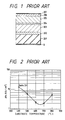
- FIG. 1 of the accompanying drawings is a schematic cross-sectional view showing an example of such a prior-art semiconductor laser.
- Figure 2 of the accompanying drawings shows the relation between the threshold value current density Jth in the semiconductor laser of Figure 1 and the substrate temperature during making.
- the reference numeral 201 designates an n-GaAs substrate
- the reference numeral 202 denotes an Si-doped GaAs layer having a thickness of 0.5 ⁇ m which is a buffer layer
- the reference numeral 203 designates an Si-doped Al 0.3 Ga 0.7 As clad layer having a thickness of 1.5 ⁇ m
- the reference numeral 204 denotes an active layer having a thickness of 1 ⁇ m formed of undoped GaAs
- the reference numeral 205 designates a Be-doped Al 0.3 Ga 0.7 As clad layer having a thickness of 5 ⁇ m
- the reference numeral 206 denotes a Be-doped GaAs layer which is a contact layer having a thickness of 0.5 ⁇ m
- the reference numeral 207 designates a Cr/Au alloy electrode deposited on the contact layer 206
- the reference numeral 208 denotes an AuGe/Ni/Au electrode deposited on the back of the substrate after the
- OEIC integrated circuit
- MBE Very Low Threshold Current GaAs-AlGaAs GRINSCH Lasers Grown by MBE for OEIC Applications.
- OEIC has characteristics such as improved reliability, reduced cost and compactness and is regarded as an important technique, but a problem which arises when it is integrated is the temperature of manufacture.
- the problem is that according to the conventional manner, the temperature of manufacture when the device is made, i.e., the substrate temperature, is hight and therefore the mutual diffusion of constituent elements and impurities occurs and an ideal doping profile (distribution) and ideal structure cannot be made.
- Optical devices such as semiconductor lasers are made usually at 600°C or higher as previously described and nowadays, they are made at higher temperatures of the order of 700°C for the purposed of improving the performance thereof.
- electrical devices are made chiefly at a growth temperature in the vicinity of 500°C because they are apt to easily suffer from the mutual diffusion or the like of impurities. That is, here is already given birth to a temperature difference of the order of 200°C.
- the electrical device is made always after an optical device is made. Consequently, a plurality of epitaxial grows differing in structure becomes impossible.
- low-temperature growth is a very important technique in the semiconductor process, and is particularly the low-temperature growth of a semiconductor laser which provides the center of an optical device is important to the technique of integrating an optical device and an electrical device.
- GaAs/Ge/Si structure with Ge as an intermediate layer
- a two-step growing method of cleaning an Si substrate at a high temperature, and thereafter growing amorphous thin GaAs at a low temperature, and increasing the temperature and growing GaAs at the ordinary growth temperature that is, the structure is GaAs/low temperature GaAs/Si
- a method of growing GaAs/AlGaAs super-lattice on Si and growing GaAs thereon the structure is GaAs/GaAs-AlGaAs super-lattice/Si
- a method of making an intermediate layer into a strain super-lattice (GaAs/strain super-lattice/Si).
- Any of these growing methods uses MBE or organic metal chemical vapor phase deposition (MOCVD), and obtains single crystal of GaAs.
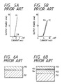
- Figure 4 is a schematic perspective view showing another example of the prior-art semiconductor laser.
- a normal pressure MOCVD apparatus was used and an n type Si substrate 171 of (100) 2° off was used to form a GaP layer 172 with a thickness of 0.1 ⁇ m on the Si substrate 171 at 900°C, and a GaP/GaAsP strain super-lattice (20 nm/20 nm x 5) 173 was formed at 750°C, and a GaAsP/GaAs strain super-lattice (20 nm/20 nm x 5) 173 was further formed, and on this super-lattice structure (SLS) 173, there were successively grown an n-GaAs layer 174 (having a thickness of 2 ⁇ m and impurity concentration of 2 x 1018 cm ⁇ 3), an n-Al x Ga 1-x As layer 175 (having a thickness of 1.4 ⁇ m and impurity concentration of 1 x 1018 cm ⁇ 3) which
- an AuZn/Au layer 180 was deposited as an electrode on P side and an AuSb/Au layer 181 was deposited as an electrode on n side to make a laser of 10 ⁇ m wide stripe having a cavity length of about 300 ⁇ m.
- Figure 5A shows the characteristic of a laser made on a GaAs substrate
- Figure 5B shows the characteristic of the laser made on the Si substrate as described above. It is seen that in the DH (double hetero) laser on GaAs, oscillation takes place only in the TE mode, while in the laser on Si, oscillation takes place in the TE + TM mode and the TM mode. This is considered to be attributable to the fact that Si and GaAs differ in coefficient of thermal expansion and therefore the GaAs layer grown on Si is subjected to a stress of about 109 dyn/cm2 and a light hole level and a heavy hole level have separated from each other.
- GaAs substrate may generally be mentioned as the substrate.
- AlGaAs and GaP substantially coincide with GaAs in lattice constant, and light emitting diodes and semiconductor lasers using these materials have already been put into practical use.
- light emitting diodes and semiconductor lasers using ZnSe have not yet been put into practical use. This is because the doping of ZnSe is difficult and because the growth temperatures of ZnSe film and GaAs film differ greatly from each other.
- the optimum growth condition of ZnSe is 250°C - 350°C, whereas the optimum growth condition of GaAs is 500°C or higher.
- Figures 6A and 6B of the accompanying drawings show an example of this.
- an n-ZnSe layer 152 is grown on a substrate 151 of n-GaAs.
- the growth temperature at this time is 300°C.
- an n type GaAs layer 153 is grown at a growth temperature of 500°C.
- Zn diffuses from the ZnSe layer 152 into the GaAs layer 153 with the result that some area 155 of the GaAs layer 153 becomes a P type GaAs area.
- Ga diffuses from the GaAs layer 153 into the ZnSe layer 152 and an n area indicated by 154 is formed in the ZnSe layer 152.
- npn junction is formed between the substrate 151 and the GaAs layer 153.
- a light emitting device including a ZnSe layer and the integration of GaAs, ZnSe, GaP, etc. can be achieved and further, this will provide an important technique of growth of crystal of II-VI group which is generally low in growth temperature.
- a semiconductor device which comprises a plurality of semiconductor layers formed on a substrate and including an active layer and formed of one of GaAs and AlGaAs and in which a GaAs layer having a thickness exceeding 500 ⁇ is not interposed between the substrate and the active layer.
- a semiconductor laser which is an embodiment of the present invention comprises: a substrate; a buffer layer formed on said substrate and formed of AlGaAs; a first clad layer formed on said buffer layer and formed of AlGaAs; a first light confining layer formed on said first clad layer and formed of AlGaAs; an active layer formed on said first light confining layer; a second light confining layer formed on said active layer; a second clad layer formed on said second light confining layer; and an electrode for letting an electric current flow to said active layer.
- a high electron mobility transistor which is another embodiment of the present invention comprises: a substrate; a buffer layer formed on said substrate and formed of AlGaAs; an active layer formed on said buffer layer; a doped layer formed on said active layer and formed of a semiconductor doped with impurities, a two-dimensional electron gas layer being formed on the interface between said doped layer and said active layer; and source, gate and drain electrodes formed on said doped layer.
- a method of making the semiconductor device according to the present invention as described above comprises the steps of: setting the temperature of said substrate to 500°C or lower and growing on said substrate a semiconductor layer formed of AlGaAs; and setting the temperature of said substrate to 500°C or lower and growing an active layer on said AlGaAs layer without interposing a GaAs layer having a thickness exceeding 500 ⁇ between said substrate and said AlGaAs layer.
- Figure 1 is a schematic cross-sectional view showing an example of the semiconductor laser according to the prior art.
- Figure 2 is a graph showing the relation between the temperature of a substrate when the semiconductor laser of Figure 1 is made and the threshold value current of the laser made.
- Figure 3 is a graph showing the density distribution of a donor when Sn is diffused in a GaAs layer.
- Figure 4 is a schematic perspective view showing another example of the semiconductor laser according to the prior art.
- Figure 5A is a graph showing the current-output characteristic of a prior-art semiconductor laser using a GaAs substrate.
- Figure 5B is a graph showing the current-output characteristic of a prior-art semiconductor laser using an Si substrate.
- Figure 6A is a schematic cross-sectional view showing an example in which an n type ZnSe layer was grown on an n type GaAs substrate.
- Figure 6B is a schematic cross-sectional view showing an example in which an n type GaAs layer was further grown on the ZnSe layer of Figure 6.
- Figure 7 is a schematic cross-sectional view showing a semiconductor laser which is a first embodiment of the present invention.
- Figure 8 is a graph showing the relation between the temperature of a substrate and the intensity of the luminescence of each layer when a GaAs layer and an AlGaAs layer were grown on the substrate.
- Figure 9 is a graph showing the relation between the temperature of a substrate and threshold value current density when a semiconductor laser having an AlGaAs buffer layer is made.
- Figure 10 is a schematic cross-sectional view showing a semiconductor laser which is a second embodiment of the present invention.
- Figure 11 illustrates the multiplex quantum well structure of the semiconductor laser of Figure 10.
- Figure 12 is a schematic cross-sectional view showing a high electron mobility transistor which is a third embodiment of the present invention.
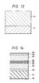
- Figure 13 is a schematic cross-sectional view showing an example in which a GaAs:Si layer was grown on an Si substrate.
- Figure 14 is a schematic cross-sectional view showing a semiconductor laser which is a fourth embodiment of the present invention.
- Figure 15 is a graph showing the relation between the temperature of a substrate and threshold value current density when a semiconductor laser having a buffer layer formed of GaAs or AlGaAs is made.
- Figure 16 is a schematic cross-sectional view showing a semiconductor laser which is a seventh embodiment of the present invention.
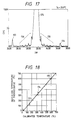
- Figure 17 is a graph showing the result of the X-ray diffraction measurement of an AlGaAs layer of periodic structure.
- Figure 18 is a graph showing the relation between the calibrated temperature of a molecular beam epitaxy device and the indication temperature of a thermocouple.
- Figure 7 is a schematic cross-sectional view showing a semiconductor laser which is a first embodiment of the present invention.
- an Al 0.2 Ga 0.8 As layer is used in place of the GaAs layer 202 which is the buffer layer according to the prior art.
- Figure 8 shows the substrate temperature dependency of the intensity of photoluminescence (PL) at 77K of undoped GaAs and Al 0.3 Ga 0.7 As made at a low growth temperature made by the BBE method.
- the ordinate represents the intensity of photoluminescence
- the abscissa represents the temperature of a substrate.
- Film of GaAs is greatest in the intensity of photoluminescence for the vicinity of 500°C as indicated by 13, and Al 0.3 Ga 0.7 As is greatest in the intensity of photoluminescence for the vicinity of 450°C as indicated by 14.
- the intensity of photoluminescence of GaAs sharply drops at 450°C or lower and GaAs does not shine at 400°C.
- Al 0.3 Ga 0.7 As does not sharply drop in the intensity of photoluminescence even if the temperature becomes 450°C or lower, and maintains the order of 1/3 of the intensity at 500°C even if the temperature becomes 300°C.
- the reference numeral 1 designates an n-GaAs substrate
- the reference numeral 2 denotes an n type buffer layer comprising Si-doped Al 0.2 Ga 0.8 As having a thickness of 0.5 ⁇ m
- the reference numeral 3 designates a clad layer comprising Si-doped Al 0.5 Ga 0.5 As having a thickness of 1.5 ⁇ m
- the reference numeral 5 designates a single quantum well (SQW) layer of GaAs which is an active layer having a thickness of 100 ⁇
- the reference numeral 7 designates
- AlGaAs buffer layer is inserted is lower in Jth is considered to be that at low temperatures (500°C or lower), AlGaAs is better in quality of crystal than GaAs and is particularly excellent in flatness.
- the GaAs layer should preferably be made as thin as possible or be eliminated to improve flatness.
- the GaAs layer is a super-lattice having a thickness of 500 ⁇ , it does not affect the characteristic of a device such as a laser.
- the periodic structure of a super-lattice for example, GaAs/AlGaAs, improves the characteristic of a laser.
- the thickness of one layer is 500 ⁇ or less, a plurality of GaAs layers may be included even where low-temperature growth is done.
- GaAs 500 ⁇ or less will now be described. If GaAs is pure, there will be no problem, but actually, GaAs sometimes contain more or less impurities such as Al and In. To realize the above-described effect (the improvement in the characteristic in low-temperature growth), these impurities must be limited, but the limit of impurities may be 0.1% or less as composition. However, the dopant which determines the n or p type conductivity is outside this limiting range. The purity of GaAs also applies to the following embodiments.
- FIG 10 is a schematic cross-sectional view of a semiconductor laser which is a second embodiment of the present invention.
- an active layer is of multiplex quantum well (MQW) structure.
- the reference numeral 41 designates a p-GaAs substrate
- the reference numeral 42 denotes a Be-doped Al 0.1 Ga 0.9 As layer which is a p type buffer layer having a thickness of 1.0 ⁇ m
- the reference numeral 43 designates a Be-doped Al 0.7 Ga 0.3 As layer which is a p type clad layer having a thickness of 1.5 ⁇ m
- the reference numeral 44 denotes a Be-doped Al 0.3 Ga 0.7 As layer (in which carrier concentration is 5 x 1017 cm ⁇ 3) which is a p type light confining layer having a thickness of 2000 ⁇
- the reference numeral 45 designates an MQW layer which is an active layer.
- the construction of the MQW layer 45 is shown in Figure 11.
- An undoped Al 0.1 Ga 0.9 As layer 51 having a thickness of 80 ⁇ is first formed as a well layer on the light confining layer 44, and an undoped Al 0.3 Ga 0.7 As layer having a thickness of 100 ⁇ is next formed as a barrier layer.
- Such layers 51 and 52 are alternately laminated and an Si-doped Al 0.3 Ga 0.7 As layer 46 which is an n type upper light confining layer is grown to 2000 ⁇ on the fifth well layer 51.
- the carrier concentration of the layer 46 is 5 x 1017 cm ⁇ 3.
- the upper arrow in Figure 11 indicates the lamination direction, and the numbers on the right side of Figure 11 indicate Al contents corresponding to band energy levels.
- an Si-doped Al 0.7 Ga 0.3 As layer 47 which is an n type upper clad layer is further formed to a thickness of 1.5 ⁇ m on the upper light confining layer 46.
- the carrier concentration of this layer 47 is 1 x 1018 cm ⁇ 3.
- An Si-doped GaAs layer 48 which is an n type cap layer is formed to a thickness of 0.5 ⁇ m on the layer 47 to provide laser structure.
- the reference numeral 49 designates an Au (5000 ⁇ )/Cr (500 ⁇ ) layer which is an n type electrode
- the reference numeral 50 denotes an Au (5000 ⁇ )/AuGe (2000 ⁇ ) layer which is a p type electrode.
- the electrodes 49 and 50 are deposited by evaporation and heat-treated.
- a super-lattice layer comprising a GaAs layer (150 ⁇ ) and an Al 0.1 Ga 0.9 As layer alternately laminated over five periods is included between the buffer layer 42 of Be-doped Al 0.1 Ga 0.9 As and the clad layer 43 of Be-doped Al 0.1 Ga 0.9 As.
- Figure 12 illustrates a third embodiment of the present invention.
- the reference numeral 81 designates a semi-insulative GaAs substrate
- the reference numeral 82 denotes an undoped Al 0.5 Ga 0.5 As layer which is a buffer layer having a thickness of 1.5 ⁇ m
- the reference numeral 83 designates an undoped GaAs layer which provides an active layer area having a thickness of 1 ⁇ m
- the reference numeral 84 denotes an Si-doped Al 0.2 Ga 0.8 As layer having a thickness of 0.5 ⁇ m
- the reference numeral 85 designates a source electrode
- the reference numeral 86 denotes a gate electrode
- the reference numeral 87 designates a drain electrode
- the reference numeral 89 denotes isolation.
- a two-dimensional electron gas 88 is formed on the interface between the layer 83 and the layer 84 to provide a movable layer.
- the layer 82 is formed of GaAs, but the present embodiment is in a form wherein nothing other than the AlGaAs layer makes epitaxial growth under the GaAs layer 83 which provides an active area.
- a transistor of excellent characteristic could be made by the growth at as low a temperature as 300°C.
- the effect of the AlGaAs buffer layer is greater in an inverted HEMT type transistor.
- the inverted HEMT is a device in which there is an AlGaAs-doped layer on the substrate side and a two-dimensional electron gas is formed by the utilization of the interface thereof with an undoped GaAs layer grown thereon. This device is described in detail, for example, in Cirillo, N.C., et al.: IEEE Electron Device Lett. EDL-7: 71, 1986.
- the device characteristic at low temperatures was improved by causing a layer in which the thickness of GaAs exceeds 500 ⁇ not to be included in any layer lower than the active area (which, in a laser, is an active layer, and in FET or the like, is a layer in which a carrier gathers, or a layer in which a channel is formed, and is used herein in this sense).
- each device was made by the MBE method.
- the growth speed of GaAs was 0.7 ⁇ m/h
- the range of the vapor pressure of As was 0.7 x 10 ⁇ 5 to 5 x 10 ⁇ 5 Torr
- the rotational speed of the substrate was 12 rpm (in the following embodiments as well, the MBE method is substantially under these conditions).
- the supply of the raw materials was effected continuously, and Ga, As, Al, etc. are not alternately supplied as in the migration-enhanced epitaxy (MEE) method.
- MEE migration-enhanced epitaxy
- Figure 13 shows an example in which a GaAs: Si layer 92 was grown at a substrate temperature of 350°C on an Si substrate 91, and the defect density of the GaAs:Si layer 92 was 1 x 105 cm ⁇ 3.
- an improvement of two or more figures was achieved as compared with the conventional method, and this is because the alleviation of the stress by the difference in coefficient of thermal expansion or the like could be achieved.
- the defect density was further improved to 1 x 104 cm ⁇ 3. It is seen from this result that in the low temperature range, a greater reduction in the defect density can be achieved in AlGaAs.
- an AlGaAs layer low in defect density is used as the buffer layer and design is made such that GaAs is not contained as much as possible in the layers lower than the active area.
- a single layer in which the thickness of GaAs is 500 ⁇ or less and a super-lattice may be included as described above.
- Figure 14 shows a fourth embodiment in which a semiconductor laser was made on an Si substrate by the use of this principle.
- the Al content in the clad layer is 0.5.
- the reference numeral 101 designates an n type Si substrate having a (001) surface and which is off by 4° in ⁇ 110> direction
- the reference numeral 102 denotes an n type buffer layer formed of Si-doped Al 0.1 Ga 0.9 As having a thickness of 0.5 ⁇ m
- the reference numeral 103 designates an n type clad layer formed of Si-doped Al 0.5 Ga 0.5 As having a thickness of 2.0 ⁇ m
- the reference numeral 104 denotes an n type light confining layer formed of Si-doped Al x Ga 1-x As having a thickness of 1000 ⁇ .
- the reference numeral 105 designates an active layer formed of undoped GaAs having a thickness of 100 ⁇
- the reference numeral 106 denotes a p type upper light confining layer formed of Be-doped Al y Ga 1-y As having a thickness of 1000 ⁇ .
- y is gradually increased from 0.3 to 0.5.
- the reference numeral 107 designates a p type upper clad layer formed of Be-doped Al 0.5 Ga 0.5 As having a thickness of 1.5 ⁇ m
- the reference numeral 108 denotes a p type cap layer formed of Be-doped GaAs having a thickness of 0.5 ⁇ m
- the reference numeral 109 designates a p type electrode
- the reference numeral 110 denotes an n type electrode.
- the MBE method is used as the growing method, the growth speed of the GaAs layer 105 is 0.7 ⁇ m/h, the As pressure is 1 x 10 ⁇ 5 Torr, the substrate temperature is 350°C and the rotational speed of the substrate is 12 rpm. Thereby, a threshold value current density 1.5 KA/cm2 was achieved. In the present embodiment, as compared with the embodiments using GaAs, the threshold value current density is improved by 20 to 30%.
- a layer containing AlGaas having an Al content of 0.35 or more is grown at least under the active layer (formed of GaAs or AlGaAs) and a GaAs layer having a thickness exceeding 500 ⁇ is not included under the active area or GaAs is eliminated, whereby film of very good crystalline property can be formed at a low temperature of 500°C or lower.
- the reason why such a growth temperature is employed is from the viewpoint of making OEIC because the temperature at which the electronic device is made is about of this degree, and from the viewpoint of the temperature range in which the influence of impurity diffusion temperature upon the device becomes small.
- the structure of the active layer is not limited to the SQW as described above, but may be bulk type GaAs having a thickness of the order of 0.1 ⁇ m which does not have the MQW structure or the quantum effect.
- the substrate 81 is a semi-insulative Si substrate
- the layer 82 is an undoped Al 0.4 Ga 0.6 As buffer layer having a thickness of 1.5 ⁇ m
- the layer 83 is an undoped GaAs layer having a thickness of 1.0 ⁇ m
- the layer 84 is an Si-doped Al 0.2 Ga 0.8 As layer having a thickness of 0.3 ⁇ m.
- a source electrode 85, a drain electrode 86 and a gate electrode 87 are provided by the diffusion of Si, and a two-dimensional electron gas 88 is formed in the GaAs layer 83 of high purity.
- the reference numeral 41 designates a p type Si substrate, on which each layer is formed at a substrate temperature of 380°C.
- the reference numeral 42 denotes a Be-doped Al 0.2 Ga 0.8 As layer which is a p type buffer layer having a thickness of 0.5 ⁇ m.
- the reference numeral 43 designates a Be-doped Al 0.5 Ga 0.5 As layer which is a p type clad layer having a thickness of 1.5 ⁇ m.
- the reference numeral 44 denotes a Be-doped Al 0.3 Ga 0.7 As layer which is a p type light confining layer having a film thickness of 1000 ⁇ .
- the reference numeral 45 designates an MQW layer in which five well layers each having a thickness of 80 ⁇ and formed of undoped Al 0.1 Ga 0.9 As and four barrier layers each having a thickness of 100 ⁇ and formed of undoped Al 0.3 Ga 0.7 As are alternately laminated. This MQW layer is entirely the same as that of the second embodiment.
- the reference numeral 46 denotes an Si-doped Al 0.3 Ga 0.7 As layer which is an n type upper light confining layer having a thickness of 1000 ⁇ .
- the reference numeral 47 designates an Si-doped Al 0.5 Ga 0.5 As layer which is an n type upper clad layer having a thickness of 1.5 ⁇ m.
- the reference numeral 48 denotes an Si-doped GaAs layer which is an n type cap layer having a thickness of 0.5 ⁇ m.
- the reference numeral 49 designates an n type electrode formed of AuGe/Ni/Au, and the reference numeral 50 denotes a p type electrode.
- the Al 0.2 Ga 0.8 As buffer layer 42 includes super-lattice structure in which each five sets of GaAs layers (150 ⁇ ) and Al 0.2 Ga 0.8 As layers (150 ⁇ ) are alternately laminated.
- the MBE method is used in the above-described embodiments, but by crystal-growing parts of the semiconductor device (AlGaAs and GaAs crystals) by the MEE method, the crystalline property at lower temperatures can be improved.
- the light confining layers 4 and 6 and the GaAs active layer 5 are grown by the MEE method.
- Figure 15 shows the effect of providing the AlGaAs buffer layer and the effect of the MEE method.
- the reference numeral 94 shows the growth temperature dependency of Jth when the GaAs buffer layer is provided
- the reference numeral 93 shows the state of general reduction in Jth when the buffer layer is formed of Al 0.2 Ga 0.8 As
- the reference numeral 97 shows the reduction in Jth when the light confining layers and the active layer are made by the MEE method.
- Jth was improved by about 30% as compared with a case where a GaAs buffer layer is provided and the MEE method is not used.
- the combination of the MEE method and the low-temperature growth using the AlGaAs layer can also be applied to the third embodiment of Figure 12.
- the area using the MEE method is a GaAs layer 83 of high purity.
- this combination can also be more effectively applied to a reverse HEMT type transistor.
- the combination of the MEE method and the low-temperature growth using the AlGaAs buffer layer can also be applied to an example having an Si substrate.
- the upper portion 2000 ⁇ of the clad layer 103, the light confining layers 104 and 106 and the active layer 105 were grown by the MEE method.
- the other portions were grown by the low-temperature MBE method using the AlGaAs buffer layer.
- the growth temperature was constant, i.e., 350°C.
- the threshold value current density of the semiconductor laser made thereby was 1.5 kA/cm2, and was improved by 20 - 30% as compared with the case where the GaAs buffer layer was used.
- the combination of the MEE method and the low-temperature MBE method can also be applied to an example using an Si substrate and the sixth embodiment having the MQW active layer as well as an example having a bulk type GaAs active layer.
- the light confining layers and the active layer were grown by the MEE method and the other portions were formed by the low-temperature MBE method using the AlGaAs buffer layer, the threshold value current density Jth was 1.5 KA/cm2.
- the stress by the difference in coefficient of thermal expansion could be further reduced and a device using GaAs and AlGaAs and excellent at low temperatures which were heretofore not experienced could be formed on the Si substrate.
- Figure 16 shows a schematic cross-sectional view of a semiconductor laser according to a seventh embodiment.
- the device of this figure is a ZnSe-GaAs super-lattice laser made at a growth temperature of 300°C.
- the reference numeral 111 designates an n type GaAs substrate
- the reference numeral 112 denotes an n type buffer layer formed of Si-doped GaAs having a thickness of 0.5 ⁇ m
- the reference numeral 113 designates an n type clad layer formed of Si-doped Al 0.5 Ga 0.5 As (in which carrier concentration is 8 x 1017 cm ⁇ 3) having a thickness of 5 ⁇ m
- the reference numeral 114 denotes an n type clad layer formed of Ga-doped ZnSe (in which carrier concentration is 1 x 1018 cm ⁇ 3) having a thickness of 0.5 ⁇ m
- the reference numeral 115 designates an MQW active layer.
- the construction of the active layer 115 comprises five undoped Al 0.3 Ga 0.7 As layers each having a thickness of 60 ⁇ as well layers and four undoped ZnSe layers each having a thickness of 100 ⁇ as barrier layers, the well layers and the barrier layers being alternately laminated.
- an Li, N-doped ZnSe layer 116 which is a p type upper clad layer is grown to a thickness of 0.5 ⁇ m
- a Be-doped Al 0.5 Ga 0.5 As layer 117 which also is a p type upper clad layer is grown to a thickness of 1.0 ⁇ m.
- the reference numeral 118 designates a Be-doped GaAs layer which is a p type cap layer
- the reference numeral 119 denotes an Au/Cr layer which is a p type electrode
- the reference numeral 120 designates an AuGe/Ni/Au layer which is an n type electrode.
- the semiconductor laser thus made exhibits a good I (current) - V (voltage) characteristic and has no mutual diffusion layer formed therein.
- the I-V characteristic obtained exhibited a fine ohmic characteristic. If in this example, the growth temperature is 500°C or lower, the influence of the mutual diffusion layer can be neglected.
- a laser device of AlGaAs line can be grown at low temperatures, a low-temperature grown device including ZnSe, ZnSeS and ZnTe can be integrated.
- a low-temperature grown device including ZnSe, ZnSeS and ZnTe can be integrated.
- the integration of materials such as ZnSe, AlGaAs, InGaP and GaP becomes possible and active flat panel display or the like can be put into practical use.
- the combination of the MEE method and the low-temperature MBE method using an AlGaAs buffer layer can also be applied to the seventh embodiment of Figure 16, whereby the film grown at a low temperature can be made higher in quality.
- the ZnSe layer 114 and 116 and the active layer 115 were laminated by the use of the MEE method.
- the other laminated portions than those laminated by the MEE method were laminated by the MBE method. It is seen that as compared with the I-V characteristic which does not use the MEE method, the characteristic of this embodiment becomes better in rising and the improvement in the crystallizing method using the MEE method has an effect.
- the area grown by the use of the MEE method is not restricted, but generally it is considered that the vicinity of the active layer of a semiconductor laser, an FET or the like is good.
- the buffer layer for achieving the effect of the present invention use need not always be made of mixed crystal Al x Ga 1-x As as described above, but use may be made of a buffer layer of super-lattice structure such as Al x Ga 1-x As/GaAs, Al x Ga 1-X AS/Al y Ga 1-y As, AlAs/GaAs or AlAs/Al x Ga 1-x As (but the film thickness of the Gaas layer does not exceed 500 ⁇ ).
- the average composition x of Al x Ga 1-x As used in the experiment was 0.5.
- the growth temperature is 350°C.
- the reference numerals 123 and 124 present besides these represent periodic structure created by the flax irregularity of Al and Ga and the rotation period.
- ⁇ 0 is the angle at which there appears reflection (200) corresponding to the average composition of AlGaAs and ⁇ is the wavelength of X-ray and ⁇ is the period of the periodic structure and ⁇ is the deviation from the angle of reflection (200) corresponding to the average composition of AlGaAs of a satellite peak created by the periodic structure
- the calibration was carried out by the calibration by the melting points of indium (In) and lead (Pb) and the temperature for removing oxidized film on the surface of the GaAs substrate. In and Pb were caused to adhere onto the GaAs substrate, and temperature was measured with the substrate mounted on a non-In holder.
- the result is shown in Figure 18.
- the ordinate represents the indication value of a thermocouple mounted on the MBE apparatus.
- the abscissa represents the temperatures of In and Pb and the temperature calibrated by the oxidized film removing temperature of GaAs.
- the reference numeral 133 indicates the temperature 157°C of indium (In)
- the reference numeral 134 indicates the temperature 328°C of lead (Pb)
- the reference numeral 135 indicates the removing temperature for the oxidized film (580°C - 600°C) of GaAs. It is seen that in the MBE apparatus used, the indication value of the thermocouple and the growth temperature substantically coincide with each other.
- film of good quality and a device which does not include in an active area GaAs whose thickness exceeds 500 ⁇ can be made at a growth temperature of 500°C or lower by the use of the MEE method or the MBE method.
- the integration of a semiconductor laser, a field effect transistor, a detector, an optical wave guide or the like becomes possible by the present growing method, and an opto-electronic integrated circuit (OEIC) and an electronic integrated circuit (IC) can be made. Further, the application of the present invention to a three-dimensional integrated circuit will also become possible in the future.
- the OEIC and integrated circuits of compound semiconductors have the characteristic of high-speed operation, and have been studied as parts for optical communications, computers and measuring devices and have partially been put into practical use.
- the present crystal growth is an important method for achieving the improved reliability and reduced costs of these integrated circuits by the low-temperature growth technique which is indispensable for the integration of semiconductor devices.
- the present invention has been developed in order that the present crystal growth may be practically used for OEIC or the like and may become a part of an optical communication system.
- the present invention permits various applications thereof in addition to the above-described embodiments.
- the present invention is not restricted to the semiconductor laser and high electron mobility transistor previously described, but can also be applied to ordinary FET and photo-detectors.
- the present invention covers all such application without departing from the scope thereof as defined in the appended claims.
- This specification discloses a semiconductor device which comprises a plurality of semiconductor layers formed on a substrate and including an active layer and formed of one of GaAs and AlGaAs and which does not have any GaAs layer having a thickness exceeding 500 ⁇ between the substrate and the active layer.
- the specification also discloses a method of making a semiconductor device comprising a substrate and a plurality of semiconductor layers including an active layer formed on the substrate.
- the method comprises the steps of rendering the temperature of the substrate into 500°C or lower, and growing on the substrate a semiconductor layer formed of AlGaAs, and rendering the temperature of the substrate into 500°C or lower, and growing an active layer on the AlGaAs layer without interposing a GaAs layer having a thickness exceeding 500 ⁇ between the substrate and the AlGaAs layer.
Landscapes
- Physics & Mathematics (AREA)
- Optics & Photonics (AREA)
- Engineering & Computer Science (AREA)
- Condensed Matter Physics & Semiconductors (AREA)
- General Physics & Mathematics (AREA)
- Electromagnetism (AREA)
- Nanotechnology (AREA)
- Chemical & Material Sciences (AREA)
- Biophysics (AREA)
- Crystallography & Structural Chemistry (AREA)
- Life Sciences & Earth Sciences (AREA)
- Semiconductor Lasers (AREA)
- Physical Deposition Of Substances That Are Components Of Semiconductor Devices (AREA)
Applications Claiming Priority (2)
| Application Number | Priority Date | Filing Date | Title |
|---|---|---|---|
| JP2099990A JP2876543B2 (ja) | 1990-04-16 | 1990-04-16 | 半導体装置及びその製造法 |
| JP99990/90 | 1990-04-16 |
Publications (1)
| Publication Number | Publication Date |
|---|---|
| EP0452869A1 true EP0452869A1 (de) | 1991-10-23 |
Family
ID=14262085
Family Applications (1)
| Application Number | Title | Priority Date | Filing Date |
|---|---|---|---|
| EP91106033A Ceased EP0452869A1 (de) | 1990-04-16 | 1991-04-15 | Verfahren zur Herstellung einer Halbleiter-Vorrichtung |
Country Status (2)
| Country | Link |
|---|---|
| EP (1) | EP0452869A1 (de) |
| JP (1) | JP2876543B2 (de) |
Cited By (2)
| Publication number | Priority date | Publication date | Assignee | Title |
|---|---|---|---|---|
| CN107732650A (zh) * | 2017-11-08 | 2018-02-23 | 山西飞虹微纳米光电科技有限公司 | 砷化镓激光巴条及其制备方法 |
| CN114389151A (zh) * | 2020-10-21 | 2022-04-22 | 山东华光光电子股份有限公司 | 一种具有超晶格电子阻挡层的小功率AlGaInP红光半导体激光器及其制备方法 |
Families Citing this family (1)
| Publication number | Priority date | Publication date | Assignee | Title |
|---|---|---|---|---|
| CN102738191A (zh) * | 2012-07-09 | 2012-10-17 | 中国科学院半导体研究所 | 一种制备量子点场效应晶体管列阵的方法 |
Citations (3)
| Publication number | Priority date | Publication date | Assignee | Title |
|---|---|---|---|---|
| EP0025362A2 (de) * | 1979-09-11 | 1981-03-18 | Fujitsu Limited | Licht emittierende Halbleitervorrichtung |
| GB2057748A (en) * | 1979-09-04 | 1981-04-01 | Matsushita Electric Industrial Co Ltd | Semiconductor lasers |
| JPS63172483A (ja) * | 1987-01-12 | 1988-07-16 | Omron Tateisi Electronics Co | 半導体レ−ザ |
-
1990
- 1990-04-16 JP JP2099990A patent/JP2876543B2/ja not_active Expired - Fee Related
-
1991
- 1991-04-15 EP EP91106033A patent/EP0452869A1/de not_active Ceased
Patent Citations (3)
| Publication number | Priority date | Publication date | Assignee | Title |
|---|---|---|---|---|
| GB2057748A (en) * | 1979-09-04 | 1981-04-01 | Matsushita Electric Industrial Co Ltd | Semiconductor lasers |
| EP0025362A2 (de) * | 1979-09-11 | 1981-03-18 | Fujitsu Limited | Licht emittierende Halbleitervorrichtung |
| JPS63172483A (ja) * | 1987-01-12 | 1988-07-16 | Omron Tateisi Electronics Co | 半導体レ−ザ |
Non-Patent Citations (11)
| Title |
|---|
| Gallium Arsenide, ed. Howes & Morgan. Pub. J.Wiley 1985, pgs. 418-420 * |
| I.E.E.E. ELECTRON DEVICE LETTERS, vol. EDL-7, no. 11, November 1986, pages 635-637, New York, US; D.K. ARCH et al.: "High-Performance Self-Aligned Gate (Al,GA)As/GaAs MODFET's on MBE Layers Grown on (100) Silicon Substrates" * |
| IEEE ELECTRON DEVICE LETTERS, vol. EDL-2, no. 1, January 1981, pages 14,15, New York, US; S. JUDAPRAWIRA et al.: "Modulation-doped MBE GaAs/n-AlxGa1-xAs MESFETs" * |
| JAPANESE JOURNAL OF APPLIED PHYSICS, vol. 28, no. 2, February 1989, pages 200-209, Tokyo, JP; Y. HORIKOSHI et al.: "Growth mechanism of GaAs during migration-enhanced epitaxy at low growth temperatures" * |
| JOURNAL OF CRYSTAL GROWTH, vol. 95, nos. 1-4, February 1989, pages 391,392, Amsterdam, NL; T. MATSUNO et al.: "Growth and properties of N-AlGaAs/InGaAs selectively-doped single-and double-heterojunction fet structures" * |
| JOURNAL OF VACUUM SCIENCE AND TECHNOLOGY: PART B vol. 2, no. 2, April-June 1984, pages 259-261, New York, US; T. FUJII et al.: "Very low threshold current GaAs-AlGaAs GRIN-SCH lasers grown by MBE for OEIC applications" * |
| PATENT ABSTRACTS OF JAPAN, vol. 10, no. 16 (E-375)[2073], 22 January 1986; & JP-A-60 178 683 (NIPPON DENKI K.K.) 12.09.1985 * |
| PATENT ABSTRACTS OF JAPAN, vol. 10, no. 170 (E-412)[2226], 17 June 1986; & JP -A-61 023 364 (KOGYO GIJUTSUIN) 31.01.1986 * |
| PATENT ABSTRACTS OF JAPAN, vol. 8, no. 119 (E-248), 5 June 1984; & JP-A-59 032 174 (TOSHIBA) 21.02.1984 * |
| PROCEEDINGS OF THE 13TH INTERNATIONAL SYMPOSIUM ON GALLIUM ARSENIDE AND RELATED COMPOUNDS, 1 October 1986, pages 581-586, Bristol, GB; Y.K. CHEN et al.: "DC and RF characterization of a planar-doped double heterojunction MODFET" * |
| TECHNICAL DIGEST OF THE INTERNATIONAL ELECTRON DEVICES MEETING 1987, 9 December 1987, pages 422-425, New York, US; K. INOUE et al.: "Strained N-AlGaAs/InGaAs/N-AlGaAs selectively-doped double-heterojunction fet" * |
Cited By (3)
| Publication number | Priority date | Publication date | Assignee | Title |
|---|---|---|---|---|
| CN107732650A (zh) * | 2017-11-08 | 2018-02-23 | 山西飞虹微纳米光电科技有限公司 | 砷化镓激光巴条及其制备方法 |
| CN114389151A (zh) * | 2020-10-21 | 2022-04-22 | 山东华光光电子股份有限公司 | 一种具有超晶格电子阻挡层的小功率AlGaInP红光半导体激光器及其制备方法 |
| CN114389151B (zh) * | 2020-10-21 | 2024-01-02 | 山东华光光电子股份有限公司 | 一种具有超晶格电子阻挡层的小功率AlGaInP红光半导体激光器及其制备方法 |
Also Published As
| Publication number | Publication date |
|---|---|
| JPH03297186A (ja) | 1991-12-27 |
| JP2876543B2 (ja) | 1999-03-31 |
Similar Documents
| Publication | Publication Date | Title |
|---|---|---|
| US7531397B2 (en) | Method for manufacturing a semiconductor device on GAN substrate having surface bidirectionally inclined toward <1-100> and <11-20> directions relative to {0001} crystal planes | |
| US5670798A (en) | Integrated heterostructures of Group III-V nitride semiconductor materials including epitaxial ohmic contact non-nitride buffer layer and methods of fabricating same | |
| US5937274A (en) | Fabrication method for AlGaIn NPAsSb based devices | |
| CN1321488C (zh) | 激光二极管 | |
| US5985687A (en) | Method for making cleaved facets for lasers fabricated with gallium nitride and other noncubic materials | |
| EP0640248B1 (de) | Epitaktischer ohmscher Kontakt für integrierte Heterostruktur von II-VI-Halbleitermaterialien und Verfahren zu seiner Herstellung | |
| US6426264B1 (en) | Method of manufacturing a semiconductor laminated substrate, semiconductor crystal substrate and semiconductor device | |
| US4122407A (en) | Heterostructure junction light emitting or responding or modulating devices | |
| EP0423535B1 (de) | Halbleiteranordnung hergestellt mittels einer epitaxialen Technik und Verfahren zur Herstellung dieser Anordnung | |
| EP0378919B1 (de) | Optoelektronische Vorrichtung mit grossem Energiebandabstand und Herstellungsverfahren | |
| US5786603A (en) | Multilayer structured semiconductor devices | |
| US5767535A (en) | Quantum layer structure | |
| JP3767660B2 (ja) | 積層構造体及びそれを用いた化合物半導体デバイス | |
| JPH1012905A (ja) | 太陽電池及びその製造方法 | |
| EP0564915B1 (de) | Methoden für das Wachstum von Verbindungshalbleiterschichten | |
| JPH07231142A (ja) | 半導体発光素子 | |
| EP0452869A1 (de) | Verfahren zur Herstellung einer Halbleiter-Vorrichtung | |
| JP2586349B2 (ja) | 半導体発光素子 | |
| US5585306A (en) | Methods for producing compound semiconductor devices | |
| JP2000091707A (ja) | 半導体装置及びその製造方法 | |
| JP3192560B2 (ja) | 半導体発光素子 | |
| KR100519896B1 (ko) | 고농도로도핑된반도체및그의제조방법 | |
| JP3333346B2 (ja) | 半導体装置 | |
| JP3061321B2 (ja) | 結晶改善された化合物半導体デバイスの製造方法 | |
| JPH08236810A (ja) | 窒化物半導体発光ダイオード |
Legal Events
| Date | Code | Title | Description |
|---|---|---|---|
| PUAI | Public reference made under article 153(3) epc to a published international application that has entered the european phase |
Free format text: ORIGINAL CODE: 0009012 |
|
| AK | Designated contracting states |
Kind code of ref document: A1 Designated state(s): DE FR GB IT NL |
|
| 17P | Request for examination filed |
Effective date: 19920309 |
|
| 17Q | First examination report despatched |
Effective date: 19931122 |
|
| GRAG | Despatch of communication of intention to grant |
Free format text: ORIGINAL CODE: EPIDOS AGRA |
|
| STAA | Information on the status of an ep patent application or granted ep patent |
Free format text: STATUS: THE APPLICATION HAS BEEN REFUSED |
|
| 18R | Application refused |
Effective date: 19991016 |