EP0025362A2 - Licht emittierende Halbleitervorrichtung - Google Patents
Licht emittierende Halbleitervorrichtung Download PDFInfo
- Publication number
- EP0025362A2 EP0025362A2 EP80303169A EP80303169A EP0025362A2 EP 0025362 A2 EP0025362 A2 EP 0025362A2 EP 80303169 A EP80303169 A EP 80303169A EP 80303169 A EP80303169 A EP 80303169A EP 0025362 A2 EP0025362 A2 EP 0025362A2
- Authority
- EP
- European Patent Office
- Prior art keywords
- layer
- semiconductor layer
- semiconductor
- refractive index
- light emitting
- Prior art date
- Legal status (The legal status is an assumption and is not a legal conclusion. Google has not performed a legal analysis and makes no representation as to the accuracy of the status listed.)
- Granted
Links
Images


Classifications
-
- H—ELECTRICITY
- H10—SEMICONDUCTOR DEVICES; ELECTRIC SOLID-STATE DEVICES NOT OTHERWISE PROVIDED FOR
- H10H—INORGANIC LIGHT-EMITTING SEMICONDUCTOR DEVICES HAVING POTENTIAL BARRIERS
- H10H20/00—Individual inorganic light-emitting semiconductor devices having potential barriers, e.g. light-emitting diodes [LED]
- H10H20/80—Constructional details
- H10H20/81—Bodies
- H10H20/819—Bodies characterised by their shape, e.g. curved or truncated substrates
- H10H20/821—Bodies characterised by their shape, e.g. curved or truncated substrates of the light-emitting regions, e.g. non-planar junctions
-
- H—ELECTRICITY
- H01—ELECTRIC ELEMENTS
- H01S—DEVICES USING THE PROCESS OF LIGHT AMPLIFICATION BY STIMULATED EMISSION OF RADIATION [LASER] TO AMPLIFY OR GENERATE LIGHT; DEVICES USING STIMULATED EMISSION OF ELECTROMAGNETIC RADIATION IN WAVE RANGES OTHER THAN OPTICAL
- H01S5/00—Semiconductor lasers
- H01S5/20—Structure or shape of the semiconductor body to guide the optical wave ; Confining structures perpendicular to the optical axis, e.g. index or gain guiding, stripe geometry, broad area lasers, gain tailoring, transverse or lateral reflectors, special cladding structures, MQW barrier reflection layers
- H01S5/22—Structure or shape of the semiconductor body to guide the optical wave ; Confining structures perpendicular to the optical axis, e.g. index or gain guiding, stripe geometry, broad area lasers, gain tailoring, transverse or lateral reflectors, special cladding structures, MQW barrier reflection layers having a ridge or stripe structure
- H01S5/223—Buried stripe structure
- H01S5/2232—Buried stripe structure with inner confining structure between the active layer and the lower electrode
Definitions
- This invention relates to a semiconductor light emitting device, and more particularly to a semiconductor laser which is suitable for use as a light source, for example, for optical communication.
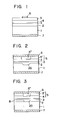
- Fig. 1 of the accompanying drawings which is a schematic sectional view showing principal parts of the laser.
- Fig. 2 of the accompanying drawings is a schematic sectional view showing principal parts of the laser, and in which parts corresponding to those in Fig. 1 are identified by the same reference numerals.
- the semiconductor laser of Fig. 2 differs from the semiconductor laser of Fig. 1 in that the clad layer 2 has a projecting portion 2G and in that the clad layer 2 outside of the projecting portion 2G is relatively thin.
- the cap layer 5 is composed of an n-type GaAs portion 5' and a p-type GaAs region 5'' for setting therein a current path.
- the semiconductor laser of Fig. 2 poses some problems in terms of its manufacture.
- the clad layer 2 is formed on substrate 1 in which a recess is made prior to the formation of the clad layer 2, and since the clad layer 2 is very thin except at its projecting portion 2G, there is a possibility that the clad layer 2 will sag at a position corresponding to the recess in the substrate 1 and consequently at a position corresponding to the projecting portion 2G, causing the active layer 3 to be curbed when formed. If the clad layer 2 is formed relatively thickly, to avoid this problem, then the light guide effect would be lost. Another problem is a difficulty in maintaining a desired shape for the recess formed in the substrate 1 for obtaining the projecting portion 2G.
- the desired edge shape of the recess 1G may be rounded of into the form of gentle slopes 1G'. The reason for this is as follows.
- the edge of the recess 1G is high in surface energy but other parts are low in surface energy, and when the growth solution makes contact with the substrate 1, the edge of the recess 1G is liable to be etched back by the solution.
- the light emitting region becomes wider as a current flows, making it impossible to maintain unity of the oscillation mode.
- Still anotherproblem is that it is very difficult to form the p-type GaAs region 5" for setting up a current path and the projecting portion 2G in alignment with each other.
- the amount of current which does not contribute to oscillation and which is therefore ineffective increases, with a resultant increase in a threshold current and an operating current, introducing non-uniformity into the light emission in the lateral direction and a change in the light emitting region.
- Fig. 3 of the accompanying drawings which is a schematic sectional view, illustrates principal parts of another previously proposed semiconductor laser which is different in construction from the semiconductor laser of Fig. 2.
- the former differs from the latter in that the n-type GaAs substrate 1 is formed flat, that-is, without having a recess therein; a p-type GaAs current preventing layer 8 is formed on the substrate 1; and after a groove is formed in the layer 8, the clad layer 2 is grown on the layer 8 to form the projecting portion 2G in the groove in layer 8.
- This semiconductor laser has the same defects as mentioned above in connection with Fig. 2 except in regard to current confinement.
- the p-type GaAs current preventing layer 8 considered to be advantageous over the semiconductor laser of Fig. 2 is of little or no use in practice.
- the p-type GaAs current preventing layer 8 absorb light of the active layer 3 leaking out of the clad layer 2. In the current preventing layer 8 electrons and holes are generated by absorbed light;the holes alone are gradually stored.
- the current preventing layer 8 is biased to a potential substantially equal to a diffusion potential between the substrate 1 and the clad layer 2.
- the current rejecting layer 8 is not sufficiently thick as compared with the diffusion length of minority carriers, electrons in the substrate 1 flow into the clad layer 2 through the current preventing layer 8, so that the current preventing layer 8 does not perform its function.
- the diffusion length of minority carriers depends on carrier concentration and it is 1 to 3 pm in the case of GaAs and, in order to ensure that the current preventing layer performs its function, the thickness of the layer must be 5 to 10 times the diffusion length of minority carriers. It is difficult to select the thickness of the current preventing layer 8 in the range up to 10 Am and to form the groove of 1 to 6 A m depth, for example, by means of etching. Moreover, it is difficult to select the distance between the active layer 3 and the current preventing layer 8 at a maximum as 0.4 ⁇ m and to form the active layer 3 flat. If the current preventing layer 8 and the active layer 3 are spaced apart by a distance of 1 ⁇ m or more, so as to prevent the current preventing layer 8 from absorbing light, the layer 8 always performs the current preventing function but the optical guide function is lost.
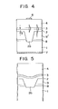
- a conventional semiconductor laser shown in Fig. 4 of the accompanying drawings which is a schematic sectional view, has also been proposed.
- Fig. 4 parts corresponding to those in Figs. 1 to 3 are identified by the same reference numerals.
- Fig. 4 8 is a p-type GaAlAs current preventing layer; and 9' is a p- or n-type GaAs layer.
- One of defects of this semiconductor laser is an increase in threshold current. That is, since use is made of what is called a loss guide system in which light is absorbed by the GaAs layer 9' on the outside of the stripe and is consequently guided in the stripe alone, the threshold current increases.
- Another defect is that the aetive layer 3 is formed with a hollow and cannot be made flat, as shown in Fig. 5 of the accompanying drawings, which is a schematic sectional view. The reason is that since the value 1 shown in Fig. 4 must be selected to be, for example, 0.3mm or less for guiding light, the active layer 3 is exposed directly to the influence of the groove.
- Still another defect is that since the GaAs layer 9' is thick, the gentle slope 1G' described previously in respect of Figs. 6 and 7 is produced as in the casesof the other previously proposed devices.
- an increase in the degree of supersaturation of the growth solution suppresses the etching-back of the edge of the recess during the formation of the clad layer but causes an increase in growth speed; accordingly, the clad layer tends to become thick, thereby to increase the distance between the active layer and the substrate, resulting in loss of optical guide function.
- the present invention can provide a semiconductor laser which is free from the abovementioned defects of previously proposed lasers which is equipped with a current confinement region setting function effective at all times, and an optical guide function unobtainable with the-previously proposed lasers and which is capable of stable oscillation in the lateral mode and which is easy to manufacture.
- Thepresent invention provides a semiconductor light emitting device in which a first growth layer of a low refractive index, a second growth layer of a high refractive index ultimately serving as an active layer and a third growth layer of a low refractive index are formed on a semiconductor compound substrate having formed therein a stripe-form hollow, and a current confining barrier is set up around the hollow, and which is characterized in that the first growth layer, an intermediate layer of a high refractive index, and a low refractive index layer are disposed on the surface of the substrate except within the hollow to establish a specified light oscillation mode cooperating with another light oscillation mode established by the active layerso that emissive light is essentially confined due to a difference in the effective refractive index between that part of the active layer overlying the hollow and other parts of the active layer.
- an etch-back preventive layer 9 is formed in addition to current preventing layer 8 and the forbidden band width of a predetermined layer is selected to be a certain value.
- the etch-back preventive layer 9 is an n-type GaAlAs layer and the amount of aluminium contained therein is held at a certain value, as described later.
- Fig. 9 shows refractive index and loss distributions in the stripe region defined by the projecting portion 2G and outside of the stripe region in the direction vertical to layer junctions in Fig. 8.
- Fig. 9(a) shows the distribution of the refractive indexes of the layers 2 to 4 in the stripe region
- Fig. 9(b) shows the distribution of the refractive indexes of the layers 2 to 4, and layers 8 and 9 outside the stripe region
- Fig. 9(c) shows the loss distributions.
- an even and an odd mode exist outside of the stripe region, as seen in Figs. 9(e) and (f), and light in the stripe region is coupled mainly with the odd mode.
- the propagation constant is made small as compared with that for the mode in the stripe region (see Fig. 9(d)) even if the thickness 1 of clad layer 2 is large.
- the effective refractive index outside of the stripe region is made smaller than the effective refractive index in the stripe region. As a consequence, light is confined to the stripe region.
- the refractive indexes of the respective layers were selected as follows:
- a refractive index difference necessary for controlling the lateral mode is required to be a relative effective refractive index difference of about 3x10- 3 .
- the solid-line curve A and the broken line curve B respectively indicate the effective refractive index and the loss in the device described previously in connection with Figs. 4 and 5.
- the effective refractive indexes inside and outside of the stripe region are substantially equal.
- the loss outside of the stripe region is as large as 800 cm -1 , which is in excess of 500 cm -1 which is an amountLloss necessary for guiding light.
- the thickness 1 of the clad layer 2 is in the range of 0.2 to 0.4 ⁇ m, the loss is smaller than 450 cm- 1 and no light is guided on the basis of the loss on the outside the stripe region.
- the effective refractive index on the outside of the stripe region is reduced to increase the effective refractive index difference between the inside and the outside of the stripe region, by which light is guided.
- the device described previously in connection with Figs. 4 and 5 utilizes the loss on the outside of the stripe region for guiding light, whereas in the present invention optical guiding is dependent on the effective refractive index difference between the inside and the outside of the stripe region.
- a change in the effective refractive index is large with respect to the thickness 1 of the clad layer 2, and in the case where the thickness h of the etch-back preventive layer 9 is 0.1 ⁇ m, even if the thickness 1 of the clad layer 2 is 0.5 ⁇ m, the odd mode provides a relative effective refractive index difference of 3x10 -3 . Accordingly, even if the thickness 1 of the clad layer 2 is large, effective confinement of light is possible.
- the thickness 1 of the clad layer 2 can be made large enables the active layer 3 to be formed flat, and hence is effective for enhancement of production yield in terms of crystal growth.
- the relationship between h and 1 necessary for obtaining the relative effective refractive index of 3x10 3 is such as shown in Fig. 11.
- the etch-back preventive layer 9 is provided, as shown in Fig. 8.
- the etch-back preventive layer 9 is a Ga 1-x Al x As layer, where 0.1>x>0.
- the GaAs substrate was subjected to the liquid phase epitaxial growth using each of the abovesaid solutions. Only in the case where the thickness h of the etch-back preventive layer 9 is selected to be smaller than 0.4 ⁇ m, evenif no aluminium is added, is the etch back is very slight; namely, the edge of the recess in the etch-back preventive layer 9 is rounded only slightly. Further, since the mixed crystal ratio of aluminium is large, the current preventing layer 8 is not etched back and does not substantially change its entire configuration.
- a p- type Ga 0.7 Al 0.3 As current preventing layer 8 is formed by the liquid phase epitaxy to a thickness of 0.5 to 1 ⁇ m on a silicon-doped GaAs substrate 1 which has a (100) plane and an electron concentration of 1x10 17 to 5 x10 18 . Then, an n-type Ga 0.99 Al 0.01 As etch-back preventive layer 9 is similarly formed to a thickness of 0.1 to 0.4 ⁇ m on the current preventing layer 8.
- a groove 2 to 10 ⁇ m wide is formed in the substrate assembly to extend down to the substrate 1.
- an n-type Ga 0.7 A 10.3 As clad layer 2 , a p- type Ga 0.95 Al 0.05 As active layer 3, a p-type Ga o.65 Al o . 35 A s clad layer 4 and a p-type GaAs cap layer 5 are formed by liquid phase epitaxy to thicknesses of 0.2 to 0.5 ⁇ m (in the portion of the layer 2 indicated by 1), 0.1 ⁇ m, 1 ⁇ m and 1 ⁇ m, respectively, on the substrate assembly.
- electrodes 6 and 7 are deposited by a known method on the cap layer 5 and the underside of the substrate 1, respectively. Then, the assembly is cleaved into individual chips about 300 ⁇ m long.
- the laser thus obtained exhibited a threshold current density of 1.2 KA/cm 2 at room temperature. Further, the laser oscillated stably in the lateral mode of the least order and no kink appeared in the current vs. optical output characteristic. Moreover, when the etch-back preventive layer 9 was formed thin, an excellent characteristic was obtained even if the thickness 1 of the clad layer 2 was about 0.5 ⁇ m.
- the thickness of the etch-back preventive layer 9 is selected to be 0.1 to 0.4 ⁇ m and the value x to be 0.01.
- the reason for selecting the thickness of the layer 9 in such a range is as follows: With a thickness less than 0.1 ⁇ m, the layer is too thin and difficult to form. Arid the thickness of the layer 9 with which it is possible to bbtain a relative effective refractive index difference of 3x10 -3 when the thickness I of the clad layer 2 is 0.2 ⁇ m, which is a feasible minimum value, is 0.4 ⁇ m. With a thickness exceeding this value, the abovesaid specific refractive index difference cannot be obtained and the lateral mode is unstable.
- the value x is not limited specifically to 0.01 mentioned in the above embodiment and can be selected in the range of 0.1 to 0. If the value x exceeds 0.1, an aluminium oxide film becomes rigid and the crystal to be grown thereon does not become excellent.
- the thickness of the clad layer 2 is selected to be 0.5 ⁇ m but this thickness can be selected in the range of 0.2 to 0.5 jAm. With 1 ⁇ 0.2 ⁇ m, the active layer 3 cannot be formed flat, and with 1>0.5 A m, even if the etch-back preventive layer.9 is formed to the feasible minimum thickness, i.e. 0.1 ⁇ m, it is impossible to obtain the relative effective refractive index difference 3x10 -3 which is necessary for stabilizing the lateral mode.
- Fig. 12 illustrates in section principal parts of another embodiment of the prevent invention
- parts corresponding to those in Fig. 8 are marked with the same reference numerals.
- This embodiment differs from the embodiment of Fig. 8 in that a cap layer 5' is an n-type GaAs layer, and in that zinc Zn is introduced in the cap layer 5' in a stripe pattern to form therein a p-type GaAs region.
- a slight misalignment of the p-type GaAs region 5" and the projecting portion 2G does not present such problems as were referred to previously with respect to the previously proposed devices shown in Figs. 2 and 3.
- the reason for this is that since the current preventing layer 8 in the present invention effectively performs its function at all times, the current path setting function is not required to be so strictly performed by the p-type GaAs region 5".
- the manufacture of the device of this embodiment is not so difficult, as compared with the abovementioned previously proposed devices.
- a threshold.current density of 1.1 KA/cm 2 was obtained and the lateral oscillation mode was also stable.
- the current preventing layer 8 was a p-type Ga 0.8 Al 0.2 As layer and the same characteristics as those of the embodiment of Fig. 8 were obtained.
- ternary compound semi-conductors are employed but of course, a quaternary compound can also be used.
- Fig. 13 illustrates an example of a semiconductor laser using a quaternary compound.
- 11 is an-n-type InP substrate (100 ⁇ m thick); 12 is an n-type IhP layer (1.5 ⁇ m thick); 13 is an n-tupe InGaAsP active layer (whose thickness is indicated by d); 14 is a p-type InP layer (whose thickness is indicated by 1); 15 is an n-type InGaAsP layer (whose thickness is indicated by h); 16 is an n-type InGaAsP (or InP) layer (1 ⁇ m thick); 17 is a p-type InP layer (1.5 ⁇ m thick); 18 is a p-type InGaAsP layer (1 ⁇ m thick); 19 is a Ti-tPt-Au electrode; 20 is an Au-Ge-Ni electrode; and S is the width of a stripe.
- the thicknesses d, 1 and h are 0.04 to 0.2, 0.2 to 0.5 and
- a current preventing layer and an etch-back preventive layer are provided in a semiconductor laser provided with a clad layer having a projecting portion for confining light from an active layer and a portion for oozing out the light or from which light leaks, and the forbidden band width and the conductivity type of each layer are specified.
- a semiconductor laser having an excellent current limit function and optical guide function, and in addition, the semiconductor laser is easy to manufacture.
Landscapes
- Physics & Mathematics (AREA)
- Geometry (AREA)
- Condensed Matter Physics & Semiconductors (AREA)
- General Physics & Mathematics (AREA)
- Electromagnetism (AREA)
- Optics & Photonics (AREA)
- Semiconductor Lasers (AREA)
- Liquid Deposition Of Substances Of Which Semiconductor Devices Are Composed (AREA)
Applications Claiming Priority (2)
| Application Number | Priority Date | Filing Date | Title |
|---|---|---|---|
| JP11632079A JPS5640292A (en) | 1979-09-11 | 1979-09-11 | Semiconductor laser |
| JP116320/79 | 1979-09-11 |
Publications (3)
| Publication Number | Publication Date |
|---|---|
| EP0025362A2 true EP0025362A2 (de) | 1981-03-18 |
| EP0025362A3 EP0025362A3 (en) | 1983-10-12 |
| EP0025362B1 EP0025362B1 (de) | 1987-04-01 |
Family
ID=14684059
Family Applications (1)
| Application Number | Title | Priority Date | Filing Date |
|---|---|---|---|
| EP80303169A Expired EP0025362B1 (de) | 1979-09-11 | 1980-09-10 | Licht emittierende Halbleitervorrichtung |
Country Status (5)
| Country | Link |
|---|---|
| US (1) | US4360919A (de) |
| EP (1) | EP0025362B1 (de) |
| JP (1) | JPS5640292A (de) |
| CA (1) | CA1167150A (de) |
| DE (1) | DE3071946D1 (de) |
Cited By (8)
| Publication number | Priority date | Publication date | Assignee | Title |
|---|---|---|---|---|
| WO1983003172A1 (en) * | 1982-03-04 | 1983-09-15 | Standard Telephones Cables Ltd | Injection laser manufacture |
| GB2145281A (en) * | 1983-08-18 | 1985-03-20 | Mitsubishi Electric Corp | Surface emitting semiconductor laser |
| DE3525703A1 (de) * | 1984-07-18 | 1986-02-20 | Sony Corp., Tokio/Tokyo | Halbleiterlaser |
| EP0106152A3 (en) * | 1982-09-13 | 1986-03-05 | Hitachi, Ltd. | Semiconductor laser device |
| EP0124051A3 (en) * | 1983-04-27 | 1987-04-08 | Kabushiki Kaisha Toshiba | Semiconductor laser |
| EP0156365A3 (en) * | 1984-03-28 | 1987-06-03 | Kabushiki Kaisha Toshiba | Semiconductor laser |
| EP0452869A1 (de) * | 1990-04-16 | 1991-10-23 | Canon Kabushiki Kaisha | Verfahren zur Herstellung einer Halbleiter-Vorrichtung |
| DE4330987A1 (de) * | 1992-09-14 | 1994-03-31 | Sharp Kk | Halbleiterlaser |
Families Citing this family (17)
| Publication number | Priority date | Publication date | Assignee | Title |
|---|---|---|---|---|
| US4511408A (en) * | 1982-04-22 | 1985-04-16 | The Board Of Trustees Of The University Of Illinois | Semiconductor device fabrication with disordering elements introduced into active region |
| GB2105099B (en) * | 1981-07-02 | 1985-06-12 | Standard Telephones Cables Ltd | Injection laser |
| JPS5967677A (ja) * | 1982-07-01 | 1984-04-17 | Semiconductor Res Found | 光集積回路 |
| JPS5990979A (ja) * | 1982-11-16 | 1984-05-25 | Nec Corp | 半導体レ−ザ |
| GB2139422B (en) * | 1983-03-24 | 1987-06-03 | Hitachi Ltd | Semiconductor laser and method of fabricating the same |
| US4631729A (en) * | 1983-12-01 | 1986-12-23 | Trw Inc. | Semiconductor laser structure |
| US4633477A (en) * | 1984-07-20 | 1986-12-30 | Trw Inc. | Semiconductor laser with blocking layer |
| JPS60192380A (ja) * | 1984-03-13 | 1985-09-30 | Mitsubishi Electric Corp | 半導体レ−ザ装置 |
| JPS60206081A (ja) * | 1984-03-29 | 1985-10-17 | Sharp Corp | 半導体レ−ザ装置 |
| US5136601A (en) * | 1984-11-19 | 1992-08-04 | Hitachi, Ltd. | Semiconductor laser |
| US4647320A (en) * | 1985-05-22 | 1987-03-03 | Trw Inc. | Method of making a surface emitting light emitting diode |
| US4694311A (en) * | 1985-05-22 | 1987-09-15 | Trw Inc. | Planar light-emitting diode |
| JPH07118559B2 (ja) * | 1985-06-18 | 1995-12-18 | 松下電器産業株式会社 | 半導体レ−ザ装置 |
| US4783425A (en) * | 1985-11-06 | 1988-11-08 | Hitachi, Ltd. | Fabrication process of semiconductor lasers |
| US4788159A (en) * | 1986-09-18 | 1988-11-29 | Eastman Kodak Company | Process for forming a positive index waveguide |
| JPS63138232A (ja) * | 1986-11-29 | 1988-06-10 | Tokyo Electron Ltd | 振動試験システム |
| US5443450A (en) * | 1994-04-29 | 1995-08-22 | Medtronic, Inc. | Medication delivery device and method of construction |
Family Cites Families (3)
| Publication number | Priority date | Publication date | Assignee | Title |
|---|---|---|---|---|
| US4326176A (en) * | 1976-04-16 | 1982-04-20 | Hitachi, Ltd. | Semiconductor laser device |
| JPS5451491A (en) * | 1977-09-30 | 1979-04-23 | Hitachi Ltd | Semiconductor laser |
| DE3065856D1 (en) * | 1979-02-13 | 1984-01-19 | Fujitsu Ltd | A semiconductor light emitting device |
-
1979
- 1979-09-11 JP JP11632079A patent/JPS5640292A/ja active Granted
-
1980
- 1980-09-10 DE DE8080303169T patent/DE3071946D1/de not_active Expired
- 1980-09-10 EP EP80303169A patent/EP0025362B1/de not_active Expired
- 1980-09-10 US US06/185,806 patent/US4360919A/en not_active Expired - Lifetime
- 1980-09-11 CA CA000360120A patent/CA1167150A/en not_active Expired
Cited By (10)
| Publication number | Priority date | Publication date | Assignee | Title |
|---|---|---|---|---|
| WO1983003172A1 (en) * | 1982-03-04 | 1983-09-15 | Standard Telephones Cables Ltd | Injection laser manufacture |
| EP0106152A3 (en) * | 1982-09-13 | 1986-03-05 | Hitachi, Ltd. | Semiconductor laser device |
| EP0124051A3 (en) * | 1983-04-27 | 1987-04-08 | Kabushiki Kaisha Toshiba | Semiconductor laser |
| GB2145281A (en) * | 1983-08-18 | 1985-03-20 | Mitsubishi Electric Corp | Surface emitting semiconductor laser |
| US4675875A (en) * | 1983-08-18 | 1987-06-23 | Mitsubishi Denki Kabushiki Kaisha | Surface emitting semiconductor laser |
| EP0156365A3 (en) * | 1984-03-28 | 1987-06-03 | Kabushiki Kaisha Toshiba | Semiconductor laser |
| DE3525703A1 (de) * | 1984-07-18 | 1986-02-20 | Sony Corp., Tokio/Tokyo | Halbleiterlaser |
| EP0452869A1 (de) * | 1990-04-16 | 1991-10-23 | Canon Kabushiki Kaisha | Verfahren zur Herstellung einer Halbleiter-Vorrichtung |
| DE4330987A1 (de) * | 1992-09-14 | 1994-03-31 | Sharp Kk | Halbleiterlaser |
| DE4330987B4 (de) * | 1992-09-14 | 2007-05-16 | Sharp Kk | Halbleiterlaser mit Strom- und Lichteingrenzstruktur |
Also Published As
| Publication number | Publication date |
|---|---|
| DE3071946D1 (en) | 1987-05-07 |
| JPS5640292A (en) | 1981-04-16 |
| EP0025362B1 (de) | 1987-04-01 |
| CA1167150A (en) | 1984-05-08 |
| US4360919A (en) | 1982-11-23 |
| EP0025362A3 (en) | 1983-10-12 |
| JPS5722428B2 (de) | 1982-05-13 |
Similar Documents
| Publication | Publication Date | Title |
|---|---|---|
| EP0025362A2 (de) | Licht emittierende Halbleitervorrichtung | |
| US4635268A (en) | Semiconductor laser device having a double heterojunction structure | |
| US4033796A (en) | Method of making buried-heterostructure diode injection laser | |
| US4328469A (en) | High output power injection lasers | |
| US4371966A (en) | Heterostructure lasers with combination active strip and passive waveguide strip | |
| US4425650A (en) | Buried heterostructure laser diode | |
| EP0535307B1 (de) | Halbleiterlaser | |
| EP0155152A2 (de) | Halbleiterlaser | |
| US4321556A (en) | Semiconductor laser | |
| EP0000412A2 (de) | Halbleiter-Injektionslaser oder-verstärker | |
| EP1416598B1 (de) | Lichtemittierendes Halbleiterbauelement in dem eine starke Ausgangslichtleistung durch eine einfache Struktur erziehlt wird | |
| EP0264225B1 (de) | Halbleiterlaservorrichtung und Verfahren zur Herstellung derselben | |
| KR900003844B1 (ko) | 반도체 레이저장치와 그 제조방법 | |
| US4429397A (en) | Buried heterostructure laser diode | |
| US4977568A (en) | Semiconductor laser device | |
| US5770471A (en) | Method of making semiconductor laser with aluminum-free etch stopping layer | |
| US4464211A (en) | Method for selective area growth by liquid phase epitaxy | |
| JPH0815229B2 (ja) | 埋め込み型半導体レ−ザ | |
| US4983541A (en) | Semiconductor laser device fabrication | |
| US4866723A (en) | DCPBH laser having a high temperature stability | |
| CA1173550A (en) | Semiconductor light emitting device | |
| JP2909144B2 (ja) | 半導体レーザ装置及びその製造方法 | |
| US4392227A (en) | Terraced substrate semiconductor laser | |
| JP2988552B2 (ja) | 半導体レーザ装置及びその製造方法 | |
| JPS6237557B2 (de) |
Legal Events
| Date | Code | Title | Description |
|---|---|---|---|
| PUAI | Public reference made under article 153(3) epc to a published international application that has entered the european phase |
Free format text: ORIGINAL CODE: 0009012 |
|
| AK | Designated contracting states |
Designated state(s): DE FR GB NL |
|
| RBV | Designated contracting states (corrected) |
Designated state(s): DE FR GB NL |
|
| 17P | Request for examination filed |
Effective date: 19811029 |
|
| PUAL | Search report despatched |
Free format text: ORIGINAL CODE: 0009013 |
|
| RHK1 | Main classification (correction) |
Ipc: H01S 3/19 |
|
| AK | Designated contracting states |
Designated state(s): DE FR GB NL |
|
| GRAA | (expected) grant |
Free format text: ORIGINAL CODE: 0009210 |
|
| AK | Designated contracting states |
Kind code of ref document: B1 Designated state(s): DE FR GB |
|
| ET | Fr: translation filed | ||
| REF | Corresponds to: |
Ref document number: 3071946 Country of ref document: DE Date of ref document: 19870507 |
|
| PLBE | No opposition filed within time limit |
Free format text: ORIGINAL CODE: 0009261 |
|
| STAA | Information on the status of an ep patent application or granted ep patent |
Free format text: STATUS: NO OPPOSITION FILED WITHIN TIME LIMIT |
|
| 26N | No opposition filed | ||
| PGFP | Annual fee paid to national office [announced via postgrant information from national office to epo] |
Ref country code: GB Payment date: 19920707 Year of fee payment: 13 |
|
| PGFP | Annual fee paid to national office [announced via postgrant information from national office to epo] |
Ref country code: DE Payment date: 19921125 Year of fee payment: 13 |
|
| PG25 | Lapsed in a contracting state [announced via postgrant information from national office to epo] |
Ref country code: GB Effective date: 19930910 |
|
| GBPC | Gb: european patent ceased through non-payment of renewal fee |
Effective date: 19930910 |
|
| PG25 | Lapsed in a contracting state [announced via postgrant information from national office to epo] |
Ref country code: DE Effective date: 19940601 |
|
| PGFP | Annual fee paid to national office [announced via postgrant information from national office to epo] |
Ref country code: FR Payment date: 19950911 Year of fee payment: 16 |
|
| PG25 | Lapsed in a contracting state [announced via postgrant information from national office to epo] |
Ref country code: FR Effective date: 19960930 |
|
| REG | Reference to a national code |
Ref country code: FR Ref legal event code: ST |
|
| REG | Reference to a national code |
Ref country code: FR Ref legal event code: ST |