EP0452919B1 - Circuit intégré semi-conducteur Bi-MOS - Google Patents
Circuit intégré semi-conducteur Bi-MOS Download PDFInfo
- Publication number
- EP0452919B1 EP0452919B1 EP91106210A EP91106210A EP0452919B1 EP 0452919 B1 EP0452919 B1 EP 0452919B1 EP 91106210 A EP91106210 A EP 91106210A EP 91106210 A EP91106210 A EP 91106210A EP 0452919 B1 EP0452919 B1 EP 0452919B1
- Authority
- EP
- European Patent Office
- Prior art keywords
- bipolar transistor
- power supply
- base
- output terminal
- source
- Prior art date
- Legal status (The legal status is an assumption and is not a legal conclusion. Google has not performed a legal analysis and makes no representation as to the accuracy of the status listed.)
- Expired - Lifetime
Links
- 239000004065 semiconductor Substances 0.000 title claims description 21
- 230000000694 effects Effects 0.000 description 7
- 239000000758 substrate Substances 0.000 description 6
- 238000010586 diagram Methods 0.000 description 4
- 230000003071 parasitic effect Effects 0.000 description 4
- 230000007423 decrease Effects 0.000 description 2
- 238000007599 discharging Methods 0.000 description 2
- 238000000034 method Methods 0.000 description 1
- 230000000116 mitigating effect Effects 0.000 description 1
- 230000007704 transition Effects 0.000 description 1
Images
Classifications
-
- H—ELECTRICITY
- H03—ELECTRONIC CIRCUITRY
- H03K—PULSE TECHNIQUE
- H03K19/00—Logic circuits, i.e. having at least two inputs acting on one output; Inverting circuits
- H03K19/02—Logic circuits, i.e. having at least two inputs acting on one output; Inverting circuits using specified components
- H03K19/08—Logic circuits, i.e. having at least two inputs acting on one output; Inverting circuits using specified components using semiconductor devices
- H03K19/094—Logic circuits, i.e. having at least two inputs acting on one output; Inverting circuits using specified components using semiconductor devices using field-effect transistors
- H03K19/0944—Logic circuits, i.e. having at least two inputs acting on one output; Inverting circuits using specified components using semiconductor devices using field-effect transistors using MOSFET or insulated gate field-effect transistors, i.e. IGFET
- H03K19/0948—Logic circuits, i.e. having at least two inputs acting on one output; Inverting circuits using specified components using semiconductor devices using field-effect transistors using MOSFET or insulated gate field-effect transistors, i.e. IGFET using CMOS or complementary insulated gate field-effect transistors
-
- H—ELECTRICITY
- H03—ELECTRONIC CIRCUITRY
- H03K—PULSE TECHNIQUE
- H03K19/00—Logic circuits, i.e. having at least two inputs acting on one output; Inverting circuits
- H03K19/02—Logic circuits, i.e. having at least two inputs acting on one output; Inverting circuits using specified components
- H03K19/08—Logic circuits, i.e. having at least two inputs acting on one output; Inverting circuits using specified components using semiconductor devices
- H03K19/094—Logic circuits, i.e. having at least two inputs acting on one output; Inverting circuits using specified components using semiconductor devices using field-effect transistors
- H03K19/0944—Logic circuits, i.e. having at least two inputs acting on one output; Inverting circuits using specified components using semiconductor devices using field-effect transistors using MOSFET or insulated gate field-effect transistors, i.e. IGFET
- H03K19/09448—Logic circuits, i.e. having at least two inputs acting on one output; Inverting circuits using specified components using semiconductor devices using field-effect transistors using MOSFET or insulated gate field-effect transistors, i.e. IGFET in combination with bipolar transistors [BIMOS]
-
- H—ELECTRICITY
- H03—ELECTRONIC CIRCUITRY
- H03K—PULSE TECHNIQUE
- H03K19/00—Logic circuits, i.e. having at least two inputs acting on one output; Inverting circuits
- H03K19/01—Modifications for accelerating switching
- H03K19/013—Modifications for accelerating switching in bipolar transistor circuits
Definitions
- the present invention relates to a Bi-MOS semiconductor integrated circuit in which a bipolar transistor is formed at an output stage, according to the preamble of the claims 1 and 5.
- An integrated circuit of this kind is known from EP-A-0 099 100.
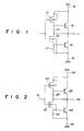
- Fig. 1 shows the structure of part of a conventional Bi-CMOS semiconductor integrated circuit in which a signal is processed by a logic circuit comprising P-and N-channel MOSFETs and a bipolar transistor is formed at an output stage to enhance the current driving force against an output load.
- a logic circuit comprising P-and N-channel MOSFETs and a bipolar transistor is formed at an output stage to enhance the current driving force against an output load.
- reference numeral 11 denotes a signal output terminal
- 12 shows a P-channel MOS FET for charging the output terminal 11 to be set at a high potential
- 13 indicates an NPN bipolar transistor, formed at the output stage, for charging the output terminal 11 to be set at a high potential
- 14 represents a resistor for emitting surplus base charges from the bipolar transistor 13 to increase the speed at which the on-state of the bipolar transistor 13 changes to the off-state thereof
- 15 indicates an N-channel MOS FET for discharging the output terminal 11 to be set at a low potential
- 16 shows an NPN bipolar transistor, formed at the output stage, for discharging the output terminal to be set at a low potential
- 17 denotes a resistor for emitting surplus base charges from the bipolar transistor 16 to increase the speed at which the on-state of the bipolar transistor 16 changes to the off-state thereof
- 18 indicates a power supply terminal to which a high power supply voltage V cc is applied
- 19 represents a power supply terminal to which a
- the back gate of the N-channel MOSFET 15 is connected to the power supply terminal 19 for the reason that an N-channel MOSFET is usually formed on the surface region of a P-type semiconductor substrate and the lowest voltage, that is, a low power supply voltage V ss is applied to the semiconductor substrate.
- the source potential of the N-channel MOSFET 15 does not always correspond to the back gate potential thereof. If the back gate potential becomes lower than the source potential, the mutual inductance gm of the MOSFET is reduced by the well-known back gate bias effect.
- the mutual inductance is reduced by the back gate bias effect particularly in a transition from the off-state of the MOSFET 15 to the on-state thereof. More specifically, if the MOSFET 15 is turned on, a base current flows into the bipolar transistor 16 through the MOSFET 15 and the bipolar transistor 16 is thus turned on. When the bipolar transistor 16 starts to be turned on, a voltage drop is caused in the parasitic base resistance of the transistor 16 and thus the source potential of the MOSFET 15 becomes higher than the power supply voltage V ss . Since the back gate of the MOSFET 15 is always connected to the power supply terminal 19, the back gate potential of the MOSFET 15 is made lower than the source potential thereof by the voltage drop. The difference between the source potential and the back gate potential is considerably larger than a voltage (about 0.7 V) between the base and emitter of a common bipolar transistor. For example, the source potential of the MOSFET 15 increases up to about 2 V.
- Bi-MOS semiconductor integrated circuit in which the falling speed of an output signal can be increased by mitigating the back gate bias effect of a MOSFET for driving the base of a bipolar transistor formed at an output stage.
- a Bi-MOS semiconductor integrated circuit comprising:
- N first nodes for receiving N input signals (N is a positive integer, N being greater than 1; an output terminal for outputting a signal; a first power supply terminal for receiving a first power supply voltage; a second power supply terminal for receiving a second power supply voltage; an NPN type first bipolar transistor having a collector connected to said output terminal, an emitter connected to said first power supply terminal, and a base; N N-channel MOSFETs each having a gate, a drain, a source, and a back gate, said gate being connected to a corresponding one of said N first nodes, drain-to-source paths of said N-channel MOSFETs being connected in series between said output terminal and the base of said first bipolar transistor; an NPN type second bipolar transistor having a collector connected to said second power supply terminal, an emitter connected to said output terminal, and a base; and N P-channel MOSFETs each having a gate, a drain, and a source, said gate being connected to a corresponding one of said N first nodes, source-to-
- Fig. 2 illustrates the structure of part of a Bi-CMOS semiconductor integrated circuit.
- a node 21 is supplied with an input signal.
- the gates of P- and N-channel MOSFETs 22 and 23 are connected to the node 21.
- the source and back gate of the MOSFET 22 are connected to a power supply terminal 24 to which a high power supply voltage V CC is applied.
- the drain of the MOSFET 22 is connected to the base of an NPN bipolar transistor 25.
- the collector of the bipolar transistor 25 is connected to the power supply terminal 24 and the emitter thereof is connected to an output terminal 26 for outputting a signal.
- a resistor 27 is inserted between the base of the bipolar transistor 25 and the output terminal 26, to serve as a means for supplying surplus charges from the base to the output terminal 26 when the bipolar transistor 25 changes from the on-state to the off-state.
- the drain of the N-channel MOSFET 23 is connected to the output terminal 26.
- the source and back gate of the MOSFET 23 are connected in common to the base of an NPN bipolar transistor 28.
- the collector of the bipolar transistor 28 is connected to the output terminal 26, the emitter thereof is connected to a power supply terminal 29 to which a power supply voltage V SS of ground potential is applied.
- a resistor 30 is inserted between the base of the bipolar transistor 28 and the power supply terminal 29, to serve as a means for supplying surplus charges from the base to the power supply terminal 29 when the bipolar transistor 28 changes from the on-state to the off-state.
- the signal at the node 21 is then changed from low level to high level.
- the conductive P-channel MOSFET 22 and bipolar transistor 25 are turned off, and the N-channel MOSFET 23 is turned on. Electric charges are emitted from the output terminal 26 whose signal level is high to the power supply terminal 29 through the MOSFET 23 and resistor 30. Further, since the base current is supplied through the MOSFET 23, the bipolar transistor 28 is turned on and the output terminal 26 is discharged.
- the MOSFET 23 and bipolar transistor 28 are rendered conductive, the surplus charges are emitted from the base of the bipolar transistor 25 and the speed at which the transistor 25 changes from the on-state to the off-state is increased.
- the back gate of an N-channel MOSFET is usually formed on the surface region of a P-type semiconductor substrate and a low power supply voltage V ss is always applied to the semiconductor substrate. If the N-channel MOSFET is formed on the P-type semiconductor substrate as it is, its back gate and source cannot be connected to each other.
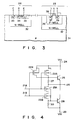
- Fig. 3 is a cross-sectional view showing the structure of part of the circuit shown in Fig. 2. As shown in Fig. 3, a plurality of N-well regions 32 is formed on a P-type semiconductor substrate 31 to attain the circuit shown in Fig. 2. An NPN bipolar transistor, which is to be provided at the output stage, is formed in one of the N-well regions 32. Fig. 3 illustrates the bipolar transistor 28 including a collector contact region 33, a base region 34 and an emitter region 35.
- a plurality of P well regions 36 is formed in one of the N-well regions 32 (only one P-well region is shown in Fig. 3) and an N-channel MOSFET is formed in each of the P-well regions 36.
- Fig. 3 illustrates the MOSFET 23 including a drain region 37, a gate electrode 38 and a source region 39. Since the P-well regions 36 are formed independently of one another, each of them can be formed in contact with the source region 39.
- N positive integer
- the circuit of the embodiment differs from that of the figure 2 in that two nodes 21A and 21B supplied with an input signal are arranged in place of the node 21, two P-channel MOSFETs 22A and 22B are arranged in place of the P-channel MOSFET 22, and two N-channel MOSFETs 23A and 23B are arranged in place of the N-channel MOSFET 23.
- the source-to-drain paths of the two P-channel MOSFETs 22A and 22B are connected in parallel between the V cc power supply terminal 24 and the base of the bipolar transistor 25 and the gates of the MOSFETs 22A and 22B are connected to the nodes 21A and 21B, respectively.
- the source-to-drain paths of the N-channel MOSFETs 23A and 23B are connected in series between the output terminal 26 and the base of the bipolar transistor 28 and the gates of the MOSFETs 23A and 23B are connected to the nodes 21A and 21B, respectively.
- the back gates of the N-channel MOSFETs 23A and 23B are connected to the source of the MOSFET 23B, the source being directly connected to the base of the bipolar transistor 28.
- the back gate of the MOSFET 23A can be connected to the source of the MOSFET 23A instead of being connected to the source of the MOSFET 23B.
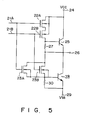
- the circuit according to figure 5 differs from that of the embodiment in the methods of connecting the two P-channel MOSFETs 22A and 22B and connecting the two N-channel MOSFETs 23A and 23B.
- the source-to-drain paths of the P-channel MOSFETs 22A and 22B are connected in series between the V CC power supply terminal 24 and the base of the bipolar transistor 25.
- the source-to-drain paths of the N-channel MOSFETs 23A and 23B are connected in parallel between the output terminal 26 and the base of the bipolar transistor 28.
Landscapes
- Engineering & Computer Science (AREA)
- Physics & Mathematics (AREA)
- Computer Hardware Design (AREA)
- Computing Systems (AREA)
- General Engineering & Computer Science (AREA)
- Mathematical Physics (AREA)
- Power Engineering (AREA)
- Logic Circuits (AREA)
- Metal-Oxide And Bipolar Metal-Oxide Semiconductor Integrated Circuits (AREA)
- Electronic Switches (AREA)
Claims (4)
- Circuit intégré semiconducteur Bi-CMOS comportant :N premiers noeuds (21A, 21B) pour recevoir N signaux d'entrée (N est un entier positif) supérieur à 1;une borne de sortie (26) pour délivrer un signal;une première borne d'alimentation (29) pour recevoir une première tension d'alimentation (VSS);une seconde borne d'alimentation (24) pour recevoir une seconde tension d'alimentation (VCC);un premier transistor bipolaire de type NPN (28) ayant un collecteur relié à ladite borne de sortie, un émetteur relié à ladite première borne d'alimentation, et une base;N transistors MOS à canal N (23A, 23B) ayant chacun une grille, un drain, une source et une grille auxiliaire, ladite grille étant reliée à l'un correspondant desdits N premiers modes, des trajets drain-source desdits transistors MOS à canal N étant reliés en série entre ladite borne de sortie et la base dudit premier transistor bipolaire;un second transistor bipolaire de type NPN (25) ayant un collecteur relié à ladite seconde borne d'alimentation, un émetteur relié à ladite borne de sortie, et une base; etN transistors MOS à canal P (22A, 22B), chacun possédant une grille, un drain, et une source, ladite grille étant reliée à l'un correspondant desdits N premiers noeuds, les trajets source-drain desdits transistors MOS à canal P étant reliés en parallèle entre la seconde borne d'alimentation et la base dudit second transistor bipolaire;caractérisé en ce que
ladite grille auxiliaire de chacun desdits N transistors MOS à canal N (23A, 23B) est reliée à ladite source qui est reliée à la base dudit premier transistor bipolaire (28). - Circuit intégré semiconducteur Bi-CMOS selon la revendication 1, caractérisé en ce qu'une tension de masse (VSS) est appliquée à ladite première borne d'alimentation (29) en tant que première tension d'alimentation, et une tension élevée (VCC) est appliquée à ladite seconde borne d'alimentation (24) en tant que seconde tension d'alimentation.
- Circuit intégré semiconducteur Bi-CMOS selon la revendication 1, caractérisé en ce que les grilles auxiliaires desdits N transistors MOS à canal N (23A, 23B) sont réunies à la base dudit premier transistor bipolaire.
- Circuit intégré semiconducteur Bi-CMOS selon la revendication 1, caractérisé en ce qu'il comporte en outre :des premiers moyens (30), introduits entre la base dudit premier transistor bipolaire et ladite première borne d'alimentation, afin d'extraire des charges excédentaires de la base dudit premier transistor bipolaire; etdes seconds moyens (27), introduits entre la base dudit second transistor bipolaire et ladite borne de sortie, pour extraire des charges excédentaires de la base dudit second transistor bipolaire.
Applications Claiming Priority (2)
| Application Number | Priority Date | Filing Date | Title |
|---|---|---|---|
| JP2104579A JPH043619A (ja) | 1990-04-20 | 1990-04-20 | 半導体集積回路 |
| JP104579/90 | 1990-04-20 |
Publications (3)
| Publication Number | Publication Date |
|---|---|
| EP0452919A2 EP0452919A2 (fr) | 1991-10-23 |
| EP0452919A3 EP0452919A3 (en) | 1991-11-13 |
| EP0452919B1 true EP0452919B1 (fr) | 1996-11-20 |
Family
ID=14384348
Family Applications (1)
| Application Number | Title | Priority Date | Filing Date |
|---|---|---|---|
| EP91106210A Expired - Lifetime EP0452919B1 (fr) | 1990-04-20 | 1991-04-18 | Circuit intégré semi-conducteur Bi-MOS |
Country Status (5)
| Country | Link |
|---|---|
| US (1) | US5126595A (fr) |
| EP (1) | EP0452919B1 (fr) |
| JP (1) | JPH043619A (fr) |
| KR (1) | KR940007299B1 (fr) |
| DE (1) | DE69123167T2 (fr) |
Families Citing this family (8)
| Publication number | Priority date | Publication date | Assignee | Title |
|---|---|---|---|---|
| US5430408A (en) * | 1993-03-08 | 1995-07-04 | Texas Instruments Incorporated | Transmission gate circuit |
| USRE38398E1 (en) | 1996-02-14 | 2004-01-27 | L'oreal S.A. | Case for a cosmetic care product with a flexible bottom |
| FR2744602B1 (fr) * | 1996-02-14 | 1998-03-06 | Oreal | Boitier notamment de maquillage et/ou de soin a fond souple |
| US6025676A (en) * | 1996-03-06 | 2000-02-15 | Kabushiki Kaisha Toshiba | Cathode ray tube having improved curvature characteristics and method of fabrication thereof |
| JP3485092B2 (ja) * | 2001-01-19 | 2004-01-13 | セイコーエプソン株式会社 | 半導体装置およびその製造方法 |
| JP2006061189A (ja) * | 2004-08-24 | 2006-03-09 | Key Tranding Co Ltd | 化粧料容器 |
| CN103490766A (zh) * | 2013-08-29 | 2014-01-01 | 苏州苏尔达信息科技有限公司 | 一种高速高精度源极跟随电路 |
| KR101805162B1 (ko) * | 2017-04-17 | 2017-12-05 | 충남대학교산학협력단 | 수분 저항성 및 내구성이 우수한 유기성 고밀도 제재 및 이의 제조방법 |
Citations (1)
| Publication number | Priority date | Publication date | Assignee | Title |
|---|---|---|---|---|
| EP0305098A2 (fr) * | 1987-08-25 | 1989-03-01 | AT&T Corp. | Tampon de sortie pour la conversion de signaux CMOS en signaux ECL |
Family Cites Families (9)
| Publication number | Priority date | Publication date | Assignee | Title |
|---|---|---|---|---|
| JPH0783252B2 (ja) * | 1982-07-12 | 1995-09-06 | 株式会社日立製作所 | 半導体集積回路装置 |
| KR910008521B1 (ko) * | 1983-01-31 | 1991-10-18 | 가부시기가이샤 히다찌세이사꾸쇼 | 반도체집적회로 |
| JPS60125015A (ja) * | 1983-12-12 | 1985-07-04 | Hitachi Ltd | インバ−タ回路 |
| JPH07107973B2 (ja) * | 1984-03-26 | 1995-11-15 | 株式会社日立製作所 | スイツチング回路 |
| US4703203A (en) * | 1986-10-03 | 1987-10-27 | Motorola, Inc. | BICMOS logic having three state output |
| JPS6468021A (en) * | 1987-09-08 | 1989-03-14 | Mitsubishi Electric Corp | Logic circuit |
| JP2696991B2 (ja) * | 1988-09-26 | 1998-01-14 | 日本電気株式会社 | BiCMOS論理回路 |
| JPH03136365A (ja) * | 1989-10-23 | 1991-06-11 | Oki Electric Ind Co Ltd | バイポーラmis複合半導体装置 |
| JPH03280713A (ja) * | 1990-03-29 | 1991-12-11 | Nec Corp | BiCMOS論理ゲート回路 |
-
1990
- 1990-04-20 JP JP2104579A patent/JPH043619A/ja active Pending
-
1991
- 1991-04-18 EP EP91106210A patent/EP0452919B1/fr not_active Expired - Lifetime
- 1991-04-18 DE DE69123167T patent/DE69123167T2/de not_active Expired - Fee Related
- 1991-04-19 US US07/689,707 patent/US5126595A/en not_active Expired - Lifetime
- 1991-04-20 KR KR1019910006352A patent/KR940007299B1/ko not_active Expired - Fee Related
Patent Citations (1)
| Publication number | Priority date | Publication date | Assignee | Title |
|---|---|---|---|---|
| EP0305098A2 (fr) * | 1987-08-25 | 1989-03-01 | AT&T Corp. | Tampon de sortie pour la conversion de signaux CMOS en signaux ECL |
Non-Patent Citations (1)
| Title |
|---|
| DeWitt G. Ong, "Modern MOS Technology: Processes, Devices and Design", McGraw-Hill Book Company, 1984, pages 90-95 * |
Also Published As
| Publication number | Publication date |
|---|---|
| US5126595A (en) | 1992-06-30 |
| DE69123167T2 (de) | 1997-04-10 |
| KR940007299B1 (ko) | 1994-08-12 |
| DE69123167D1 (de) | 1997-01-02 |
| KR910019340A (ko) | 1991-11-30 |
| EP0452919A3 (en) | 1991-11-13 |
| EP0452919A2 (fr) | 1991-10-23 |
| JPH043619A (ja) | 1992-01-08 |
Similar Documents
| Publication | Publication Date | Title |
|---|---|---|
| EP0145004B1 (fr) | Circuit composite, transistors bipolaires-transistors à effet de champ | |
| KR920004919B1 (ko) | 반도체 집적회로 장치 | |
| KR100207338B1 (ko) | 드라이버 회로 | |
| US5376816A (en) | Bi-cmos integrated circuit device having buried region use in common for bipolar and mos transistors | |
| US4694202A (en) | Bi-MOS buffer circuit | |
| EP0243603B1 (fr) | Circuit logique binaire | |
| US4952825A (en) | Semiconductor integrated circuit having signal level conversion circuit | |
| EP0250947A2 (fr) | Porte logique Bimos | |
| US5079447A (en) | BiCMOS gates with improved driver stages | |
| EP0307323B1 (fr) | Inverseur à transistor bipolaire et transistors MOS complémentaires | |
| EP0452919B1 (fr) | Circuit intégré semi-conducteur Bi-MOS | |
| US5663678A (en) | ESD protection device | |
| US4890018A (en) | Bipolar-complementary metal oxide semiconductor circuit | |
| KR100264497B1 (ko) | 구동기 회로 | |
| US4806797A (en) | bi-CMOS buffer cascaded to CMOS driver having PMOS pull-up transistor with threshold voltage greater than VBE of bi-CMOS bipolar pull-up transistor | |
| US4977337A (en) | Bi-CMOS logic circuit | |
| US5168341A (en) | Bipolar-cmos integrated circuit having a structure suitable for high integration | |
| EP0439894B1 (fr) | Circuit logique à semi-conducteur | |
| US5124582A (en) | Bi-cmos circuit with high-speed active pull-down output currents | |
| US5164617A (en) | High speed bicmos logic circuit | |
| JP2978346B2 (ja) | 半導体集積回路装置の入力回路 | |
| JP2714996B2 (ja) | 半導体集積回路装置 | |
| EP0225489A2 (fr) | Circuit logique | |
| US5428302A (en) | Logic circuit with controlled current supply output | |
| JP2694808B2 (ja) | ソリッドステートリレー |
Legal Events
| Date | Code | Title | Description |
|---|---|---|---|
| PUAI | Public reference made under article 153(3) epc to a published international application that has entered the european phase |
Free format text: ORIGINAL CODE: 0009012 |
|
| PUAL | Search report despatched |
Free format text: ORIGINAL CODE: 0009013 |
|
| 17P | Request for examination filed |
Effective date: 19910418 |
|
| AK | Designated contracting states |
Kind code of ref document: A2 Designated state(s): DE FR GB |
|
| AK | Designated contracting states |
Kind code of ref document: A3 Designated state(s): DE FR GB |
|
| 17Q | First examination report despatched |
Effective date: 19941215 |
|
| GRAG | Despatch of communication of intention to grant |
Free format text: ORIGINAL CODE: EPIDOS AGRA |
|
| GRAH | Despatch of communication of intention to grant a patent |
Free format text: ORIGINAL CODE: EPIDOS IGRA |
|
| RAP1 | Party data changed (applicant data changed or rights of an application transferred) |
Owner name: KABUSHIKI KAISHA TOSHIBA |
|
| GRAH | Despatch of communication of intention to grant a patent |
Free format text: ORIGINAL CODE: EPIDOS IGRA |
|
| GRAA | (expected) grant |
Free format text: ORIGINAL CODE: 0009210 |
|
| AK | Designated contracting states |
Kind code of ref document: B1 Designated state(s): DE FR GB |
|
| REF | Corresponds to: |
Ref document number: 69123167 Country of ref document: DE Date of ref document: 19970102 |
|
| ET | Fr: translation filed | ||
| PGFP | Annual fee paid to national office [announced via postgrant information from national office to epo] |
Ref country code: FR Payment date: 19970409 Year of fee payment: 7 |
|
| PGFP | Annual fee paid to national office [announced via postgrant information from national office to epo] |
Ref country code: DE Payment date: 19970428 Year of fee payment: 7 |
|
| PLBE | No opposition filed within time limit |
Free format text: ORIGINAL CODE: 0009261 |
|
| STAA | Information on the status of an ep patent application or granted ep patent |
Free format text: STATUS: NO OPPOSITION FILED WITHIN TIME LIMIT |
|
| 26N | No opposition filed | ||
| PG25 | Lapsed in a contracting state [announced via postgrant information from national office to epo] |
Ref country code: FR Free format text: THE PATENT HAS BEEN ANNULLED BY A DECISION OF A NATIONAL AUTHORITY Effective date: 19980430 |
|
| REG | Reference to a national code |
Ref country code: GB Ref legal event code: 746 Effective date: 19981010 |
|
| PG25 | Lapsed in a contracting state [announced via postgrant information from national office to epo] |
Ref country code: DE Free format text: LAPSE BECAUSE OF NON-PAYMENT OF DUE FEES Effective date: 19990202 |
|
| REG | Reference to a national code |
Ref country code: FR Ref legal event code: ST |
|
| REG | Reference to a national code |
Ref country code: GB Ref legal event code: IF02 |
|
| PGFP | Annual fee paid to national office [announced via postgrant information from national office to epo] |
Ref country code: GB Payment date: 20100325 Year of fee payment: 20 |
|
| REG | Reference to a national code |
Ref country code: GB Ref legal event code: PE20 Expiry date: 20110417 |
|
| PG25 | Lapsed in a contracting state [announced via postgrant information from national office to epo] |
Ref country code: GB Free format text: LAPSE BECAUSE OF EXPIRATION OF PROTECTION Effective date: 20110417 |