EP0452976B1 - RF modulator requiring no test pattern generator - Google Patents
RF modulator requiring no test pattern generator Download PDFInfo
- Publication number
- EP0452976B1 EP0452976B1 EP91106443A EP91106443A EP0452976B1 EP 0452976 B1 EP0452976 B1 EP 0452976B1 EP 91106443 A EP91106443 A EP 91106443A EP 91106443 A EP91106443 A EP 91106443A EP 0452976 B1 EP0452976 B1 EP 0452976B1
- Authority
- EP
- European Patent Office
- Prior art keywords
- signal
- channel
- channel setting
- modulator
- video signal
- Prior art date
- Legal status (The legal status is an assumption and is not a legal conclusion. Google has not performed a legal analysis and makes no representation as to the accuracy of the status listed.)
- Expired - Lifetime
Links
- 208000019300 CLIPPERS Diseases 0.000 claims description 20
- 208000021930 chronic lymphocytic inflammation with pontine perivascular enhancement responsive to steroids Diseases 0.000 claims description 20
- 230000005236 sound signal Effects 0.000 claims description 10
- 230000010355 oscillation Effects 0.000 claims 4
- 239000003990 capacitor Substances 0.000 description 6
- 238000010586 diagram Methods 0.000 description 6
- 238000010276 construction Methods 0.000 description 1
- 238000000034 method Methods 0.000 description 1
Images


Classifications
-
- H—ELECTRICITY
- H04—ELECTRIC COMMUNICATION TECHNIQUE
- H04N—PICTORIAL COMMUNICATION, e.g. TELEVISION
- H04N5/00—Details of television systems
- H04N5/76—Television signal recording
- H04N5/78—Television signal recording using magnetic recording
- H04N5/782—Television signal recording using magnetic recording on tape
-
- G—PHYSICS
- G11—INFORMATION STORAGE
- G11B—INFORMATION STORAGE BASED ON RELATIVE MOVEMENT BETWEEN RECORD CARRIER AND TRANSDUCER
- G11B33/00—Constructional parts, details or accessories not provided for in the other groups of this subclass
-
- H—ELECTRICITY
- H04—ELECTRIC COMMUNICATION TECHNIQUE
- H04N—PICTORIAL COMMUNICATION, e.g. TELEVISION
- H04N5/00—Details of television systems
- H04N5/44—Receiver circuitry for the reception of television signals according to analogue transmission standards
- H04N5/50—Tuning indicators; Automatic tuning control
Definitions
- This invention relates to an RF modulator, and more particularly to an RF modulator built in the VCR (video cassette recorder) which performs TV channel setting by the frequency synthesizer technique.
- VCR video cassette recorder
- the VCR video cassette recorder
- the VCR generally incorporates an RF modulator that RF (radio frequency)-converts the signal from the signal processing system to produce a signal suitable for TV (television).
- the video signal is amplitude-modulated by the amplitude modulator at the frequency generated at the RF carrier oscillator.
- the audio signal is frequency-modulated by the frequency modulator at the frequency generated at the audio carrier oscillator.
- the frequency-modulated audio signal is further converted, by the frequency converter, into the frequency generated at the RF carrier oscillator.
- the amplitude-modulated video signal and the once-frequency-converted audio signal are added to form an RF signal output, which is in turn transmitted to the TV system.
- Channel setting for a playback of videotape is made by changing the oscillating frequency of the RF carrier oscillator at its variable capacitor.
- the purpose of channel setting is to put video and audio signals in a vacant TV channel.
- Each country requires its unique channel setting in the UHF band. To deal with this situation, the variable capacitor is used to cover a wide channel setting range.
- the user operates the channel setting mode switch to activate the test pattern generator, whose output signal is connected to the video signal system, with the result that the generatorcreated test pattern is converted into an RF signal that is supplied to the TV system.
- the TV has received a vacant channel previously.
- the variable capacitor is adjusted so that the test pattern appears on the vacant channel.
- the test pattern generator is disconnected to switch to the normal mode.
- variable capacitor is used to change the oscillating frequency of the RF carrier oscillator for TV channel setting.
- Recent VCRs produce signals usable in place of the test pattern for channel setting, such as a signal that makes the entire screen blue or what is called a blue back. This makes it unnecessary to operate the test pattern generator to supply the test pattern.
- US-A-4,500,920 shows an RF modulator with a carrier generator circuit for both audio and video, and means for combining modulated video and audio signals.
- A/D converter or a channel picking-up means or signal cut-off means.
- the object of the present invention is to provide an RF modulator without a test pattern generator which enables stable TV reception by channel setting.
- the present invention provides an RF modulator as set out in claim 1.
- the channel picking-up means picks up a portion near the center of each channel in the A/D converter-digitized channel setting data, while the clipper circuit substantially cuts off the video signal at a suitable clipping level at both ends of each channel setting range that have not been picked up. This makes the channel setting immune to temperature drift and change with passage of time in terms of mechanical accuracy.
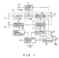
- Fig. 1 is a block diagram showing the structure of an RF modulator according to a first embodiment of the present invention.
- a varactor diode-based voltage-controlled oscillator is used in place of a variable capacitor difficult to use for stable TV reception.
- the oscillator is connected into the PLL (phase-locked loop) to compose a frequency synthesizer-type RF modulator that digitally controls the control voltage of the varactor diode.
- the video signal S1 supplied to terminal 11 is amplitude-modulated, by a modulator unit 12, at the frequency generated by an RF carrier oscillator 13.
- the modulator unit 12 is composed of a clamper circuit 14, a clipper circuit 15, and an amplitude modulator 16.
- the clipper circuit 15 is controlled by a clipper control circuit 17.
- the audio signal S2 supplied to terminal 18 is frequency-modulated, by a frequency modulator 19, at the frequency produced at the audio carrier oscillator 20.
- This frequency-modulated audio signal S2 is then converted into an RF frequency by frequency converter 21 which also receives the frequency generated by the RF carrier oscillator 13.
- the amplitude-modulated video signal S1 and the once-frequency-modulated frequency-converted audio signal S2 are added together at an adder 22 and the result appears as the RF signal S out at terminal 23.
- Both the RF carrier oscillator 13 and the audio carrier oscillator 20 are controlled by an oscillator control circuit 24.
- the analog input signal from a variable resistor VR serving as an external adjusting element is converted into a digital signal at an A/D converter 25. This digital signal is supplied to both the oscillator control circuit 24 and clipper control circuit 17.
- the oscillator control circuit 24 determines the frequency dividing ratio and the channel setting data for changing its output frequencies on the basis of the digital signal from the A/D converter 25.
- the RF carrier oscillator 13 compares its own frequency with that of the oscillator control circuit 24 at a tuning varactor diode 26, which is comprised in a PLL. In this way, the oscillating frequency for each of the audio carrier oscillator 20 and RF carrier oscillator 13 is set digitally.
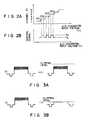
- the A/D converter 25 supplies individual channel setting data, in the form of the input voltage of a specific value from the external adjusting element VR and with a specific range of values, to the clipper control circuit 17. Then, the clipper control circuit 17 outputs a control signal that functions in such a way that the channel setting may not be made at both ends of each channel voltage range set at the A/D converter, these ends adjoining the preceding and succeeding ranges. That is, as shown in Fig. 2B, with the clipper control circuit 17, when the setting voltage is present near the center of the channel setting range, the signal V H is supplied, but otherwise, the signal V L is supplied.
- the clipper circuit 15 changes the clipping level as shown in Figs. 3A and 3B.
- the circuit 15 performs the normal white clipping of video signal S1 to prevent overmodulation, whereas for the input of signal V L , it substantially cuts off the video signal S1 with the clipping level at a low value.
- VCR signal system supplies a video signal distinguishable from other stations's broadcasts, such as a blue back.
- the TV reception channel is set for a vacant channel not occupied by a TV station.
- the channel setting mode switch 27 (shown in Fig. 1) of the RF modulator is then turned on.
- the variable resistor VR is adjusted so that the video signal from the VCR signal system such as a blue back may appear on the screen.
- the RF modulator's channel setting switch 27 is then turned off.
- Fig. 4 is a block diagram showing the structure of an RF modulator according to a second embodiment of the present invention.
- the arrangement of Fig. 4 is the same as that of Fig. 1 except that a switch 28 is connected between the clamper circuit 14 and the clipper circuit 15 and a switch control circuit 29 is provided in place of the clipper control circuit 17 to control the switch 28.
- the switch control circuit 29 produces the signal V H when the setting voltage is near the center of the channel setting range, but otherwise it generates the signal V L .
- the channel setting range for each channel is supplied in the form of the input voltage from the A/D converter 25.
- the switch control circuit 29 turns the switch 28 on during the existence of signal V H , causing the clipper circuit 15 to carry out the normal white clipping of video signal S1 to prevent overmodulation. During the period of signal V L , it turns the switch 28 off to cut off the video signal S1.
- a frequency/amplitude modulator 30 capable of both frequency and amplitude modulations may be used instead of the frequency modulator 19.
- Fig. 5 shows an application of the frequency/amplitude modulator to the Fig. 1's arrangement. The same holds true for the Fig. 4's arrangement.
Landscapes
- Engineering & Computer Science (AREA)
- Multimedia (AREA)
- Signal Processing (AREA)
- Transmitters (AREA)
- Testing, Inspecting, Measuring Of Stereoscopic Televisions And Televisions (AREA)
Applications Claiming Priority (2)
| Application Number | Priority Date | Filing Date | Title |
|---|---|---|---|
| JP2107151A JP2553219B2 (ja) | 1990-04-23 | 1990-04-23 | Rfモジュレータ及びそれを内蔵するビデオカセットレコーダ |
| JP107151/90 | 1990-04-23 |
Publications (3)
| Publication Number | Publication Date |
|---|---|
| EP0452976A2 EP0452976A2 (en) | 1991-10-23 |
| EP0452976A3 EP0452976A3 (en) | 1993-02-10 |
| EP0452976B1 true EP0452976B1 (en) | 1996-06-19 |
Family
ID=14451803
Family Applications (1)
| Application Number | Title | Priority Date | Filing Date |
|---|---|---|---|
| EP91106443A Expired - Lifetime EP0452976B1 (en) | 1990-04-23 | 1991-04-22 | RF modulator requiring no test pattern generator |
Country Status (5)
| Country | Link |
|---|---|
| US (1) | US5136387A (ko) |
| EP (1) | EP0452976B1 (ko) |
| JP (1) | JP2553219B2 (ko) |
| KR (1) | KR930011597B1 (ko) |
| DE (1) | DE69120335T2 (ko) |
Families Citing this family (3)
| Publication number | Priority date | Publication date | Assignee | Title |
|---|---|---|---|---|
| US5369445A (en) * | 1992-06-12 | 1994-11-29 | Samsung Electronics Co., Ltd. | Noise reducing apparatus and methods for television receivers |
| US6118497A (en) * | 1998-03-11 | 2000-09-12 | Thomson Consumer Electronics, Inc. | Interactive selection system for a video decoder modulator channel |
| KR100550875B1 (ko) * | 2004-02-27 | 2006-02-10 | 삼성전기주식회사 | 협대역 밴드패스 필터를 포함하는 고주파 모듈레이터 |
Family Cites Families (6)
| Publication number | Priority date | Publication date | Assignee | Title |
|---|---|---|---|---|
| US3778718A (en) * | 1972-04-28 | 1973-12-11 | Avco Corp | Modulation system |
| FR2437117A1 (fr) * | 1978-09-22 | 1980-04-18 | Lgt Lab Gen Telecomm | Systeme de transmission en modulation d'amplitude a haute performance et emetteur et reemetteur de television comportant un tel systeme |
| US4286336A (en) * | 1979-02-08 | 1981-08-25 | Rca Corporation | Automatic shutdown arrangement for stand-alone television modulator |
| JPS583672U (ja) * | 1981-07-01 | 1983-01-11 | アルプス電気株式会社 | Rf変調装置 |
| US4491871A (en) * | 1982-12-06 | 1985-01-01 | Rca Corporation | Audio-visual diplexed television transmitter in which the aural signal can be multiplexed without switching |
| JPS60220683A (ja) * | 1984-04-17 | 1985-11-05 | Murata Mfg Co Ltd | Vtrのrfモジユレ−タ |
-
1990
- 1990-04-23 JP JP2107151A patent/JP2553219B2/ja not_active Expired - Fee Related
-
1991
- 1991-04-22 EP EP91106443A patent/EP0452976B1/en not_active Expired - Lifetime
- 1991-04-22 US US07/688,313 patent/US5136387A/en not_active Expired - Lifetime
- 1991-04-22 DE DE69120335T patent/DE69120335T2/de not_active Expired - Fee Related
- 1991-04-23 KR KR1019910006486A patent/KR930011597B1/ko not_active Expired - Fee Related
Also Published As
| Publication number | Publication date |
|---|---|
| EP0452976A3 (en) | 1993-02-10 |
| US5136387A (en) | 1992-08-04 |
| DE69120335T2 (de) | 1996-12-12 |
| KR910019045A (ko) | 1991-11-30 |
| DE69120335D1 (de) | 1996-07-25 |
| KR930011597B1 (ko) | 1993-12-13 |
| JPH0418876A (ja) | 1992-01-23 |
| EP0452976A2 (en) | 1991-10-23 |
| JP2553219B2 (ja) | 1996-11-13 |
Similar Documents
| Publication | Publication Date | Title |
|---|---|---|
| KR100196250B1 (ko) | Rf변조기 | |
| CA1125444A (en) | Tuning apparatus | |
| JPS627728B2 (ko) | ||
| US5029237A (en) | Radio receiver frequency control system | |
| EP0456099B1 (en) | On channel agile FM demodulator | |
| KR960000523B1 (ko) | 수신기 | |
| EP0452976B1 (en) | RF modulator requiring no test pattern generator | |
| US5995169A (en) | SIF signal processing circuit | |
| EP0735715A3 (en) | Radio communication terminal station | |
| CA1149978A (en) | Search type tuning system | |
| GB2056800A (en) | Aft arrangement for a phase locked loop tuning system | |
| JPS5924191Y2 (ja) | シンセサイザ−受信機のafc回路 | |
| US4941050A (en) | An afc arrangement for tuning a television receiving apparatus to a select transmission having an actual carrier frequency which differs from a nominal carrrier frequency | |
| JPS6132852B2 (ko) | ||
| JPS593616Y2 (ja) | 掃引形選局装置 | |
| JP2880223B2 (ja) | テレビジョン受信機 | |
| JPH03270507A (ja) | Afc回路 | |
| JPS6234177B2 (ko) | ||
| JP2611268B2 (ja) | ディジタル音声放送受信装置 | |
| JPH0787412A (ja) | 放送信号受信装置 | |
| JP2790121B2 (ja) | 受信機 | |
| JPH0846549A (ja) | 周波数ホッピングスペクトル拡散通信方式の送受信機 | |
| KR970004909Y1 (ko) | 브이씨알의 알에프(rf)출력 티브이(tv)수신장치 | |
| JPH03173226A (ja) | 選局同調回路 | |
| JPH08316738A (ja) | Rfモジュレータ |
Legal Events
| Date | Code | Title | Description |
|---|---|---|---|
| PUAI | Public reference made under article 153(3) epc to a published international application that has entered the european phase |
Free format text: ORIGINAL CODE: 0009012 |
|
| 17P | Request for examination filed |
Effective date: 19910422 |
|
| AK | Designated contracting states |
Kind code of ref document: A2 Designated state(s): DE FR GB IT |
|
| PUAL | Search report despatched |
Free format text: ORIGINAL CODE: 0009013 |
|
| AK | Designated contracting states |
Kind code of ref document: A3 Designated state(s): DE FR GB IT |
|
| RAP1 | Party data changed (applicant data changed or rights of an application transferred) |
Owner name: TOSHIBA AVE CO., LTD Owner name: KABUSHIKI KAISHA TOSHIBA |
|
| 17Q | First examination report despatched |
Effective date: 19950207 |
|
| GRAH | Despatch of communication of intention to grant a patent |
Free format text: ORIGINAL CODE: EPIDOS IGRA |
|
| GRAA | (expected) grant |
Free format text: ORIGINAL CODE: 0009210 |
|
| AK | Designated contracting states |
Kind code of ref document: B1 Designated state(s): DE FR GB IT |
|
| ITF | It: translation for a ep patent filed | ||
| REF | Corresponds to: |
Ref document number: 69120335 Country of ref document: DE Date of ref document: 19960725 |
|
| GRAH | Despatch of communication of intention to grant a patent |
Free format text: ORIGINAL CODE: EPIDOS IGRA |
|
| ET | Fr: translation filed | ||
| PGFP | Annual fee paid to national office [announced via postgrant information from national office to epo] |
Ref country code: FR Payment date: 19970409 Year of fee payment: 7 |
|
| PGFP | Annual fee paid to national office [announced via postgrant information from national office to epo] |
Ref country code: GB Payment date: 19970414 Year of fee payment: 7 |
|
| PLBE | No opposition filed within time limit |
Free format text: ORIGINAL CODE: 0009261 |
|
| STAA | Information on the status of an ep patent application or granted ep patent |
Free format text: STATUS: NO OPPOSITION FILED WITHIN TIME LIMIT |
|
| PGFP | Annual fee paid to national office [announced via postgrant information from national office to epo] |
Ref country code: DE Payment date: 19970428 Year of fee payment: 7 |
|
| 26N | No opposition filed | ||
| PG25 | Lapsed in a contracting state [announced via postgrant information from national office to epo] |
Ref country code: GB Free format text: LAPSE BECAUSE OF NON-PAYMENT OF DUE FEES Effective date: 19980422 |
|
| PG25 | Lapsed in a contracting state [announced via postgrant information from national office to epo] |
Ref country code: FR Free format text: THE PATENT HAS BEEN ANNULLED BY A DECISION OF A NATIONAL AUTHORITY Effective date: 19980430 |
|
| GBPC | Gb: european patent ceased through non-payment of renewal fee |
Effective date: 19980422 |
|
| PG25 | Lapsed in a contracting state [announced via postgrant information from national office to epo] |
Ref country code: DE Free format text: LAPSE BECAUSE OF NON-PAYMENT OF DUE FEES Effective date: 19990202 |
|
| REG | Reference to a national code |
Ref country code: FR Ref legal event code: ST |
|
| PGFP | Annual fee paid to national office [announced via postgrant information from national office to epo] |
Ref country code: IT Payment date: 20060430 Year of fee payment: 16 |
|
| PG25 | Lapsed in a contracting state [announced via postgrant information from national office to epo] |
Ref country code: IT Free format text: LAPSE BECAUSE OF NON-PAYMENT OF DUE FEES Effective date: 20070422 |