EP0453110B1 - Synchronisation von digitalen Audiosignalen - Google Patents
Synchronisation von digitalen Audiosignalen Download PDFInfo
- Publication number
- EP0453110B1 EP0453110B1 EP91302723A EP91302723A EP0453110B1 EP 0453110 B1 EP0453110 B1 EP 0453110B1 EP 91302723 A EP91302723 A EP 91302723A EP 91302723 A EP91302723 A EP 91302723A EP 0453110 B1 EP0453110 B1 EP 0453110B1
- Authority
- EP
- European Patent Office
- Prior art keywords
- timing
- input
- pulses
- delay
- write
- Prior art date
- Legal status (The legal status is an assumption and is not a legal conclusion. Google has not performed a legal analysis and makes no representation as to the accuracy of the status listed.)
- Expired - Lifetime
Links
Images

Classifications
-
- G—PHYSICS
- G06—COMPUTING OR CALCULATING; COUNTING
- G06F—ELECTRIC DIGITAL DATA PROCESSING
- G06F5/00—Methods or arrangements for data conversion without changing the order or content of the data handled
- G06F5/06—Methods or arrangements for data conversion without changing the order or content of the data handled for changing the speed of data flow, i.e. speed regularising or timing, e.g. delay lines, FIFO buffers; over- or underrun control therefor
- G06F5/10—Methods or arrangements for data conversion without changing the order or content of the data handled for changing the speed of data flow, i.e. speed regularising or timing, e.g. delay lines, FIFO buffers; over- or underrun control therefor having a sequence of storage locations each being individually accessible for both enqueue and dequeue operations, e.g. using random access memory
- G06F5/12—Means for monitoring the fill level; Means for resolving contention, i.e. conflicts between simultaneous enqueue and dequeue operations
-
- H—ELECTRICITY
- H03—ELECTRONIC CIRCUITRY
- H03K—PULSE TECHNIQUE
- H03K5/00—Manipulating of pulses not covered by one of the other main groups of this subclass
- H03K5/13—Arrangements having a single output and transforming input signals into pulses delivered at desired time intervals
- H03K5/135—Arrangements having a single output and transforming input signals into pulses delivered at desired time intervals by the use of time reference signals, e.g. clock signals
-
- G—PHYSICS
- G06—COMPUTING OR CALCULATING; COUNTING
- G06F—ELECTRIC DIGITAL DATA PROCESSING
- G06F2205/00—Indexing scheme relating to group G06F5/00; Methods or arrangements for data conversion without changing the order or content of the data handled
- G06F2205/12—Indexing scheme relating to groups G06F5/12 - G06F5/14
- G06F2205/123—Contention resolution, i.e. resolving conflicts between simultaneous read and write operations
Definitions
- This invention relates to the reception and synchronisation of digital signals, and particularly digital audio signals.
- FIFO first in, first out stores
- Constraints are placed on the relative timing of the read and write operations for these stores.
- Such a store has a "busy" output line which is enabled whenever either a write operation or a read operation takes place which inhibits any simultaneous attempt at a read or write operation respectively.
- US-A-4054747 discloses a system which compares read and write timing signals. If a read/write violation occurs, in which two or more read signals occur between successive write signals, or two or more write signals occur between successive read signals, the violation is detected and the write and read signal timings are adjusted accordingly.
- GB-A-2030740 discloses a circuit in which read/write violations are prevented by delaying the write signals to prevent collision.
- the system disclosed is prone to multiple data skips and repeats if the phasing between read and write pulses is such that the latch circuit holding a count changes back and forth between 7 and 8.
- the delay applied to data samples then changes between 14 and 0 giving multiple data skips and repeats. This is not a problem in the video signal environment to which it is applied but makes it unsuitable for sample-by-sample correction.
- a preferred digital signal receiving and synchronising system embodying the invention and designed particularly for use with audio signals is described in more detail below with reference to the drawings.
- a digital audio signal which is subject to sample-to-sample jitter is synchronised with local reference pulses by the use of a read-write buffer memory.
- Timing pulses are associated with the input samples.
- the input samples are applied through a one-sample latch store to the main memory, and the timing pulses are applied by switches either directly or a short delay to the write control input of the main memory.
- a phase comparator detects sample-by-sample when the write pulses are near to the read pulses and causes the switches to change state in response thereto, and they retain their changed state until a danger of potential read-write contention is again detected when they revert to their original state.
- FIG. 2 is a block schematic of one embodiment of the invention.
- the circuit 10 illustrated includes a FIFO store 12 which can contain three input samples and provides a buffer function for the audio samples received at an input 14.
- the audio signals are received in conjunction with a WRITE timing signal at a terminal 80.
- the memory 12 provides output samples to an output 16 in response to READ pulses received at a terminal 18 and applied to a read control circuit 74.
- the output samples may then be applied to a digital to analogue converter for example.
- the converter requires audio sample data consistently synchronous with the READ pulses.
- the write pulses at input 80 are associated with audio samples received at the input 14, and in this case both are derived from the same source, though the write pulses may be produced in other ways. In normal operation, these pulses are used as a latching signal applied to the latching input 82 of an added memory 36, and a short time ⁇ t1 later after passing through a delay element 62, as write pulses for the main memory 12. ⁇ t1 is a very short delay equal to the propagation delay of the added memory 36.
- the output of the added memory 36 is connected directly to the input of the main memory by line 22. Thus, in normal operation, the added memory behaves virtually transparently, adding a small propagation delay to the input of the main memory.
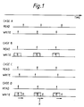
- a phase comparator 24 compares the write and read pulses applied to the main memory. If a write pulse approaches too closely to a read pulse, the phase comparator provides a single pulse at its output. This pulse is applied by control line 50 to switches 66,68. These switches allow a relatively long delay element 38 of delay ⁇ t2 to be admitted into the write signal path. Thus, dependent upon the positions of linked switches 66,68 the write pulses arrive at the write control circuit 72 of the main memory either directly through line 70, or through the delay 38 of value ⁇ t2. The magnitude ⁇ t2 of the delay 38 is greater than the overall expected peak-to-peak timing jitter as shown by the shaded area in Figure 1 at B.
- the added memory 36 contains one location, and therefore requires only a latch signal 82. The output of this additional memory on line 22 is equal to the latched contents after a short propagation delay.
- the system checks read and write signal pulses for every incoming audio sample, and is thus able to follow sample-by-sample timing variations of the type found in digital audio systems (as opposed to slowly drifting variation relative to a fixed reference). Each measurement relates to an individual sample.
- Switches 66,68 change state each time a pulse is received from the phase comparator i.e. they operate as toggles. That is, once the delay 38 has been brought into use, further measurements are made using the thus-delayed WRITE pulses, until potential read/write contention is again detected. Then the delay 38 is no longer used.
- Such an arrangement makes for a much more elegant design and only requires a few memory locations.
- the maximum allowable jitter can be defined for a given level of communication link performance.
- the phase or timing difference is measured by reference to a high frequency clock, that is a clock which has a frequency much higher than the data rate. This measurement itself introduces an additional jitter component which must also be allowed for in the calculation of delay value ⁇ t2. If the measured phase difference is greater than the peak jitter possible, then data passes transparently through the additional memory 36 subject to a small delay ⁇ t1. If the measured phase difference is smaller than the maximum jitter possible, then the data is held in the additional memory for a much longer time ⁇ t2. After this time it is written to main memory.
- the additional memory 36 and the main memory 12 can be constituted by a single 4-sample memory with the additional memory 36 being constituted by the first sample location of the memory.
- Figure 3 illustrates a possible circuit for use as the phase comparator 24 to detect instances of potential read/write contention.
- Read pulses are received at terminal 18 and write pulses at a terminal 40.
- the read pulses are applied through two delays 42,44 of the same length as delay 38.
- a gate 46 is opened by the read pulses received at terminal 18 and is closed by the pulses from the output of delay 44.
- the write pulses are applied to a similar delay 48 and thence to the gate 46. If a delayed write pulse arrives at the gate when it is open, then the pulse passes through the gate and toggles the switches 66,68.
- the circuits illustrated can be implemented in the form of an integrated circuit device and can be incorporated into a digital audio interface in accordance with IEC 958. They have the advantage of providing synchronism in a system where the master clock is not derived from the input pulses and yet provide a very small overall delay to the signal.
Landscapes
- Physics & Mathematics (AREA)
- Engineering & Computer Science (AREA)
- Theoretical Computer Science (AREA)
- Nonlinear Science (AREA)
- General Engineering & Computer Science (AREA)
- General Physics & Mathematics (AREA)
- Synchronisation In Digital Transmission Systems (AREA)
- Signal Processing For Digital Recording And Reproducing (AREA)
- Communication Control (AREA)
- Stereo-Broadcasting Methods (AREA)
- Television Signal Processing For Recording (AREA)
Claims (9)
- Verfahren zum Empfangen eines digitalen Signals, dessen Abtastwerte (Samples) einer zeitlichen Unsicherheit unterliegen, und zu ihrer Synchronisation mit einer Referenzquelle, enthaltend die Schritte:
Vorsehen eines Haupt-Lese-Schreib-Speichers (12), der in der Lage ist, wenigstens einen Eingangsdatenabtastwert zu speichern, und der einen Dateneingang, einen Datenausgang, einen Schreibsteuereingang und einen Lesesteuereingang hat;
selektiv in einer von zwei möglichen Betriebsarten erfolgendes Anlegen der Eingangsabtastwerte und auch von Zeitsteuerimpulsen, die auf die Eingangsabtastwerte bezogen sind, an den Hauptspeicher, und zwar entweder in einer ersten Betriebsart durch Anlegen der Zeitsteuerimpulse an den Schreibsteuereingang des Hauptspeichers und Anlegen der Eingangsdatenabtastwerte an den Dateneingang des Hauptspeichers im wesentlichen ohne Verzögerung in bezug auf die Schreibzeitsteuerimpulse oder in einer zweiten Betriebsart durch Anlegen der Zeitsteuerimpulse an den Schreibsteuereingang über eine Zeitsteuerimpulsverzögerung (38) und Anlegen der Eingangsabtastwerte an den Dateneingang über eine Datenabtastwertverzögerung (36); und
Vergleichen der Zeitabfolge aufeinanderfolgender Impulse, die dem Schreibsteuereingang und dem Lesesteuereingang des Hauptspeichers zugeführt werden, und, falls sich die Impulse bis auf weniger als einen vorbestimmten auf die zeitliche Unsicherheit des Eingangssignals bezogenen Zeitabstand nähern, Ändern der Betriebsart des Anlegens der Zeitsteuerimpulse und der Eingangsabtastwerte an den Hauptspeicher, wobei der Zeitabfolgevergleich nach der Verzögerung der Zeitsteuerimpulse in der zweiten Betriebsart ausgeführt wird. - Verfahren nach Anspruch 1, bei dem das digitale Signal ein digitales Audiosignal ist.
- Digitalsignalempfangs- und Synchronisiervorrichtung zum Empfangen eines digitalen Signals, dessen Abtastwerte (Samples) einer zeitlichen Unsicherheit unterliegen, und zu ihrer Synchronisation mit einer Referenzquelle, enthaltend:
einen Signaleingang (14) zum Empfangen des digitalen Signals;
eine Einrichtung zum Vorsehen von Zeitsteuerimpulsen entsprechend dem Empfang von Abtastwerten beim Signaleingang;
einen Anschluß (18) zum Empfangen von Referenzimpulsen, in bezug auf die das digitale Signal zu synchronisieren ist;
eine Haupt-Lese-Schreib-Speichereinrichtung (12), die in der Lage ist, wenigstens einen Abtastwert zu speichern, und die einen Dateneingang, einen den Ausgang der Vorrichtung bildenden Datenausgang, einen Schreibsteuereingang und einen Lesesteuereingang hat, der mit dem Anschluß zum Empfangen von Referenzimpulsen verbunden ist;
eine zusätzliche Speichereinrichtung (36), die zum Speichern eines Abtastwertes fähig ist;
eine Zeitsteuerimpulsverzögerung (38);
eine einen Steuereingang aufweisende Selektoreinrichtung (66, 68), die in einem ersten Zustand Impulse von der Zeitsteuerimpulse vorsehenden Einrichtung an die Schreibsteuereinrichtung der Hauptspeichereinrichtung legt und den Signaleingang an den Dateneingang der Hauptspeichereinrichtung im wesentlichen ohne Verzögerung in der zusätzlichen Speichereinrichtung in bezug auf die Zeitsteuerimpulse von der Zeitsteuerimpulse vorsehenden Einrichtung legt und die in einem zweiten Zustand die Zeitsteuerimpulse vorsehende Einrichtung über die Zeitsteuerimpulsverzögerung mit der Schreibsteuereinrichtung der Hauptspeichereinrichtung verbindet und den Signaleingang über die zusätzliche Speichereinrichtung mit dem Dateneingang der Hauptspeichereinrichtung verbindet; und
eine Zeitabfolgevergleichseinrichtung (24), die so verbunden ist, daß sie aufeinanderfolgende Impulse empfängt, die dem Schreibsteuereingang und dem Lesesteuereingang der Hauptspeichereinrichtung zugeführt werden, um deren Zeitabfolge zu vergleichen und, falls sich die Impulse bis auf weniger als einen vorbestimmten auf die zeitliche Unsicherheit des Eingabesignals bezogenen Zeitabstand nähern, ein Steuersignal an den Steuereingang der Selektoreinrichtung zu legen und dadurch deren Zustand von ihrem ersten Zustand zu ihrem zweiten Zustand, oder umgekehrt, wie es der Fall sein mag, zu ändern, wobei die Zeitabfolgevergleichseinrichtung derart verbunden wird, daß sie aufeinanderfolgende Impulse nach Verzögerung durch die Zeitsteuerimpulsverzögerung in dem zweiten Zustand empfängt. - Vorrichtung nach Anspruch 3, bei der die Zeitsteuerimpulsverzögerung wenigstens gleich dem vorbestimmten Zeitabstand ist.
- Vorrichtung nach Anspruch 3 oder 4, bei der in dem ersten Zustand der Selektoreinrichtung die zusätzliche Speichereinrichtung für das Eingangssignal wirksam durchlässig gemacht ist.
- Vorrichtung nach irgendeinem der Ansprüche 3 bis 5, bei der die Hauptspeichereinrichtung zum Speichern von drei Abtastwerten fähig ist.
- Vorrichtung nach irgendeinem der Ansprüche 3 bis 6, bei der die Hauptspeichereinrichtung und die zusätzliche Speichereinrichtung durch einen einzigen Speicher gebildet sind.
- Vorrichtung nach irgendeinem der Ansprüche 3 bis 7, bei der die Zeitabfolgevergleichseinrichtung eine erste Zeitabfolgevergleichsverzögerung (42, 44) zum Verzögern von an dem Anschluß empfangenen Referenzimpulsen um einen Betrag enthält, der im wesentlichen das Zweifache der Verzögerung der Zeitsteuerimpulsverzögerung ist, eine zweite Zeitabfolgevergleichsverzögerung (48) zum Verzögern der dem Schreibsteuereingang der Hauptspeichereinrichtung zugeführten Impulse um einen Betrag enthält, der im wesentlichen gleich der Verzögerung der Zeitsteuerimpulsverzögerung ist, und eine Toreinrichtung (46) enthält, die einen Eingang hat, der derart verbunden ist, daß er die verzögerten Schreibimpulse von der zweiten Zeitabfolgevergleichsverzögerung empfängt, und die einen Ausgang hat, der den Ausgang der Zeitabfolgevergleichseinrichtung darstellt, und die einen AUF-Eingang hat, der derart mit dem Anschluß verbunden ist, daß er die Referenzimpulse empfängt, um die Toreinrichtung aufzumachen oder zu öffnen, und die einen ZU-Eingang hat, der derart mit dem Ausgang der ersten Zeitabfolgevergleichsverzögerung verbunden ist, um die Toreinrichtung ansprechend auf die verzögerten Referenzimpulse zuzumachen oder zu schließen.
- Verwendung der Digitalsignalempfangs- und Synchronisiervorrichtung nach irgendeinem der Ansprüche 3 bis 8 zum Empfangen eines digitalen Audiosignals, dessen Abtastwerte (Samples) einer zeitlichen Unsicherheit unterliegen, und zu ihrer Synchronisation mit einer Referenzquelle.
Applications Claiming Priority (2)
| Application Number | Priority Date | Filing Date | Title |
|---|---|---|---|
| GB909008932A GB9008932D0 (en) | 1990-04-20 | 1990-04-20 | Synchronisation of digital audio signals |
| GB9008932 | 1990-04-20 |
Publications (3)
| Publication Number | Publication Date |
|---|---|
| EP0453110A2 EP0453110A2 (de) | 1991-10-23 |
| EP0453110A3 EP0453110A3 (en) | 1992-08-19 |
| EP0453110B1 true EP0453110B1 (de) | 1994-07-27 |
Family
ID=10674751
Family Applications (1)
| Application Number | Title | Priority Date | Filing Date |
|---|---|---|---|
| EP91302723A Expired - Lifetime EP0453110B1 (de) | 1990-04-20 | 1991-03-27 | Synchronisation von digitalen Audiosignalen |
Country Status (6)
| Country | Link |
|---|---|
| US (1) | US5283787A (de) |
| EP (1) | EP0453110B1 (de) |
| JP (1) | JPH04227350A (de) |
| AT (1) | ATE109327T1 (de) |
| DE (1) | DE69103069T2 (de) |
| GB (2) | GB9008932D0 (de) |
Families Citing this family (8)
| Publication number | Priority date | Publication date | Assignee | Title |
|---|---|---|---|---|
| FR2682244B1 (fr) * | 1991-10-04 | 1995-01-13 | Cit Alcatel | Dispositif de synchronisation pour equipement d'extremite d'un reseau de telecommunications numerique a transfert en mode asynchrone. |
| GB2275852B (en) * | 1993-03-05 | 1997-02-26 | Sony Broadcast & Communication | Signal synchroniser with resynchronise control |
| JP3408652B2 (ja) * | 1995-02-03 | 2003-05-19 | 沖電気工業株式会社 | ビット位相同期回路 |
| DE19547117B4 (de) * | 1995-08-01 | 2005-10-13 | Deutsche Telekom Ag | Verfahren zur Synchronisation des Decoders bei der Übertragung von quellcodierten Audiosignalen |
| US5936859A (en) * | 1996-04-15 | 1999-08-10 | Lsi Logic Corporation | Method and apparatus for performing decimation and interpolation of PCM data |
| US6819732B1 (en) * | 2000-08-22 | 2004-11-16 | Creative Technology Ltd. | Asynchronous sample rate estimation using reciprocal frequency error minimization |
| EP1396786A1 (de) * | 2002-09-03 | 2004-03-10 | STMicroelectronics Limited | Brückenschaltung zur Neutaktung in einer integrierten Halbleiterschaltung |
| JP5031101B2 (ja) | 2008-10-06 | 2012-09-19 | 三菱電機株式会社 | 信号受信装置および信号伝送システム |
Family Cites Families (15)
| Publication number | Priority date | Publication date | Assignee | Title |
|---|---|---|---|---|
| US3423534A (en) * | 1963-11-21 | 1969-01-21 | Bell Telephone Labor Inc | Transmission of supervisory information |
| US3825683A (en) * | 1972-11-10 | 1974-07-23 | Gte Automatic Electric Lab Inc | Line variation compensation system for synchronized pcm digital switching |
| US4054747A (en) * | 1976-05-20 | 1977-10-18 | Gte Automatic Electric Laboratories Incorporated | Data buffer |
| CH621445A5 (de) * | 1976-09-09 | 1981-01-30 | Gretag Ag | |
| US4171538A (en) * | 1978-01-23 | 1979-10-16 | Rockwell International Corporation | Elastic store slip circuit apparatus for preventing read and write operations interference |
| GB1581521A (en) * | 1978-05-31 | 1980-12-17 | Digital Communications Corp | Tdma multiplexer-demultiplexer with multiple ports |
| GB2030740B (en) * | 1978-09-29 | 1983-03-02 | Marconi Co Ltd | Apparatus and method for processing television picture signals and other information |
| US4348754A (en) * | 1980-05-15 | 1982-09-07 | Ampex Corporation | Digital delay for high quality audio use |
| GB2084361B (en) * | 1980-09-19 | 1984-11-21 | Sony Corp | Random access memory arrangements |
| JPS58139317A (ja) * | 1982-02-15 | 1983-08-18 | Sony Corp | メモリ装置 |
| CA1262173A (en) * | 1986-05-29 | 1989-10-03 | James Angus Mceachern | Synchronization of asynchronous data signals |
| US4791652A (en) * | 1987-06-04 | 1988-12-13 | Northern Telecom Limited | Synchronization of asynchronous data signals |
| JPH0644746B2 (ja) * | 1988-03-25 | 1994-06-08 | 富士通株式会社 | 並列型パルス挿入回路 |
| EP0342107B1 (de) * | 1988-05-09 | 1996-07-17 | STMicroelectronics, Inc. | Flagge für einen FIFO |
| US4928275A (en) * | 1989-05-26 | 1990-05-22 | Northern Telecom Limited | Synchronization of asynchronous data signals |
-
1990
- 1990-04-20 GB GB909008932A patent/GB9008932D0/en active Pending
-
1991
- 1991-03-25 GB GB9106334A patent/GB2244160B/en not_active Expired - Fee Related
- 1991-03-27 DE DE69103069T patent/DE69103069T2/de not_active Expired - Fee Related
- 1991-03-27 EP EP91302723A patent/EP0453110B1/de not_active Expired - Lifetime
- 1991-03-27 AT AT91302723T patent/ATE109327T1/de not_active IP Right Cessation
- 1991-04-19 US US07/688,122 patent/US5283787A/en not_active Expired - Fee Related
- 1991-04-19 JP JP3088519A patent/JPH04227350A/ja active Pending
Also Published As
| Publication number | Publication date |
|---|---|
| DE69103069D1 (de) | 1994-09-01 |
| GB2244160B (en) | 1994-02-16 |
| DE69103069T2 (de) | 1995-01-12 |
| JPH04227350A (ja) | 1992-08-17 |
| GB9106334D0 (en) | 1991-05-08 |
| US5283787A (en) | 1994-02-01 |
| EP0453110A2 (de) | 1991-10-23 |
| ATE109327T1 (de) | 1994-08-15 |
| GB9008932D0 (en) | 1990-06-20 |
| EP0453110A3 (en) | 1992-08-19 |
| GB2244160A (en) | 1991-11-20 |
Similar Documents
| Publication | Publication Date | Title |
|---|---|---|
| US5509038A (en) | Multi-path data synchronizer system and method | |
| US4056851A (en) | Elastic buffer for serial data | |
| US5128970A (en) | Non-return to zero synchronizer | |
| EP0453110B1 (de) | Synchronisation von digitalen Audiosignalen | |
| EP0534129B1 (de) | Schnittstellenschaltung zur Datenübertragung | |
| US5247485A (en) | Memory device | |
| US5561691A (en) | Apparatus and method for data communication between two asynchronous buses | |
| US5321727A (en) | Signal phasing arrangement in a system for doubling the digital channel | |
| US5179664A (en) | Symbol-wide elasticity buffer with a read-only section and a read-write section | |
| US5012138A (en) | Interface circuit for asychronous data transfer | |
| US5903616A (en) | Synchronous clock multiplexer | |
| EP1639601B1 (de) | Asynchrones flimmerreduktionsverfahren | |
| JPH04287442A (ja) | フレーム保護装置 | |
| JPS619059A (ja) | 再生中継装置 | |
| JPH0470016A (ja) | 非同期系のタイミング回路 | |
| JP2626476B2 (ja) | フレームアライナ | |
| JPS60254939A (ja) | 位相整列回路 | |
| RU2295149C2 (ru) | Способ для уменьшения нагрузки на шину в системе синхронной шины данных | |
| JPS60254938A (ja) | 位相整列回路 | |
| JP3199418B2 (ja) | データレート変換装置 | |
| JP2556169B2 (ja) | クロック切替回路 | |
| JPH0834457B2 (ja) | 同期式伝送システムの受信カウンタ位相同期回路 | |
| JPH11154936A (ja) | フレームアライナ | |
| JP2769530B2 (ja) | ビット位相同期回路 | |
| CA2249250A1 (en) | System and method for compensating for delays of a signal in a component of a synchronous system |
Legal Events
| Date | Code | Title | Description |
|---|---|---|---|
| PUAI | Public reference made under article 153(3) epc to a published international application that has entered the european phase |
Free format text: ORIGINAL CODE: 0009012 |
|
| AK | Designated contracting states |
Kind code of ref document: A2 Designated state(s): AT BE CH DE DK ES FR GR IT LI LU NL SE |
|
| 17P | Request for examination filed |
Effective date: 19920414 |
|
| PUAL | Search report despatched |
Free format text: ORIGINAL CODE: 0009013 |
|
| AK | Designated contracting states |
Kind code of ref document: A3 Designated state(s): AT BE CH DE DK ES FR GR IT LI LU NL SE |
|
| 17Q | First examination report despatched |
Effective date: 19921014 |
|
| GRAA | (expected) grant |
Free format text: ORIGINAL CODE: 0009210 |
|
| ITF | It: translation for a ep patent filed | ||
| AK | Designated contracting states |
Kind code of ref document: B1 Designated state(s): AT BE CH DE DK ES FR GR IT LI LU NL SE |
|
| PG25 | Lapsed in a contracting state [announced via postgrant information from national office to epo] |
Ref country code: LI Effective date: 19940727 Ref country code: GR Free format text: LAPSE BECAUSE OF FAILURE TO SUBMIT A TRANSLATION OF THE DESCRIPTION OR TO PAY THE FEE WITHIN THE PRESCRIBED TIME-LIMIT Effective date: 19940727 Ref country code: FR Free format text: THE PATENT HAS BEEN ANNULLED BY A DECISION OF A NATIONAL AUTHORITY Effective date: 19940727 Ref country code: ES Free format text: THE PATENT HAS BEEN ANNULLED BY A DECISION OF A NATIONAL AUTHORITY Effective date: 19940727 Ref country code: DK Effective date: 19940727 Ref country code: CH Effective date: 19940727 Ref country code: BE Effective date: 19940727 Ref country code: AT Effective date: 19940727 |
|
| REF | Corresponds to: |
Ref document number: 109327 Country of ref document: AT Date of ref document: 19940815 Kind code of ref document: T |
|
| REF | Corresponds to: |
Ref document number: 69103069 Country of ref document: DE Date of ref document: 19940901 |
|
| ET | Fr: translation filed | ||
| PG25 | Lapsed in a contracting state [announced via postgrant information from national office to epo] |
Ref country code: SE Effective date: 19941027 |
|
| REG | Reference to a national code |
Ref country code: CH Ref legal event code: PL |
|
| PG25 | Lapsed in a contracting state [announced via postgrant information from national office to epo] |
Ref country code: LU Free format text: LAPSE BECAUSE OF NON-PAYMENT OF DUE FEES Effective date: 19950331 |
|
| PLBE | No opposition filed within time limit |
Free format text: ORIGINAL CODE: 0009261 |
|
| STAA | Information on the status of an ep patent application or granted ep patent |
Free format text: STATUS: NO OPPOSITION FILED WITHIN TIME LIMIT |
|
| 26N | No opposition filed | ||
| PG25 | Lapsed in a contracting state [announced via postgrant information from national office to epo] |
Ref country code: NL Effective date: 19951001 |
|
| NLV4 | Nl: lapsed or anulled due to non-payment of the annual fee |
Effective date: 19951001 |
|
| PG25 | Lapsed in a contracting state [announced via postgrant information from national office to epo] |
Ref country code: DE Effective date: 19951201 |
|
| REG | Reference to a national code |
Ref country code: FR Ref legal event code: ST |
|
| PG25 | Lapsed in a contracting state [announced via postgrant information from national office to epo] |
Ref country code: IT Free format text: LAPSE BECAUSE OF NON-PAYMENT OF DUE FEES;WARNING: LAPSES OF ITALIAN PATENTS WITH EFFECTIVE DATE BEFORE 2007 MAY HAVE OCCURRED AT ANY TIME BEFORE 2007. THE CORRECT EFFECTIVE DATE MAY BE DIFFERENT FROM THE ONE RECORDED. Effective date: 20050327 |