EP0453171A2 - Méthode pour éliminer substantiellement les violations de temps de maintien dans la mise en oeuvre de circuits logiques à grande vitesse ou similaires - Google Patents
Méthode pour éliminer substantiellement les violations de temps de maintien dans la mise en oeuvre de circuits logiques à grande vitesse ou similaires Download PDFInfo
- Publication number
- EP0453171A2 EP0453171A2 EP91303169A EP91303169A EP0453171A2 EP 0453171 A2 EP0453171 A2 EP 0453171A2 EP 91303169 A EP91303169 A EP 91303169A EP 91303169 A EP91303169 A EP 91303169A EP 0453171 A2 EP0453171 A2 EP 0453171A2
- Authority
- EP
- European Patent Office
- Prior art keywords
- clock
- user
- flip
- original
- data
- Prior art date
- Legal status (The legal status is an assumption and is not a legal conclusion. Google has not performed a legal analysis and makes no representation as to the accuracy of the status listed.)
- Withdrawn
Links
Images



Classifications
-
- G—PHYSICS
- G06—COMPUTING OR CALCULATING; COUNTING
- G06F—ELECTRIC DIGITAL DATA PROCESSING
- G06F1/00—Details not covered by groups G06F3/00 - G06F13/00 and G06F21/00
- G06F1/04—Generating or distributing clock signals or signals derived directly therefrom
- G06F1/10—Distribution of clock signals, e.g. skew
-
- G—PHYSICS
- G06—COMPUTING OR CALCULATING; COUNTING
- G06F—ELECTRIC DIGITAL DATA PROCESSING
- G06F13/00—Interconnection of, or transfer of information or other signals between, memories, input/output devices or central processing units
- G06F13/38—Information transfer, e.g. on bus
- G06F13/42—Bus transfer protocol, e.g. handshake; Synchronisation
- G06F13/4204—Bus transfer protocol, e.g. handshake; Synchronisation on a parallel bus
- G06F13/4208—Bus transfer protocol, e.g. handshake; Synchronisation on a parallel bus being a system bus, e.g. VME bus, Futurebus, Multibus
- G06F13/4217—Bus transfer protocol, e.g. handshake; Synchronisation on a parallel bus being a system bus, e.g. VME bus, Futurebus, Multibus with synchronous protocol
-
- G—PHYSICS
- G06—COMPUTING OR CALCULATING; COUNTING
- G06F—ELECTRIC DIGITAL DATA PROCESSING
- G06F30/00—Computer-aided design [CAD]
- G06F30/30—Circuit design
- G06F30/32—Circuit design at the digital level
- G06F30/327—Logic synthesis; Behaviour synthesis, e.g. mapping logic, HDL to netlist, high-level language to RTL or netlist
-
- G—PHYSICS
- G06—COMPUTING OR CALCULATING; COUNTING
- G06F—ELECTRIC DIGITAL DATA PROCESSING
- G06F30/00—Computer-aided design [CAD]
- G06F30/30—Circuit design
- G06F30/32—Circuit design at the digital level
- G06F30/33—Design verification, e.g. functional simulation or model checking
- G06F30/3308—Design verification, e.g. functional simulation or model checking using simulation
- G06F30/3312—Timing analysis
Definitions
- the present invention relates to digital sequential logic circuits, and in particular to a method for automatically eliminating hold time violations in a system for implementing logic circuitry from a user net list or prototype configuration.
- Simulation systems now include apparatus which aids in the development of integrated circuits and systems design by quickly and automatically generating a hardware prototype of an integrated circuit or system to be designed from a user's schematics or net list.
- a prototype circuit is electrically reconfigurable and may be modified to represent an indefinite number of designs with no manual wiring changes or device replacement.
- the prototype circuit runs at real time or very closely approximates real time speed and may be incorporated into a larger system.
- VLSI chips or ASIC devices may be plugged into a prototype circuit and run as part of the emulated design.
- Synchronization requires that data arrive at a logic device such as a flip-flop at an appropriate time relative to a clock pulse.
- a logic device such as a flip-flop at an appropriate time relative to a clock pulse.
- Setup time requires that input data must be present at the data input lead of a flip-flop device and in stable form for a predetermined amount of time before the clock transition.
- Hold time requires that the data be stable from the time of the clock transition on arrival at the control lead of a flip-flop up to a certain time interval after the arrival of the clock for proper operation.
- the so called 7474 TTL positive edge triggered D type flip-flop has a setup time of 20 nanoseconds and a hold time of 5 nanoseconds.
- a key process in implementing a logic circuit from a user's net list is to synchronize the setup and hold time of data with the arrival of a corresponding clock. Data must be present and stable at the D input of a flip-flop for a specific space of time with respect to the arrival of the corresponding clock at the clock input to ensure the proper operation of the implemented logic circuit.
- setup time violations may be remedied simply by slowing down the speed at which the design is clocked. Hold time violations, however, persist regardless of clock speed and depend only on the clock skew in various parts of the design.
- the proper timing of clock signals may be hindered due to excessive delay in the clock lines by reason of clock skew. This may cause data on a first logic device such as a flip-flop or shift register to shift earlier than data on a second register. The hold time requirement of the second register is violated and data bits may then be lost unless the shift registers are properly synchronized.
- the present invention provides a method for automatically eliminating hold time violations, even in the presence of clock skew.
- every original user flip-flop or latch in the user net list or prototype circuit has in the implemented circuit, a corresponding shadow flip-flop or latch added upstream in the data path of the original user flip-flop.
- the shadow or synchronizing flip-flop or latch is also referred to herein as a synchronizer.
- Each synchronizer flip-flop device has a data input lead for receiving data from the original user net list, a control lead for receiving a clock signal and an output lead which is connected to the data input lead of the corresponding original user flip-flop.
- the synchronizer is driven by a synchronizing clock.
- the synchronizing clock must always arrive at the synchronizer before the user's clock and before the new user's data. Accordingly, the user's original clock is delayed by a delay means such as a series of buffers, or in accordance with other well known techniques for introducing delay.
- the amount of delay added to the user clock depends upon the amount of skew in the circuit being implemented.
- the amount of skew in the implemented circuit is determined from the user net list or prototype circuit configuration by timing analysis techniques well known to those of ordinary skill in the art. After the skew has been determined, just enough delay is added to the user clock such that a synchronizing clock always arrives at a synchronizer flip-flop before the user clock arrives at the user original flip-flop.
- a typical design must accept inputs and deliver outputs to another larger or separate system.
- an integrated circuit accepts inputs and delivers outputs to the printed circuit board on which it is attached.
- the synchronization method described in this application assures that data is stable at the inputs to the synchronizer flip-flops before the synchronizing clock arrives, as long as the data is coming from another synchronized flip-flop. If the data is coming from somewhere external to the synchronized design, a delay factor must be added to the data inputs to insure that the synchronizing clock arrives at the synchronizing flip-flop before the new data, assuming that the clock and data inputs to the design change at approximately the same time.
- a synchronizing clock generator generates a synchronizing clock which is applied to the clock input leads of the synchronizer flip-flops. All the synchronizing clocks which are on the same frame of reference, that is, which are derived from the same source, are gated together by an OR gate having multiple input leads. This produces a single synchronizing clock for each frame of reference in the user's original net list.
- the synchronizing clock generator in its simplest form gates together the user original clock and a delayed clock through an Exclusive OR gate. The output of the Exclusive OR gate provides a synchronizing clock signal which always arrives at the clock input of the synchronizer flip-flop before the data arrives on the D input of the synchronizer flip-flop.
- the operation of the synchronizing process may be viewed in two stages.
- the synchronizing clock is given enough time to be input into all the synchronizer flip-flops. This captures the complete state of the design of the user net list or prototype circuit in the synchronizers.
- the user's master clocks are allowed to propagate, and thus to clock the proper data into the user's flip-flops.
- the derived synchronizing clock will arrive at a corresponding synchronizer before either the user's clock changes or the data on the data input pins of the synchronizer changes, even though it still may not be known in what order the user's clock on the clock input of the user's original flip-flops and the data on the data input lead of the synchronizer flip-flop may change.
- the arrival of the synchronization clock at the synchronizer will capture the old value of data which is present at the data input pins of the synchronizer and present that value as a stable value at the data input pins of the users flip-flop so that the user's clock can arrive at its leisure.
- the synchronizing clock has a rising edge for each edge of the user's master clock. Thus, it does not matter whether the original user's flip-flop was capturing data on the rising edge or on the falling edge of a clock. Because the synchronizing clock has a rising edge for each edge of the master clock, the synchronizer will clock in all the data captured for each edge of the master clock. That is, if the user flip-flop is triggered by the rising edge of the clock, the pulses in the synchronizing clock will capture data properly in the synchronizer.
- the synchronizing clock also captures that data and clocks it properly into the synchronizer.
- the extra edges do no harm to the synchronizing system according to the invention. That is, if the user clock only captures data on a rising edge, the pulse on the synchronizing clock corresponding to the rising edge will capture data. Other pulses of the synchronizing clock will also capture data but the attached user flip-flop will not be clocked so the extra synchronizing clocks will have no effect.
- the synchronization method in accordance with the present invention works for multiple non-overlapping user clocks. All that is needed is that multiple clocks on the same frame of reference be put through an OR gate before being applied to the synchronizing flip-flop. If the user clocks overlap, a synchronizing clock is generated from each user clock independently. The individual synchronizing clocks are then gated together by an OR gate. Care must be taken that edges do not occur too close together as this would cause the synchronizing clocks to overlap.
- the present invention is applicable to a user net list containing a plurality of master clocks operating on a plurality of frames of reference. All that is needed is that a single synchronizing clock be derived for each separate frame of reference in the user net list.
- a transparent latch may be used in place of a flip-flop for the synchronizing element. If the device being synchronized in the user's original net list is a latch, a latch is preferred as the synchronizing element in order to maintain the transparency characteristic of the user's original device.
- FIGURE 1 is a schematic diagram of devices specified by a typical original user net list.
- FIGURE 2 is a diagram showing an unsynchronized logic circuit implemented directly from a user net list.
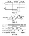
- FIGURE 3 is a timing diagram illustrating proper setup and hold times.
- FIGURE 4 is a schematic diagram of the synchronization process according to the present invention.
- FIGURE 5 is a schematic diagram of a simple synchronizing clock generator according to the present invention.
- FIGURE 6 is a timing diagram for the circuit of Figure 4.
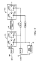
- FIGURE 7 is a schematic diagram of the process according to the present invention wherein the original net list contains latches instead of flip-flops.
- FIGURE 8 is a timing diagram for the circuit of Figure 7.
- a user net list is a text description of any digital sequential logic circuit.
- a user net list typically may specify a plurality of D type flip-flops 10a, 10b,... 10n. It is to be understood by those of ordinary skill in the art that each user flip-flop 10a, 10b,... 10n is representative of all such user flip-flops as may be used to configure various sequential logic in the user net list. For representative purposes, each user flip-flop 10a, 10b,... 10n is shown as a D type flip-flop having a data input D, a clock input for receiving a clock signal and a data output Q. Although those of ordinary skill in the art well recognize that the present invention may be used with other clocked elements.
- Each user flip-flop 10a, 10b,...10n is also associated with a corresponding combinational logic unit 14a, 14b,...14n. Data propagates through the combinational logic in accordance with conventional methods, and the output of each logic unit is clocked into corresponding flip-flop devices 16a, 16b,...16n.
- Figure 2 shows an example of an unsynchronized logic circuit implemented directly from a user net list.
- Data must be present at the data input D of the user's original flip-flops 18 and 20 before the arrival of a clock signal over line 28 to the clock inputs 22 and 24 of the original flip-flops 18 and 20.
- the output Q of original flip-flop 18 is connected to the data input D of the original flip-flop 20.
- a delay element 26 is shown on the clock line 28 to illustrate the effect of skew in the clock line.
- the timing diagram of Figure 3 shows that in order for an implemented logic circuit to operate properly, data must be stable on the input D of a flip-flop device relative to the arrival of the clock pulse at the clock input for a specified period of time.
- t s for any clocked device there is a specified "setup time” t s and also a specified “hold time” t h .
- Input data must be present and stable from at least t s before the clock transition until a period equal to at least t h after the clock transition for proper operation.
- t s might be equal to 20 nanoseconds and t h equal to 5 nanoseconds. That is, the setup time requirement is met if the data input has been stable for at least 20 nanoseconds before the next clock rising edge.
- a synchronizer flip-flop 30a, 30b is provided for each corresponding user original flip-flop 10a, 10b specified by the user net list.
- Each synchronizer flip-flop 30a, 30b is a "shadow" flip-flop which is provided upstream in the data path relative to each of the corresponding original user flip-flops 10a, 10b.
- Each synchronizer flip-flop 30a, 30b includes a data input D, a data output Q and a clock input 32a, 32b, respectively.
- each original user flip-flop 10a, 10b has a data input D, a data output Q and a clock input 34a, 34b, respectively.
- Clock skew which inherently occurs in a practical realization of the design is schematically represented by delay elements 36a, 36b.
- Figure 4 shows only two original user flip-flops 10a, 10b, and two synchronizer flip-flops 30a, 30b for the sake of simplicity. It will be appreciated that in an actual implementation according to the present invention, there is no limit to the number of flip-flop devices which may be synchronized.
- the synchronization method In order to achieve the precise synchronization of data and clock signals necessary to successfully implement a user's net list, the synchronization method must insure that the synchronizer flip-flops 30a, 30b, receive and properly clock in data on their respective inputs along data lines 38b, 38c before the original flip-flops 10a, 10b receive data. This is done by adding a certain amount of delay in the external data line 38a.
- the means 40 for providing the delay may be a series of inverters or other known means for delaying a signal.
- the amount of delay is chosen by first determining the amount of skew in the user original net list.
- the amount of skew may be empirically determined in accordance with conventional techniques.
- each synchronizer 30a, 30b must arrive at the respective clock input 32a, 32b of each synchronizer 30a, 30b before the user's clock arrives at the clock input of each user flip-flop 10a, 10b.
- a delay means 42 is provided in each clock line 44, in order to delay the arrival of the clock signal to the clock input 34a, 34b of the user's original flip-flop devices 10a, 10b.
- Delay means 42 may be any convenient means for delaying the arrival of the clock signal.
- a simple synchronizing clock generator 46 is provided for deriving a synchronizing clock from each original user clock on the same frame of reference.
- the present synchronization method works for multiple nonoverlapping user clocks, that is, a plurality of user clocks on the same frame of reference. All that is needed is that multiple clocks on the same frame of reference be gated into an OR gate (not shown) which has multiple input leads and a single output lead before being applied to the synchronizing flip-flop.
- the output of the OR gate would provide the clock on line 42a as shown in Figure 4.
- a simple synchronizing clock generator 46 may be provided which derives a synchronizing clock to be applied to the clock input leads 32a, 32b of a corresponding synchronizer 30a, 30b.
- a synchronizing clock is generated from each user clock independently.
- the individual synchronizing clocks are then gated together by an OR gate. Care must be taken that the edges do not occur too close together as this would cause the synchronizing clocks to overlap.
- synchronizing clock generator 46 comprises an Exclusive OR gate 50 having a first input 52, a second input 54 and an output 56.
- Input 52 is connected to the user's clock through a delay means 58.
- Delay means 58 may be any suitable means such as a series of inverters for introducing delay into the clock signal.
- the second input 54 of the Exclusive OR gate 50 is connected directly to the user's clock signal.
- the synchronizing clock signal (the output of Exclusive OR gate 50) is applied through the output 56 of the Exclusive OR gate 50 in the synchronizing clock generator 46 to the clock inputs 32a, 32b of the synchronizers 30a, 30b.
- the method according to the present invention provides an implemented circuit consisting of fully synchronized flip-flop devices FF1 and FF2.
- the implemented circuit is a fully synchronized version of the circuit specified by the user's original net list.
- the synchronizer flip-flops 30a, 30b and the user's original flip-flop devices 10a, 10b together comprise synchronized flip-flop devices FF1, FF2 which will allow the circuit to work correctly regardless of the inevitable and unpredictable clock skew provided that the delay elements 40, and 42 are chosen correctly.
- the sequential operation of the circuit shown in Figure 4 may be understood by referring to the timing diagram in Figure 6.
- the circuit operates correctly when the input data 38a is latched by the rising edge of the clock 44 in the user's original flip-flop 10a. Data is saved in flip-flop 10a until the next rising clock edge when it is passed through combinatorial logic 21 and latched into the user's original flip-flop 10b. Without the synchronization flip-flops 30a, 30b, the inherent clock skew will move the rising edge of the clock signal at the clock inputs of some flip-flops, 10b for example, outside of the region where data on the input lead is valid.
- the synchronizing clock at clock inputs 32a, 32b of synchronizer flip-flops 30a, 30b is generated from the clock signal 44. Skew between the clock or control inputs at different synchronizer flip-flops is indicated by double rising and falling lines in the timing diagram. Similarly, the delayed clock signal at the clock inputs 34a, 34b to the user's original flip-flops 10a, 10b is shown with multiple rising and falling lines to indicate the skew between different inputs.
- the synchronized circuit operates as follows. First, the input data 38a is delayed to produce waveform 38b. It is then latched in synchronizer flip-flop 30a by the rising edge of the synchronizing clock signal.
- the delay element 40 must provide sufficient delay to ensure that the data is valid at the rising edge of the synchronizing clock despite delay and skew in the synchronizing clock signal. It may not be necessary in some implementations. Width of the synchronizing clock signal is not important as long as it is sufficient to meet the pulse width requirements of flip-flops 30a, 30b. After the valid data is saved in synchronizer flip-flop 30a, it is transferred to the user's original flip-flop 10a and saved by the rising edge of the delayed clock signal 34a, 34b.
- the clock signal must be delayed sufficiently to ensure that the time is provided from the rising edge of the synchronizing clock for data to propagate through synchronizer flip-flop 30a and be present at the input of flip-flop 10a despite skew in the synchronizing clock signal.
- Data then propagates through combinational logic 21 and is saved in synchronizer flip-flop 30b by the next synchronizing clock.
- the synchronizing clock signal is generated on both the rising and falling edge of the clock 44 in case some of the user's original flip-flops are falling edge triggered instead of rising edge triggered.
- the present invention provides fully synchronized flip-flop devices FF1 and FF2 in the implemented circuit as shown in Figure 4.
- the implemented circuit may thus be viewed as a synchronized implemented user net list.
- the synchronization method according to the present invention provides a method for automatically synchronizing a user net list without taking into account the amount of clock skew in the implemented circuit.
- the present invention provides a significant advantage over the prior art in that it produces a fully synchronized implemented circuit even in the presence of large amounts of clock skew which may exist in the circuit being implemented.
- the present invention provides automatic data synchronization in an implemented circuit without violating hold time and setup constraints, even in the presence of clock skew.
- the present invention has the advantage of enabling a user to implement a design from a user net list without the expense of having to first manually implement and test the design in order to eliminate hold time violations. It will be appreciated that the automatic method of data synchronization according to the present invention provides considerable time savings in comparison with prior art techniques for implementing a complete circuit design from a user net list.
- the previously described embodiment of the present invention is not applicable if the user's original net list contains transparent latches in addition to, or instead of edge triggered flip-flops. Circuits containing transparent latches often rely on the characteristic that data will be transferred through the latch as long as the control or clock input is active. If a synchronizer flip-flop is placed in front of a transparent latch, data will be transferred on the rising edge of the synchronizing clock signal and will be blocked at other times.
- FIG. 7 An alternate embodiment of the present invention which may be used for circuits containing transparent latches is illustrated with reference to Figure 7.
- Figure 7 is the same as Figure 4 except that the user's original flip-flop devices 10a, 10b and the synchronizing flip-flops 30a, 30b are replaced by transparent latches 64a, 64b and 66a, 66b, respectively.
- the synchronizer latches 66a, 66b have active low control inputs 68a, 68b so that they transfer data as long as the synchronizing clock from the synchronizing clock generator 46 is low and block data when the synchronizing clock is high.
- the synchronizing clock signal may be inverted and active high synchronizer latches used.
- FIG 8. A timing diagram for the circuit of Figure 7 is shown in Figure 8.
- the synchronizing clock is generated by synchronizing clock generator 46 as previously explained, except that the pulse width must be controlled so that the falling edge of the synchronizing clock occurs after the rising or falling edge of the delayed clock for-all sequential logic elements despite the clock skew illustrated by delay 20 in the clock line of Figure 7.
- the operation of this circuit may be understood by thinking of the synchronizing clock as a blocking signal which prevents data from being transferred through the user's original latches during the skew period on the delayed clock signal. It is not desirable to make the width of the synchronizing clock too long as this will directly affect the maximum speed of operation of the synchronized circuit.
- the width of the synchronizing clock is adjusted by first determining the amount of skew in the synchronizing clock net and in the user clock net. Then, the width of the synchronizing clock is set so the falling edge at the synchronizing latch occurs after the rising or falling edge of the user clock at the corresponding original user latch for all latches in the original user net list.
- the synchronizing technique using transparent latches as synchronizing elements may be used if the user's original sequential devices were either edge triggered flip-flops or transparent latches.
- the synchronizing technique using edge triggered flip-flops as synchronizing elements may be used only if the user's original sequential devices were edge triggered flip-flops.
- a design containing a mixture of transparent latches and edge triggered flip-flops may be synchronized using transparent latches as synchronizing elements or by using a mixture of transparent latches and edge triggered flip-flops as synchronizing elements.
Landscapes
- Engineering & Computer Science (AREA)
- Theoretical Computer Science (AREA)
- Physics & Mathematics (AREA)
- Computer Hardware Design (AREA)
- General Engineering & Computer Science (AREA)
- General Physics & Mathematics (AREA)
- Evolutionary Computation (AREA)
- Geometry (AREA)
- Synchronisation In Digital Transmission Systems (AREA)
Applications Claiming Priority (2)
| Application Number | Priority Date | Filing Date | Title |
|---|---|---|---|
| US51069890A | 1990-04-18 | 1990-04-18 | |
| US510698 | 1990-04-18 |
Publications (2)
| Publication Number | Publication Date |
|---|---|
| EP0453171A2 true EP0453171A2 (fr) | 1991-10-23 |
| EP0453171A3 EP0453171A3 (en) | 1992-11-19 |
Family
ID=24031805
Family Applications (1)
| Application Number | Title | Priority Date | Filing Date |
|---|---|---|---|
| EP19910303169 Withdrawn EP0453171A3 (en) | 1990-04-18 | 1991-04-10 | Method for substantially eliminating hold time violations in implementing high speed logic circuits or the like |
Country Status (2)
| Country | Link |
|---|---|
| EP (1) | EP0453171A3 (fr) |
| JP (1) | JPH04227576A (fr) |
Cited By (8)
| Publication number | Priority date | Publication date | Assignee | Title |
|---|---|---|---|---|
| EP0559322A3 (fr) * | 1992-01-31 | 1995-06-14 | Pie Design Systems Inc | |
| FR2724472A1 (fr) * | 1994-09-14 | 1996-03-15 | Suisse Electronique Microtech | Automate insensible aux delais d'horloge |
| EP0706107A1 (fr) * | 1994-10-03 | 1996-04-10 | International Business Machines Corporation | Méthode et dispositif de cadencement de réseau pour sous-systèmes d'entrées/sorties |
| US5649176A (en) * | 1995-08-10 | 1997-07-15 | Virtual Machine Works, Inc. | Transition analysis and circuit resynthesis method and device for digital circuit modeling |
| EP0924859A1 (fr) * | 1997-12-18 | 1999-06-23 | Advanced Micro Devices, Inc. | Circuit logique avec génération d'horloge propre et procédé associé |
| EP0818786A3 (fr) * | 1996-07-09 | 1999-12-01 | Siemens Aktiengesellschaft | Circuit CMOS composé de blocs de circuits CMOS arrangés selon des routes de données parallèles aux directions des bits |
| US6377912B1 (en) | 1997-05-30 | 2002-04-23 | Quickturn Design Systems, Inc. | Emulation system with time-multiplexed interconnect |
| WO2006075206A3 (fr) * | 2005-01-12 | 2006-09-08 | Nokia Corp | Circuit diviseur d'horloge numerique |
Family Cites Families (1)
| Publication number | Priority date | Publication date | Assignee | Title |
|---|---|---|---|---|
| EP0461291A1 (fr) * | 1990-06-15 | 1991-12-18 | International Business Machines Corporation | Génération de signaux d'horloge dans un système d'ordinateur à multi-puces |
-
1991
- 1991-04-10 EP EP19910303169 patent/EP0453171A3/en not_active Withdrawn
- 1991-04-17 JP JP3112623A patent/JPH04227576A/ja active Pending
Cited By (13)
| Publication number | Priority date | Publication date | Assignee | Title |
|---|---|---|---|---|
| US5475830A (en) * | 1992-01-31 | 1995-12-12 | Quickturn Design Systems, Inc. | Structure and method for providing a reconfigurable emulation circuit without hold time violations |
| US5649167A (en) * | 1992-01-31 | 1997-07-15 | Quickturn Design Systems, Inc. | Methods for controlling timing in a logic emulation system |
| EP0559322A3 (fr) * | 1992-01-31 | 1995-06-14 | Pie Design Systems Inc | |
| FR2724472A1 (fr) * | 1994-09-14 | 1996-03-15 | Suisse Electronique Microtech | Automate insensible aux delais d'horloge |
| EP0706107A1 (fr) * | 1994-10-03 | 1996-04-10 | International Business Machines Corporation | Méthode et dispositif de cadencement de réseau pour sous-systèmes d'entrées/sorties |
| US5649176A (en) * | 1995-08-10 | 1997-07-15 | Virtual Machine Works, Inc. | Transition analysis and circuit resynthesis method and device for digital circuit modeling |
| US6009531A (en) * | 1995-08-10 | 1999-12-28 | Ikos Systems, Inc. | Transition analysis and circuit resynthesis method and device for digital circuit modeling |
| EP0818786A3 (fr) * | 1996-07-09 | 1999-12-01 | Siemens Aktiengesellschaft | Circuit CMOS composé de blocs de circuits CMOS arrangés selon des routes de données parallèles aux directions des bits |
| US6377912B1 (en) | 1997-05-30 | 2002-04-23 | Quickturn Design Systems, Inc. | Emulation system with time-multiplexed interconnect |
| EP0924859A1 (fr) * | 1997-12-18 | 1999-06-23 | Advanced Micro Devices, Inc. | Circuit logique avec génération d'horloge propre et procédé associé |
| US6064232A (en) * | 1997-12-18 | 2000-05-16 | Advanced Micro Devices, Inc. | Self-clocked logic circuit and methodology |
| WO2006075206A3 (fr) * | 2005-01-12 | 2006-09-08 | Nokia Corp | Circuit diviseur d'horloge numerique |
| US7653168B2 (en) | 2005-01-12 | 2010-01-26 | Nokia Corporation | Digital clock dividing circuit |
Also Published As
| Publication number | Publication date |
|---|---|
| EP0453171A3 (en) | 1992-11-19 |
| JPH04227576A (ja) | 1992-08-17 |
Similar Documents
| Publication | Publication Date | Title |
|---|---|---|
| US5259006A (en) | Method for substantially eliminating hold time violations in implementing high speed logic circuits or the like | |
| US5087828A (en) | Timing circuit for single line serial data | |
| US5900753A (en) | Asynchronous interface | |
| US6353906B1 (en) | Testing synchronization circuitry using digital simulation | |
| US8819472B1 (en) | Method and system for clock edge synchronization of multiple clock distribution integrated circuits by configuring master device to produce at least one gated clock output signal | |
| CN113608600B (zh) | 具有多个时钟域和复位域的系统中数据同步的方法和设备 | |
| US4419629A (en) | Automatic synchronous switch for a plurality of asynchronous oscillators | |
| US7284143B2 (en) | System and method for reducing clock skew | |
| EP0319187A2 (fr) | Couplage de chemin de données de test | |
| Wagner | Clock system design | |
| EP0453171A2 (fr) | Méthode pour éliminer substantiellement les violations de temps de maintien dans la mise en oeuvre de circuits logiques à grande vitesse ou similaires | |
| EP1116087B1 (fr) | Systeme de repartition d'horloge polyphase et synchrone | |
| US6982575B2 (en) | Clock ratio data synchronizer | |
| US6711089B2 (en) | Method and apparatus for performing signal synchronization | |
| US6304125B1 (en) | Method for generating and distribution of polyphase clock signals | |
| US20020166003A1 (en) | Method and apparatus for a failure-free synchronizer | |
| CN117435016A (zh) | 一种复位电路的设计方法 | |
| US7333516B1 (en) | Interface for synchronous data transfer between domains clocked at different frequencies | |
| US4912340A (en) | Circuit for generating non-overlapping two-phase clocks | |
| US6928574B1 (en) | System and method for transferring data from a lower frequency clock domain to a higher frequency clock domain | |
| US8564337B2 (en) | Clock tree insertion delay independent interface | |
| US4789959A (en) | Delay circuit for a real time clock | |
| US6931562B1 (en) | System and method for transferring data from a higher frequency clock domain to a lower frequency clock domain | |
| USH1796H (en) | Method and circuit for eliminating hold time violations in synchronous circuits | |
| US5912573A (en) | Synchronizing clock pulse generator for logic derived clock signals for a programmable device |
Legal Events
| Date | Code | Title | Description |
|---|---|---|---|
| PUAI | Public reference made under article 153(3) epc to a published international application that has entered the european phase |
Free format text: ORIGINAL CODE: 0009012 |
|
| AK | Designated contracting states |
Kind code of ref document: A2 Designated state(s): DE FR GB |
|
| PUAL | Search report despatched |
Free format text: ORIGINAL CODE: 0009013 |
|
| AK | Designated contracting states |
Kind code of ref document: A3 Designated state(s): DE FR GB |
|
| 17P | Request for examination filed |
Effective date: 19930422 |
|
| RAP1 | Party data changed (applicant data changed or rights of an application transferred) |
Owner name: QUICKTURN DESIGN SYSTEMS, INC. |
|
| 17Q | First examination report despatched |
Effective date: 19970513 |
|
| STAA | Information on the status of an ep patent application or granted ep patent |
Free format text: STATUS: THE APPLICATION IS DEEMED TO BE WITHDRAWN |
|
| 18D | Application deemed to be withdrawn |
Effective date: 19970924 |