EP0453191A2 - Circuit translateur logique - Google Patents
Circuit translateur logique Download PDFInfo
- Publication number
- EP0453191A2 EP0453191A2 EP91303252A EP91303252A EP0453191A2 EP 0453191 A2 EP0453191 A2 EP 0453191A2 EP 91303252 A EP91303252 A EP 91303252A EP 91303252 A EP91303252 A EP 91303252A EP 0453191 A2 EP0453191 A2 EP 0453191A2
- Authority
- EP
- European Patent Office
- Prior art keywords
- cml
- ttl
- transistor
- input
- schottky diode
- Prior art date
- Legal status (The legal status is an assumption and is not a legal conclusion. Google has not performed a legal analysis and makes no representation as to the accuracy of the status listed.)
- Withdrawn
Links
- 238000013519 translation Methods 0.000 claims abstract description 21
- 230000000295 complement effect Effects 0.000 claims description 9
- 238000010586 diagram Methods 0.000 description 4
- 238000012545 processing Methods 0.000 description 4
- 230000009467 reduction Effects 0.000 description 3
- 230000001052 transient effect Effects 0.000 description 3
- 230000036039 immunity Effects 0.000 description 2
- 238000002955 isolation Methods 0.000 description 2
- 238000012986 modification Methods 0.000 description 2
- 230000004048 modification Effects 0.000 description 2
- 230000002411 adverse Effects 0.000 description 1
- 230000008859 change Effects 0.000 description 1
- 230000007423 decrease Effects 0.000 description 1
- 230000001934 delay Effects 0.000 description 1
- 238000013461 design Methods 0.000 description 1
- 230000000694 effects Effects 0.000 description 1
- 230000006872 improvement Effects 0.000 description 1
- 239000000463 material Substances 0.000 description 1
- 230000000630 rising effect Effects 0.000 description 1
- 239000004065 semiconductor Substances 0.000 description 1
- 238000012546 transfer Methods 0.000 description 1
Images

Classifications
-
- H—ELECTRICITY
- H03—ELECTRONIC CIRCUITRY
- H03K—PULSE TECHNIQUE
- H03K19/00—Logic circuits, i.e. having at least two inputs acting on one output; Inverting circuits
- H03K19/0175—Coupling arrangements; Interface arrangements
- H03K19/018—Coupling arrangements; Interface arrangements using bipolar transistors only
- H03K19/01806—Interface arrangements
- H03K19/01812—Interface arrangements with at least one differential stage
Definitions
- This invention relates generally to logic level translators and more particularly, it relates to a logic translator circuit for converting transistor-transistor-logic (TTL) level signals to current-mode-logic (CML) level signals which may have a higher speed of operation, a reduction in power dissipation and immunity from ground bounce noise.
- TTL transistor-transistor-logic
- CML current-mode-logic
- TTL one logic type
- CML/ECL another logic type
- TTL logic circuits typically operate on logic signal levels below +0 ⁇ .8 volts and above +2.0 ⁇ volts while CML logic circuits typically operate on different logic levels between -1.0 ⁇ to -1.6 volts. While the precise levels utilized in the CML/ECL logic circuits differ among manufacturers, the voltage swing between the two CML logic levels is commonly less than the voltage swing between the two TTL logic levels. Further, the TTL circuit makes use of a positive power source voltage VCC (i.e., +5.0 ⁇ volts) and a ground potential TGND). On the other hand, the CML circuit makes use of a negative power supply voltage VEE (i.e., -5.2 volts) and a ground potential CGND). Both ground potentials TGND and CGND are typically at zero volts.
- VCC positive power source voltage
- VEE negative power supply voltage
- Prior art translators use diodes and other semi-conductor devices to obtain a fixed voltage drop to translate from one type of binary signal level to another type of binary signal level.
- these prior art translators suffer from the disadvantage in that they used a common ground which is shared by both the TTL input and CML output signals.
- the TTL input signals and the CML output signals would share the same bus line as a common ground.
- Such a logic level translator 10 of the prior art is shown in Figure 1 and has been labeled "Prior Art.” This prior art translator can be found in "Analysis and Design of Digital Integrated Circuits" written by David A. Hodges and Horace G. Jackson, p. 296, published in 1983 by McGraw-Hill, Inc.
- This prior art translator 10 includes a TTL input stage 12 and a CML output stage 14.
- the TTL input stage 12 is coupled between a positive power supply voltage VCC (i.e., +5.0 ⁇ volts) and a ground potential GND.
- the TTL input stage 12 receives TTL logic levels at input nodes A and B.
- the CML output stage 14 is coupled between a negative power supply potential VEE (i.e., -5.2 volts) and the same ground potential (GND).
- VEE negative power supply potential
- the CML output stage 14 can deliver both an OR output at the collector of the transistor Q5 and a NOR output at the collector of the transistor Q4.
- any TTL currents flowing in the commonly shared ground bus (GND) will produce noise signals (referred to as ground bounce noise) in the CML output stage 14 of the translator.
- any variations in the positive power supply potential VCC used in the TTL input stage 12 would be coupled to the CML output stage 14 of the translator.
- the input threshold of the TTL input stage depends directly on the value of the voltage V R at the base of the transistor Q5 and the value of the voltage V BB at the base of the transistor Q2.
- the use of a resistor R3 to perform a level shifting limits the transient current, thereby causing propagation delays which reduces the speed of operation of the translator.
- a logic level translator circuit represents an improvement over the translator circuit 10 of Figure 1 which isolates the TTL and CML ground bus lines so as to reduce the noise that may be transferred between the TTL ground bus and the CML ground bus.
- TTL-to-CML translator circuit which provides isolation between a TTL ground bus and a CML ground bus so as to reduce the noise that may be transferred there-between.
- TTL-to-CML translator circuit which includes a TTL input transistor, a translation chain, a first CML differential pair, a level shifter, and a second CML differential pair.
- the present invention is concerned with the provision of a logic translator circuit for converting TTL logic level signals into CML logic level signals which includes a TTL input transistor, a translation chain, a first CML differential pair, a level shifter, and a second CML differential pair.
- the TTL input transistor has its base coupled to an input terminal for receiving TTL logic level signals, its collector connected to a positive power supply potential, and its emitter connected to an output node.
- the translation chain is formed of a plurality of series-connected diodes. One end of the translation chain is connected to the output node.
- the first CML differential pair is formed of first and second input transistors having their emitters connected together.
- the first input transistor has its collector connected to a TTL ground potential via a first load resistor and its base connected to the other end of the translation chain.
- the second input transistor has its collector connected to the TTL ground potential via a second load resistor and its base connected to a reference potential.
- a first current source is connected between the common emitters of the first and second input transistors and a negative supply potential.
- a level shifter is formed of first and second emitter follower transistors.
- the first emitter follower transistor has its collector connected to the TTL ground potential and its base connected to the collector of the second input transistor.
- the second emitter follower transistor has its collector connected to the TTL ground potential and its base connected to the collector of the first input transistor.
- the second CML differential pair is formed of third and fourth input transistors having their emitters connected together.
- the third input transistor has its collector connected to a CML ground potential via a third load resistor and its base coupled to the emitter of the second emitter follower transistor.
- the CML ground potential is electrically isolated from the TTL ground potential.
- the fourth input transistor has its collector connected to the CML ground potential via a fourth load resistor and its base coupled to the emitter of the first emitter follower transistor.
- a second current source is connected between the common emitters of the third and fourth input transistors and the negative supply potential.
- the collector of the third input transistor is connected to a first output terminal for providing a true CML logic level signal
- the collector of the fourth input transistor is connected to a second output terminal for providing a complementary CML logic level signal.
- FIG. 1 a schematic circuit diagram of a conventional prior art TTL-to-CML translator device 10 which is used for converting TTL logic level signals to CML-compatible logic level signals.
- the translator device 10 is comprised of a TTL input stage 12, a level shifter 13, a CML output stage 14 and a reference voltage generator circuit 16.
- the TTL input stage 12 consists of diodes D1, D2, D8, D9; resistors R1, R2; and a transistor Q1.
- the input stage 12 is coupled between a positive power supply potential VCC (+5.0 ⁇ volts) and a ground potential GND on a ground bus line 18.
- the input stage receives TTL-level data input signals V in1 and V in2 respectively on its nodes A and B.
- the level shifter 13 is formed of diodes D3-D5; resistors R3, R4, R5; and transistors Q2, Q3.
- the CML/ECL output stage 14 includes an output differential pair formed of transistors Q4, Q5; a current source formed of a transistor Q6 and a resistor R6; load resistors R7, R8; and emitter follower transistors Q9, Q10.
- the output stage is coupled between a negative power supply potential VEE (-5.2 volts) and the same ground potential GND on the common bus line 18.
- VEE negative power supply potential
- a CML-level output voltage V out1 representing the AND logic of the two input signals V in1 and V in2 appears at collector of the transistor Q5.
- a corresponding ECL-level output voltage V out2 appears at the emitter of the transistor Q10.
- a CML-level output signal V out3 representing the NAND logic of the two input signals at V in1 and V in2 appear at the collector of the transistor Q4.
- a corresponding ECL-level output signal V out4 appears at the emitter of the transistor Q9.
- the reference voltage generator circuit 16 includes diodes D6, D7; resistors R9-R13; and transistors Q7, Q8.
- a first reference voltage V R is provided at the junction of the emitter of the transistor Q7 and the base of the transistor Q5.
- a second reference voltage V CS is provided at a junction of the emitter of the transistor Q8 and the base of the transistor Q6.
- a third reference voltage V BB is provided at the junction of the anode of the diode D6 and the bases of the transistors Q2 and Q8.
- ground bus line 18 is shared by the TTL input stage 12 and the CML output stage 14.
- the switching of the two input signals V in1 and V in2 in the input stage 12 may cause current spikes or noise to appear on the common ground bus line 18, sometimes referred to as "ground bounce noise.”
- this noise will be transferred to the CML output stage 16 which will adversely affect the CML-level output signals.
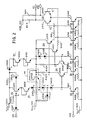
- FIG. 2 of the drawings there is shown a schematic circuit diagram of a TTL-to-CML translator device 110 which is constructed in accordance with the principles of the present invention.
- the translator device 110 is comprised of a TTL input stage 20, a translator chain 22, a first CML differential pair 24, a level shifter 26, and a second CML differential pair 28.
- the translator device 110 further includes a plurality of constant current sources 30-40.
- a TTL level signal applied to input terminal Din is converted or translated into a CML level signal at output terminals D1 and D1B. It will be noted that the TTL ground GTTL and the CML ground GCML are isolated by the level shifter 26.
- this isolation between the TTL ground and the CML ground coupled with the use of the second CML differential pair 28 serves to greatly reduce any noise that appears on the TTL ground bus GTTL from being transferred to the CML ground bus GCML.
- this translation device 110 is capable of producing relatively noise free CML-compatible output signals at the output terminals D1 and D1B.
- the TTL input stage 20 is formed of an input transistor Q401, a Schottky diode D407, and a resistor R401.
- the transistor Q401 has its collector connected to a positive power supply potential VTTL, which is typically at +5.0 ⁇ volts.
- the base of the transistor Q401 is connected to the anode of the Schottky diode D407 and to one end of the resistor R401.
- the other end of the resistor R401 is also connected to the positive supply potential VTTL.
- the cathode of the diode D407 is connected to the input terminal Din.
- the translation chain 22 is formed of a diode-connected transistor Q409 and Schottky diodes D401, D404, and D405.
- the emitter of the transistor Q401 is connected to the base-to-collector terminal of the transistor Q409.
- the emitter of the transistor Q409 is tied to the anode of the diode D401.
- the cathode of the diode D401 is tied to the anode of the diode D404.
- the cathode of the diode D404 is joined to the anode of the diode D405.
- the cathode of the diode D405 is joined to the base of an input transistor Q405 in the first differential pair 24 and to the current source 30.
- the current source 30 is formed of a transistor Q411 and a resistor R405.
- the transistor Q411 has its collector also connected to the base of the transistor Q405, its base connected to a reference voltage VCS, and its emitter connected to one end of the resistor R405.
- the other end of the resistor R405 is connected to a negative power supply potential VEE, which is typically at -5.2 or -4.5 volts.
- the first CML or translator differential pair 24 includes the first input transistor Q405 and a second input or reference transistor Q406, and load resistors R403, R404.
- the input transistor Q405 has its collector connected to one end of the load resistor R403, and the second input transistor Q406 has its collector connected to one end of the load resistor R404.
- the other ends of the resistors R403 and R404 are connected to a TTL ground bus line GTTL which is typically at zero volts.
- the emitters of the input transistors Q405 and Q406 are connected together and to the current source 32.
- the current source 32 is formed of a transistor Q412 and a resistor R406.
- the transistor Q412 has its collector connected to the common emitters of the input transistors Q405 and Q406, its base connected to the reference voltage VCS, and its emitter connected to one end of the resistor R406. The other end of the resistor R406 is connected to the negative power supply potential VEE.
- a reference generator formed by a pair of series-connected Schottky diodes D406 and D409 is interconnected between the TTL ground bus line GTTL and the base of the second input transistor Q406.
- the anode of the diode Q409 is connected to the bus line GTTL
- the cathode of the diode D406 is connected to the base of the transistor Q406.
- the diodes D406 and D409 are selected so that their operating characteristics are substantially identical to the diodes D404 and D405.
- the cathode of the diode D406 is also connected to the current source 34.
- the current source 34 is identical to the current source 30 so as to eliminate matching errors and is formed of a transistor Q413 and a resistor R407.
- the transistor Q413 has its collector connected to the base of the transistor Q406, its base connected to the reference voltage VCS, and its emitter connected to one end of the resistor R407. The other end of the resistor R407 is connected to the negative power supply potential VEE.
- a reference voltage V REF will be developed at the base (node A) of the second input transistor Q406 which is approximately 1.0 ⁇ volts below the bus line GTTL or -1.0 ⁇ volts. Thus, this will also be the trip voltage on the base (node C) of the first input transistor Q405. Further, the voltage at the node B will be at zero volts or virtual ground since the voltage V B is two Schottky diode drops above the voltage V C at the base of the transistor Q405 and is given by:
- threshold voltage V TH at the input terminal Din is referenced to the TTL ground bus line GTTL and is calculated to be equal to 2V BE as follows: Since there is no resistor in the translation chain 22, such as the resistor R3 in the prior art of Figure 1, there is achieved a higher speed of operation. This higher speed is obtained by eliminating of this resistor R3 which will allow the current in the translation chain 22 not to be limited, and all of this current will be available to charge/discharge the capacitance at the base of the input transistor Q405. Moreover, this serves to reduce the amount of power dissipation.
- the level shifter 26 consists of a first emitter follower transistor Q417, a first emitter resistor R412, a second emitter follower transistor Q418, and a second emitter resistor R411.
- the transistor Q417 has its collector connected to the TTL ground bus line GTTL, its base connected to the collector of the transistor Q406 and its emitter connected to one end of the resistor R412.
- the other end of the resistor R412 is connected to the current source 36.
- the current source 36 is formed of a transistor Q414 and a resistor R408.
- the transistor Q414 has its collector connected to the other end of the resistor R412, its base connected to the reference voltage VCS, its emitter connected to one end of the resistor R408.
- the other end of the resistor R408 is connected to the negative power supply potential VEE.
- the transistor Q418 has its collector connected to the TTL ground bus line GTTL, its base connected to the collector of the transistor Q405, and its emitter connected to one end of the resistor R411.
- the other end of the resistor R411 is connected to the current source 38.
- the current source 38 is formed of a transistor Q415 and a resistor R409.
- the transistor Q415 has its collector connected to the other end of the resistor R411, its base connected to the reference voltage VCS, and its emitter connected to one end of the resistor R409.
- the other end of the resistor R409 is connected to the negative power supply potential VEE.
- the transistor Q417 and the resistor R412 acts as a buffer and level shifts the voltage at the collector (node E) of the transistor Q406 to a new voltage V1 at node K.
- This voltage V1 is applied to the base of the input transistor Q420 in the second CML differential pair 28.
- the transistor Q418 and the resistor R411 serves as a buffer and level shifts the voltage at the collector (node F) of the transistor Q405 to a new voltage V2 at node J.
- the voltage V2 is applied to the base of the transistor Q419 in the second CML differential pair.
- the common-mode voltage of voltages V1 and V2 (their center value) is centered between its maximum allowable range which is dictated by the saturation of the switching transistors Q419, Q420 or the current source transistor Q416. This scheme will allow for the maximum change in the common-mode voltage of V1 and V2 (which is really simply the difference between the ground potentials GTTL and GCML). The ground bounce noise occurring on the TTL ground bus line GTTL is added to both the voltages V1 and V2.
- the second CML differential pair 28 which responds to the difference between the values of the voltages V1 and V2, and separating the ground potentials GTTL and GCML, the effect of the ground bounce noise have been eliminated from the CML ground bus line GCML and the output terminals D1 and D1B.
- the second CML or output differential pair 28 is comprised of input transistors Q419 and Q420 and load resistors R413 and R414.
- the input transistor Q419 has its collector connected to one end of the resistor R413 and to the output terminal D1 for providing a true CMLcompatible signal.
- the input transistor Q420 has its collector connected to one end of the resistor R414 and to the output terminal D1B for providing a complementary CML-compatible signal.
- the other ends of the resistors R413 and R414 are connected to the CML ground bus line GCML.
- the emitters of the transistors Q419 and Q420 are connected together and to the current source 40.
- the current source 40 is formed of a transistor Q416 and a resistor R410.
- the transistor Q416 has its collector connected to the common emitters of the input transistors Q419 and Q420, its base connected to the reference voltage VCS, and its emitter connected to one end of the resistor R410. The other end of the resistor R410 is connected to the negative power supply potential VEE.
- the translator device 110 further includes an input clamp circuit 42 formed of a pair of Schottky diodes D402, D403 and a pair of diode-connected transistors Q404, Q410, and a resistor R402.
- the clamp circuit 42 serves to limit the upper boundary on the voltage at the base of the input transistor Q401 or node D from rising above 2V SH + 2V BE . Consequently, the voltages at the corresponding nodes D, B and H can only go positive by one Schottky voltage drop V SH relative to their threshold values.
- a swing clamp 44 is formed of a clamping transistor Q402 and a clamping diode D408.
- the clamping transistor Q402 is provided to limit the voltage between the TTL ground bus line GTTL and the node B.
- the transistor Q402 has its base and collector connected to the TTL ground bus line GTTL and its emitter connected to the node B.
- the clamping diode D408 serves to limit the transient voltage at the Node H with respect to the TTL ground bus line GTTL.
- the anode of the diode D408 is connected to the node H, and the cathode of the diode D408 is connected to the TTL ground bus line GTTL.
- the travel at the nodes H and C will be definitely clamped to one Schottky diode drop V SH in the positive direction and one V BE drop in the negative direction from their threshold values. Therefore, since the swing at the node C is minimized, a higher speed of operation is achieved.
- the clamping diode D408 is only a transient clamp, and the clamp circuit 42 will act to limit the swing in the positive direction on a DC basis.
- the transistor Q405 Since the transistor Q405 is non-conductive, the voltage at node F will be zero volts, which will produce a higher-than threshold voltage at the node J. Further, since the voltage at the base (node J) of the transistor Q419 will be less negative than the voltage at the base (node K) of the transistor Q420, the transistor Q419 will be turned on and the transistor Q420 will be turned off. The voltage drop across the resistor R413 will provide a voltage of approximately -0 ⁇ .350 ⁇ volts at the collector of the transistor Q419 or the output terminal D1 which represents a binary zero for the true CML-compatible signal.
- the output terminal D1B has the complement of the voltage at the terminal D1 and is at a voltage of zero volts or a binary one for the complementary CML-compatible signal.
- the transistor Q406 Since the transistor Q406 is non-conductive, the voltage at the node E will be zero volts, which increases the base and emitter voltages of the transistor Q417 above their threshold values. Further, since the voltage at the base (node K) of the transistor Q420 will be less negative than the voltage at the base (node J) of the transistor Q419, the transistor Q420 will be on and the transistor Q419 will be off.
- the voltage drop across the resistor R414 provides a voltage of approximately -0 ⁇ .350 ⁇ volts at the collector of the transistor Q420 or the output terminal D1B, which represents a binary zero for the complementary CML-compatible signal.
- the output terminal D1 has the complement of the voltage at the terminal D1B and is at a voltage of zero volts or a binary one for the true CML-compatible signal.
- the present invention provides an improved logic translator circuit for converting TTL logic level signals to CML logic level signals which includes a TTL input stage, a translation chain, a first CML differential pair, a level shifter, and a second CML differential pair .
- the level shifter may serve to isolate electrically a TTL ground potential and a CML ground potential in order to produce relatively noise free CML-compatible output signals at the output terminals.
- the translator circuit of the present invention may have a higher speed of operation and a reduction in power dissipation.
Landscapes
- Engineering & Computer Science (AREA)
- Computer Hardware Design (AREA)
- Physics & Mathematics (AREA)
- Computing Systems (AREA)
- General Engineering & Computer Science (AREA)
- Mathematical Physics (AREA)
- Logic Circuits (AREA)
Applications Claiming Priority (2)
| Application Number | Priority Date | Filing Date | Title |
|---|---|---|---|
| US509649 | 1983-06-30 | ||
| US07/509,649 US4994691A (en) | 1990-04-16 | 1990-04-16 | TTL-to-CML translator circuit |
Publications (2)
| Publication Number | Publication Date |
|---|---|
| EP0453191A2 true EP0453191A2 (fr) | 1991-10-23 |
| EP0453191A3 EP0453191A3 (fr) | 1991-12-11 |
Family
ID=24027542
Family Applications (1)
| Application Number | Title | Priority Date | Filing Date |
|---|---|---|---|
| EP19910303252 Withdrawn EP0453191A3 (fr) | 1990-04-16 | 1991-04-12 | Circuit translateur logique |
Country Status (3)
| Country | Link |
|---|---|
| US (1) | US4994691A (fr) |
| EP (1) | EP0453191A3 (fr) |
| JP (1) | JPH04227322A (fr) |
Cited By (3)
| Publication number | Priority date | Publication date | Assignee | Title |
|---|---|---|---|---|
| EP0792021A1 (fr) * | 1996-02-13 | 1997-08-27 | Siemens Aktiengesellschaft | Circuit d'attaque |
| US6191635B1 (en) | 1998-09-03 | 2001-02-20 | Telefonaktiebolaget Lm Ericsson | Level shifting circuit having a fixed output common mode level |
| GB2402277A (en) * | 2003-05-20 | 2004-12-01 | Agilent Technologies Inc | Current mode logic driver with adjustable common-mode level |
Families Citing this family (10)
| Publication number | Priority date | Publication date | Assignee | Title |
|---|---|---|---|---|
| DE68926045T2 (de) * | 1989-07-26 | 1996-10-02 | Ibm | Familie logischer Schaltkreise, bestehend aus einem kaskodierten Differentialstromschalter mit Eingangsdioden |
| EP0417335A1 (fr) * | 1989-09-11 | 1991-03-20 | Siemens Aktiengesellschaft | Circuit de conversion de signaux de niveau TTL en signaux de niveaux CML ou ECL |
| US5140196A (en) * | 1991-04-15 | 1992-08-18 | Motorola, Inc. | Variable level translator |
| JP2586785B2 (ja) * | 1993-02-01 | 1997-03-05 | 日本電気株式会社 | 信号レベル変換回路 |
| US5317214A (en) * | 1993-03-09 | 1994-05-31 | Raytheon Company | Interface circuit having differential signal common mode shifting means |
| US5760615A (en) * | 1994-07-29 | 1998-06-02 | Sgs-Thomson Microelectronics, Inc. | Zero current enable circuit |
| US5970255A (en) * | 1995-10-16 | 1999-10-19 | Altera Corporation | System for coupling programmable logic device to external circuitry which selects a logic standard and uses buffers to modify output and input signals accordingly |
| US6271679B1 (en) | 1999-03-24 | 2001-08-07 | Altera Corporation | I/O cell configuration for multiple I/O standards |
| US6836151B1 (en) * | 1999-03-24 | 2004-12-28 | Altera Corporation | I/O cell configuration for multiple I/O standards |
| US10461749B1 (en) * | 2018-10-25 | 2019-10-29 | Shenzhen GOODIX Technology Co., Ltd. | Ground intermediation for inter-domain buffer stages |
Family Cites Families (8)
| Publication number | Priority date | Publication date | Assignee | Title |
|---|---|---|---|---|
| GB1277089A (en) * | 1969-05-23 | 1972-06-07 | Mullard Ltd | Interface transmitter |
| US3959666A (en) * | 1974-07-01 | 1976-05-25 | Honeywell Information Systems, Inc. | Logic level translator |
| JPS6030152A (ja) * | 1983-07-28 | 1985-02-15 | Toshiba Corp | 集積回路 |
| US4527079A (en) * | 1983-11-01 | 1985-07-02 | Advanced Micro Devices, Inc. | Integrated circuit device accepting inputs and providing outputs at the levels of different logic families |
| JPH0763139B2 (ja) * | 1985-10-31 | 1995-07-05 | 日本電気株式会社 | レベル変換回路 |
| JPS63234623A (ja) * | 1987-03-23 | 1988-09-29 | Toshiba Corp | 半導体集積回路 |
| US4806800A (en) * | 1987-11-20 | 1989-02-21 | Tandem Computers Incorporated | TTL-to-ECL input translator/driver circuit |
| US4857776A (en) * | 1987-11-20 | 1989-08-15 | Tandem Computers Incorporated | True TTL output translator-driver with true ECL tri-state control |
-
1990
- 1990-04-16 US US07/509,649 patent/US4994691A/en not_active Expired - Lifetime
-
1991
- 1991-04-12 EP EP19910303252 patent/EP0453191A3/fr not_active Withdrawn
- 1991-04-16 JP JP3083947A patent/JPH04227322A/ja not_active Withdrawn
Cited By (6)
| Publication number | Priority date | Publication date | Assignee | Title |
|---|---|---|---|---|
| EP0792021A1 (fr) * | 1996-02-13 | 1997-08-27 | Siemens Aktiengesellschaft | Circuit d'attaque |
| US5917344A (en) * | 1996-02-13 | 1999-06-29 | Siemens Aktiengesellschaft | Driver circuit |
| US6191635B1 (en) | 1998-09-03 | 2001-02-20 | Telefonaktiebolaget Lm Ericsson | Level shifting circuit having a fixed output common mode level |
| GB2402277A (en) * | 2003-05-20 | 2004-12-01 | Agilent Technologies Inc | Current mode logic driver with adjustable common-mode level |
| GB2402277B (en) * | 2003-05-20 | 2007-01-24 | Agilent Technologies Inc | Current mode logic driver |
| US7180333B2 (en) | 2003-05-20 | 2007-02-20 | Avago Technologies General Ip (Singapore) Pte. Ltd. | Current mode logic driver that employs a level shifting mechanism |
Also Published As
| Publication number | Publication date |
|---|---|
| JPH04227322A (ja) | 1992-08-17 |
| US4994691A (en) | 1991-02-19 |
| EP0453191A3 (fr) | 1991-12-11 |
Similar Documents
| Publication | Publication Date | Title |
|---|---|---|
| US4994691A (en) | TTL-to-CML translator circuit | |
| US3959666A (en) | Logic level translator | |
| US4629913A (en) | Circuit arrangement for converting ECL-logic signals to TTL-logic signals | |
| US5434518A (en) | ECL-to-BICOMS/CMOS translator | |
| US5012137A (en) | ECL-CMOS converter | |
| EP1229650B1 (fr) | Circuit de sortie, circuit d'entrée et circuit d'entrée/sortie | |
| EP0110060B1 (fr) | Circuit FET pour changer le niveau de tension | |
| US5045730A (en) | Electrical circuitry providing compatibility between different logic levels | |
| EP0317145B1 (fr) | Circuit d'entrée de conversion TTL vers ECL et circuit d'attaque | |
| EP0186260B1 (fr) | Circuit de porte logique à émetteurs couplés | |
| US4092639A (en) | Digital to analog converter with complementary true current outputs | |
| JPH0328850B2 (fr) | ||
| US5214317A (en) | CMOS to ECL translator with incorporated latch | |
| US4112314A (en) | Logical current switch | |
| US4835771A (en) | Integrated digital multiplexer circuit | |
| US5315176A (en) | Differential ECL circuit | |
| EP0206492B1 (fr) | Circuit de conversion de niveaux logiques | |
| US4366397A (en) | Level conversion circuit | |
| EP0175522A2 (fr) | Circuit récepteur de ligne du type à hystérésis compensée en tension et en température | |
| US4356409A (en) | Level conversion circuit | |
| US5428305A (en) | Differential logic level translator circuit with dual output logic levels selectable by power connector options | |
| EP0219937A2 (fr) | Générateurs asservis de référence pour ECL | |
| US3769524A (en) | Transistor switching circuit | |
| US5450023A (en) | Interface circuit using a limited number of pins in LSI applications | |
| US3573489A (en) | High speed current-mode logic gate |
Legal Events
| Date | Code | Title | Description |
|---|---|---|---|
| PUAI | Public reference made under article 153(3) epc to a published international application that has entered the european phase |
Free format text: ORIGINAL CODE: 0009012 |
|
| AK | Designated contracting states |
Kind code of ref document: A2 Designated state(s): AT BE CH DE DK ES FR GB GR IT LI LU NL SE |
|
| PUAL | Search report despatched |
Free format text: ORIGINAL CODE: 0009013 |
|
| AK | Designated contracting states |
Kind code of ref document: A3 Designated state(s): AT BE CH DE DK ES FR GB GR IT LI LU NL SE |
|
| 17P | Request for examination filed |
Effective date: 19920518 |
|
| 17Q | First examination report despatched |
Effective date: 19951129 |
|
| GRAG | Despatch of communication of intention to grant |
Free format text: ORIGINAL CODE: EPIDOS AGRA |
|
| GRAH | Despatch of communication of intention to grant a patent |
Free format text: ORIGINAL CODE: EPIDOS IGRA |
|
| STAA | Information on the status of an ep patent application or granted ep patent |
Free format text: STATUS: THE APPLICATION IS DEEMED TO BE WITHDRAWN |
|
| 18D | Application deemed to be withdrawn |
Effective date: 19970208 |