EP0453600A1 - Additionneur parallèle - Google Patents
Additionneur parallèle Download PDFInfo
- Publication number
- EP0453600A1 EP0453600A1 EP90107878A EP90107878A EP0453600A1 EP 0453600 A1 EP0453600 A1 EP 0453600A1 EP 90107878 A EP90107878 A EP 90107878A EP 90107878 A EP90107878 A EP 90107878A EP 0453600 A1 EP0453600 A1 EP 0453600A1
- Authority
- EP
- European Patent Office
- Prior art keywords
- carry
- adder
- circuit
- output
- stage
- Prior art date
- Legal status (The legal status is an assumption and is not a legal conclusion. Google has not performed a legal analysis and makes no representation as to the accuracy of the status listed.)
- Granted
Links
Images


Classifications
-
- G—PHYSICS
- G06—COMPUTING OR CALCULATING; COUNTING
- G06F—ELECTRIC DIGITAL DATA PROCESSING
- G06F7/00—Methods or arrangements for processing data by operating upon the order or content of the data handled
- G06F7/38—Methods or arrangements for performing computations using exclusively denominational number representation, e.g. using binary, ternary, decimal representation
- G06F7/48—Methods or arrangements for performing computations using exclusively denominational number representation, e.g. using binary, ternary, decimal representation using non-contact-making devices, e.g. tube, solid state device; using unspecified devices
- G06F7/50—Adding; Subtracting
- G06F7/505—Adding; Subtracting in bit-parallel fashion, i.e. having a different digit-handling circuit for each denomination
-
- G—PHYSICS
- G06—COMPUTING OR CALCULATING; COUNTING
- G06F—ELECTRIC DIGITAL DATA PROCESSING
- G06F7/00—Methods or arrangements for processing data by operating upon the order or content of the data handled
- G06F7/38—Methods or arrangements for performing computations using exclusively denominational number representation, e.g. using binary, ternary, decimal representation
- G06F7/48—Methods or arrangements for performing computations using exclusively denominational number representation, e.g. using binary, ternary, decimal representation using non-contact-making devices, e.g. tube, solid state device; using unspecified devices
- G06F7/50—Adding; Subtracting
- G06F7/501—Half or full adders, i.e. basic adder cells for one denomination
-
- G—PHYSICS
- G06—COMPUTING OR CALCULATING; COUNTING
- G06F—ELECTRIC DIGITAL DATA PROCESSING
- G06F2207/00—Indexing scheme relating to methods or arrangements for processing data by operating upon the order or content of the data handled
- G06F2207/38—Indexing scheme relating to groups G06F7/38 - G06F7/575
- G06F2207/3804—Details
- G06F2207/386—Special constructional features
- G06F2207/3872—Precharge of output to prevent leakage
Definitions
- the invention relates to a parallel adder with carry between adjacent adder stages, each adder stage having two input data connections and a carry formation circuit with an input carry connection and an output carry connection, which generates an output carry signal from input data signals to be added by the adder stage and an input carry signal fed to it.
- ALUs arithmetic-logic units
- adder units which are able to carry out additions which also form the basis of the remaining arithmetic operations.
- the task of such arithmetic units is to add data words with a length of N bits, the carry of the respective preceding stage being taken into account when calculating the respectively higher-order bit.
- a fast parallel addition method is known under the name "addition with predetermined carry", which is also known as “addition with carry look ahead” according to the expression in the English-speaking world.
- addition with carry also known as “addition with carry look ahead” according to the expression in the English-speaking world.
- extensive logic all carryovers are determined first and only then are the totals formed. With an increasing number of bits per data word, such extensive logic is required to determine the transfers that the structure becomes uneconomical.
- the present invention relates to such an adder, the basic structure of which is shown in FIG. 1.
- a parallel adder has a certain number of adder stages corresponding to the bit number of the data words, to which two input data signals and one carry signal are supplied, from which they each form a sum, possibly with the generation of a carry signal to be forwarded to the next adder stage.
- the two input data signals correspond to the binary values with the value within the data words to be added which is assigned to the respective adding stage.
- a certain adder can only carry out its arithmetic process when it is supplied by the preceding adder whose carry signal. A corresponding time therefore passes before the total computing result of the parallel adding unit is present.
- the invention has for its object to reduce the total computing time in a parallel adder with looped carry.
- CMOS technology is preferably used for modern computers. This technology is particularly preferred because the power requirement of a CMOS stage is practically limited to the switching processes. There is practically no current flowing outside of the switching processes and there is practically no power loss.
- the input capacitances of the transistors involved in the CMOS stage must be reloaded from the switching signal source.
- the switching signal source is formed by the carry output of the preceding adder.
- a basic idea of the present invention is now to design the circuit parts of each adder, which are involved in the carry formation of this adder, with fewer transistors in order to reduce the total input capacitance which has to be reloaded from the carry output of the preceding adder.
- the measure according to the invention arose that, in contrast to the remaining circuit parts of the adder stage, the portion of the circuit part responsible for the carry formation, which is responsible for processing the carry signal coming from the preceding adder stage, is not constructed using complementary technology but with transistors of only one conductivity type .
- this measure has the consequence that the carry formation circuit of the adder stage can only be switched from the carry signal of the preceding adder stage in one switching direction.
- This problem is overcome according to the invention in that the carry-out circuit of each adder stage is brought into the circuit state in a so-called preset phase in which it cannot be switched by the carry signal of the preceding adder stage before the actual computing phase of this adder stage.
- the carry signal supplied leads to an output carry which corresponds to the corresponds to the preset switching state, this switching state is simply retained, otherwise the system switches to the other switching state.
- the invention consists in a parallel adder with carry between adjacent adder stages AS0-AS3, each adder stage having two input data connections AE ', BE' and a carry formation circuit CT with an input carry connection CE and an output carry connection CA, which comprises input data signals A0, B0 to be added by the addition stage whereas
- the carry form circuit CT having a complementary stage CS, constructed with complementary transistors T1, T3, T7, T9, connected between the two poles + V, -V of a voltage supply source, which has a center node K connected to the output carry connection CA and which, given the same binary value of the input data signals fed to the adder stage, has a potential corresponding to this binary value
- the carry formation circuit CT also having a coupling circuit PKS, NKS, i
- the one end is connected to a pole + V, -V of the voltage supply source and the other end M1, M2 has the potential of one pole + V, -V if the binary values of the input signal data are not equal
- the carry-out circuit CT also having a switching transistor T5, T6 , whose main route between the middle nodes K and the other end M1 of the coupling circuit PKS, NKS is connected and the control electrode is acted upon by the input carry signal, and a presetting device VSA,
- the adder stages of the parallel adder according to the invention each have only one switching transistor in their carry-out circuit, which has to be switched by the carry signal of the preceding adder, a reduction in the input capacity to be reloaded has been achieved in comparison with conventional push-pull technology, for example CMOS technology. This causes a correspondingly faster switchover to the non-preset circuit state of the carry-out circuit.
- an adder stage is obtained which can only be switched over from one or the other binary circuit state.
- the switching state to which the carryover circuit is preset thus depends on the selection of the conductivity type of the transistors for this circuit part. For easier illustration, the following is referred to as an N-type adder or a P-type adder, depending on whether the circuit part of the adder responding to the carry signal supplied is constructed with P-channel transistors or N-channel transistors . In the case of a realization with technologies other than CMOS technology, for example bipolar technology, appropriate designations should be chosen.
- successive stages of the parallel adder are alternately formed by an N-type adder and a P-type adder. This has the advantage that no carry inverters are required between the individual adder stages. Such carry inverters are necessary when adding adder stages of the same type in series.
- the adder stages of the parallel adder are divided into two groups, both of which are operated alternately in a presetting phase and in a computing phase.
- One group is operated in the computing phase, while the other group is held in the presetting phase.
- a relatively simple control logic for the presettings of the individual adding stages is sufficient.
- the group is preferably subdivided in such a way that, seen in increasing importance of the adder stages, first loud adder stages of one group and then loud adder stages of the other group follow one another.
- Each group preferably has the same number of addition stages.
- Adding stages which belong to different groups are preferably coupled to one another via an intermediate storage device.
- the intermediate storage device With the intermediate storage device, the carry calculated by the preceding adding stage is temporarily stored during the phase change for the subsequent adding stage entering the computing phase, the intermediate storage device, like the adding stages, preferably being preset in a separate presetting phase.
- the intermediate storage device prevents that carryovers are lost or faulty carryovers occur during the phase switching.
- the output carry signal of the adder stage responsible for the most significant digit is made available to the input carry connection of the least significant adder stage. This is done using a carry feedback circuit and preferably a carry select circuit.
- the output carry signal formed by the most significant adder stage is carried out by a single transistor, as in the adder stages according to the invention.
- the carry return path is therefore also preset in a presetting phase. Since this measure not only quickly transfers the calculated carry to the next higher adder, but also the output carry of the most significant adder resulting from the addition of two data words is quickly available to the input carry connection of the least significant adder, this particularly preferred embodiment is suitable for rapid accumulation of data words.
- the sum determined in one computing step is used as the summand for the subsequent computing step and the output carry signal of the most significant adder is fed to the input carry connection of the least significant adder.
- the particularly preferred embodiment described here also enables rapid addition of data words which, for example, have twice as many bits per data word as the parallel adder contains addition stages.
- the lower-order bits of the data words are first added.
- the higher-order bits of the data words are then added, the output carry signal of the most significant adder stage, which was determined during the addition of the lower-order part of the data words to be added, now being supplied to the lowest-order adder stage via the carry feedback circuit and preferably via the carry select circuit.
- the carry select circuit in addition to the output carry signal of the most significant adder, is also supplied with the carry flag or carry flag signal at one input.
- control signals which are supplied to the carry selection circuit, it can be determined whether the input carry connection of the least significant adder, optionally the output carry signal of the most significant adder, the carry flag signal or a constant "0" or "1" should be supplied.
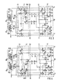
- the conventional parallel adder shown in FIG. 1 has four adder stages AS0, AS1, AS2 and AS3, which are intended to add a data word A0 A1 A2 A3 and a data word B0 B1 B2 B3.
- the indices 0, 1, 2 and 3 are assigned to the individual adder stages in ascending bit significance.
- each adding stage emits a sum signal on the one hand and a carry signal on the other.
- the sum signals of all four adder stages form the data word of the total sum calculated by the parallel adder.
- the output carry signal of each adder is fed to the subsequent adder so that each adder can process the carry of the previous adder.
- the adder AS0 responsible for the least significant digit is constantly entered the data value "0" as the carry signal.
- Each of the adder stages AS0 to AS3 is constructed in accordance with FIG. 2.
- This adding stage has two data inputs AE and BE, to which the data values to be added are fed.
- the sum calculated by this adding stage is available at the sum output SA.
- the adder stage receives the carry signal of the preceding adder stage via a transmission input CE and transmits its carry signal to the subsequent adder stage via a carry output CA.
- the adder stage has a summing circuit ST and a carry-out circuit CT. Both are connected between a positive pole + V and a negative pole -V of a voltage supply source.
- the carry-out circuit CT comprises a complementary stage CS, two coupling stages PKS, NKS and two switching transistors T5 and T6.
- the sum circuit ST forms the sum of the data input signals fed to the two data inputs AE and BE. This takes into account a carry forwarded via CE from a previous adding stage and a carry formed by CT from the input data signals. Since the present invention relates to the carry circuit CT, the structure and function of the summing circuit ST need not be discussed in detail here.
- the carry-out circuit CT comprises a complementary stage CS in the form of a series circuit connected to the positive pole + V with two P-channel transistors T7, T9 and a series circuit connected to the negative pole -V with two N-channel transistors T1, T3.
- the two series connections are connected to one another in a middle node K.
- the carry forming circuit CT further comprises a P-coupling circuit PKS and an N-coupling circuit NKS.
- the P-coupling circuit PKS has two P-channel transistors T8 and T10 connected in parallel, which are connected at one end to the positive pole + V and at the other end in a circuit node M1. The control electrodes of these two transistors are each connected to one of the two input data connections AE and BE.
- the N-coupling circuit NKS has a parallel connection of two N-channel transistors T2, T4, which are connected at one end to the negative pole -V and at the other end in a circuit node M2. The control electrodes of these transistors are each with one of the input data connections AE or BE connected.
- a series circuit comprising a P-channel transistor T6 and an N-channel transistor T5 is connected between the circuit nodes M1 and M2.
- the connection point is connected on the one hand to the center node K of the complementary stage CS and on the other hand both to the carry output connection CA and to the summing circuit ST.
- the control electrodes of T5 and T6 are connected to the transfer input terminal CE.
- the potential and thus the binary value of the output carry signal is determined by the potential of the center node K. If the binary value of the two input data signals is "0", the center node K is at a positive potential, so that the binary value "1" occurs at the output carry connection CA. If the binary value of the two input data signals is "1", negative potential arises via the center node K at the output carry connection CA. the binary value "0". The carry signal thus occurs in inverted form at the output carry terminal CA.
- the function of the switching transistors T5 and T6 is effective when the input signal data have different binary values. Then the series connection of T5 and T6 is at one end at the potential of + V and at the other end at the potential of -V. If an input carry signal with the binary value "0" is supplied via the input carry connection CE, T6 conducts while T5 blocks. Therefore, the potential at the output carry terminal CA assumes the potential of + V, thus has the binary value "1". Possessed the input carry signal, on the other hand, has the binary value "1", conducts T5, while T6 blocks. The binary value at the output carry port CA therefore becomes "0".
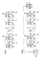
- Fig. 3 shows a P-type adding stage according to the invention. Like FIG. 2, this is basically designed in CMOS technology. Their summing circuit ST corresponds to that of FIG. 2. There is further agreement with regard to the complementary stage CS within the carry circuit CT.
- the carry circuit CT of FIG. 3 differs from the carry circuit CT of FIG. 2 in that it has only a P-coupling circuit PKS and a P-channel switching transistor T6, whereas the N-coupling circuit NKS and the N-channel switching transistor T5 are missing.
- each input data connection BE 'and AE' is assigned a presetting stage VSA or VSB.
- Each presetting stage comprises a series connection of 3 transistors T25, T26, T27 and T28, T29, T30, which is connected between the two poles + V and -V.
- the + V adjacent transistors are each P-channel transistors, while the remaining transistors of each presetting stage are N-channel transistors.
- the control electrode of one of the two N-channel transistors is connected to the input signal connection AE 'or BE'.
- the control electrodes of the other two transistors of each preset stage are connected to a preset terminal VA which is coupled to a preset signal source (not shown in FIG. 3).
- the connection point between the two transistors, the control electrodes of which are connected together to VA, is connected to the control electrodes of two transistors of the complementary stage CS.
- the input carry connection CE is connected to the control electrodes of P-channel transistors T19, T20 and the control electrodes of N-channel transistors T15, T16 of the summing circuit ST, in order to be able to take into account the carry delivered by the preceding adding stage when forming the sum.
- two inverters I1 and I2 are connected in this connection.
- the operation of the adder according to the invention is the same as in the known circuit with regard to the summing circuit ST, so that no further explanations are required here. Due to the differing carry-out circuit CT and the presetting stages VSA and VSB, the operation of the adding stage according to FIG. 3 explained below occurs.
- the binary value "1" is present at the presetting connections VA.
- the potential at the connection point BE '' between the transistors T25 and T26 and the potential at the connection point AE '' between the transistors T28 and T29 then depends on the respective binary value at the input data connections BE 'and AE'. If the connection points BE ′′ and AE ′′ have the same binary values, the circuit according to FIG. 3 behaves in exactly the same way as the known circuit according to FIG. 2. If both binary values are "0", the center node K and thus the output carry connection CA takes the binary value "1". If the binary values for AE '' and BE '' are both "1", the binary value "0" occurs at the output carry connection CA.
- the binary value "0" or the binary value "1” can occur at the input carry terminal CE and thus at the control electrode of the switching transistor T6, depending on the value of the carry supplied by the preceding adding stage. If the center node K is at a low potential corresponding to the binary value "0”, the switching transistor T6 is turned on when the binary value "0", that is to say a low potential, is supplied via the input carry terminal CE. T6 then switches the positive potential through from circuit node M1 to center node K, so that high potential corresponding to the binary value "1" occurs at the output carry terminal CA.
- the P-channel transistor T25 or T28 conducts and the N-channel transistor T26 or T29 blocks. This brings the potential of the positive pole + V to BE '' or AE '' via T25 or T28.
- the binary values available at the input data connections BE 'and AE' have no influence because T26 and T29 are blocked.
- the adding stage starts each computing phase with the switching state of the carry formation stage CS, from which the switching transistor T6 can be switched.
- N-type adder 4 shows an embodiment of an N-type adder. It largely coincides with the P-type adder shown in FIG. 3. The only difference is that instead of a P-coupling circuit there is an N-coupling circuit NKS, that the switching transistor T5 is an N-channel transistor and that between the presetting stages VSA and VSB and the switching points BE '' and AE '' respectively Inverter I1 or I2 is inserted.
- NKS N-coupling circuit
- the middle node K must be open during the presetting phase high potential value corresponding to the binary value "1" to ensure that the switching transistor T5 can be switched if this is necessary due to the binary value of the carry signal supplied.
- the presetting circuit has the effect that the carry formation circuit is brought into the state in which it could not be switched by the carry signal supplied. If, in the subsequent arithmetic phase, the carry signal supplied requires that the carry form circuit have this switching state, the switching state of the carry form circuit caused by the presetting is simply maintained. If, on the other hand, the carry signal supplied requires that the carry formation circuit is in the other switching state, a corresponding switchover is carried out.
- a parallel adder is preferably constructed so that adder stages of opposite types follow one another. This means that a P-type adder is followed by an N-type adder and this is in turn followed by a P-type adder.
- the advantage of this construction is that no inverter needs to be connected between the output carry connection and the input carry connection of the successive stages. This is because while the P-type adder requires the supply of the inverted input carry signal and outputs the non-inverted output carry signal at its output, the P-type adder requires the supply of the input carry signal in non-inverted form, while at its output carry connection it carries the carry signal in inverted form delivers.
- an additional improvement in the processing speed is achieved by coupling the input carry connection CE and the output carry connection CA of each adder via a load buffer device to the summing circuit ST of this adder.
- the load buffer device is formed by a series connection of two inverters I3 and I4. The load buffer device has the effect that the input capacitance of the switching transistor of the own and of the subsequent adder stage is not loaded more than necessary by the summing circuit.
- inverters I3 and I4 which are connected between the control terminal of the switching transistor T5 and the control terminals of the transistors T15, T16 and T19, T20 of the summing circuit ST, two further inverters 15 and 16 shown in broken lines Series connection is provided, which are connected between the center node K and the control terminals of the transistors T17 and T18 of the summing circuit ST.
- each adder stage has an output terminal Y connected to the output of the inverter I4 and an input terminal X connected to the control electrodes of the transistors T17 and T18 of the summing circuit ST.
- the input terminal X of an adder is connected to the output terminal Y of the subsequent adder.
- a parallel adder according to the invention with four adder stages is shown as an example in FIG. 5.
- adders AS0 and AS1 form a first group and adders AS2 and AS3 form a second group.
- the two adding stages are operated simultaneously in the presetting phase or the computing phase. While one group is in the presetting phase, the other group is operating in the computing phase.
- a buffer device ZS is provided, which temporarily stores the carry formed by the higher-order adder AS1 of the first group during its arithmetic phase and then transfers it to the lower-order adder AS2 when the group with the adders AS2 and AS3 from the presetting phase into the Calculation phase has passed. This prevents carryovers from being lost or faulty carryovers occurring during the phase switching of the two groups.
- Each of the two groups has a preset connection VA, to which the preset signal is fed, while the other group is in the computing phase.
- FIG. 6 A particularly preferred embodiment of a parallel adding unit according to the invention with four adding stages is shown as an example in FIG. 6.
- the output carry signal formed in the most significant adder AS3 is fed to an input CE of a carry feedback circuit CS2, which previously has an output CBQ by means of a preset signal applied to an input VA, into a no carry had brought characteristic condition.
- a carry selection circuit CS1 coupled to the carry feedback circuit CS2 is supplied with a preset signal at an input VA, the carry flag signal at an input CF and control signals at inputs ST1, ST2 and ST3.
- the control signals serve to select the carry signal to be fed to the input carry terminal CE of the least significant adder stage AS0.
- the buffer device is prepared in a separate presetting phase for the transfer of the carry. At the same time as the higher-order adding stages are switched to the presetting phase, the buffer device is also in its presetting phase. However, the presetting phase of the intermediate storage device ZS must be ended before the output carry signal, which has been calculated by the lower-order adder connected to it, is present at its input CE.
- an intermediate storage device is preferably constructed as shown in FIG. 8.
- a series connection of a P-channel transistor T40 and two N-channel transistors T41 and T42 is used, their P-channel transistor T40 connected to the positive pole + V and their N-channel connected to the negative pole -V -Transistor T42 are controlled jointly by the output of a pulse shaper stage IF, which is connected on the input side to a preset signal source device.
- the control electrode of the middle N-channel transistor T41 of the series circuit is on the one hand with the output of an N-channel transistor T39 controlled by an inverter stage I7 from the output of the pulse shaper stage IF and on the other hand via the output Y of an inverter stage I8 with the summing circuit ST of the preceding adder stage and a main electrode P-channel transistor T43 connected, the second main electrode of which is connected to the positive pole + V of the voltage supply source.
- the input carry terminal CE of the latch circuit ZE connected to the output carry terminal of the preceding adding stage is connected to the control electrode of the switching transistor T43.
- the output carry terminal CA of the latch circuit ZE is connected to the input carry terminal of the subsequent adding stage and forms a circuit node R with the connection between the P-channel transistor T40 and the middle N-channel transistor T41 of the series circuit.
- the buffer circuit ZS is preset, in that the pulse shaping circuit IF, after it has been started by the preset signal source device, sets its output to zero potential and thereby brings the circuit node R to a potential characterizing a binary "1" and via the inverter I7 and the output of the N-channel transistor T 39 and Inverter I8 also brings output Y to a binary "1".
- the buffer circuit is preset and remains in this state until it is switched by a signal which is present at the input CE and characterizes a carry.
- the zero potential pulse at the output of the pulse shaping circuit IF is terminated before the output carry signal calculated by the previous adding stage is present at the input CE of the buffer circuit ZS.
- the transistor T42 conducts, so that when the fast-switching P-channel transistor T43 is turned on by a binary "0", which denotes a carry, T41 also conducts, the output of which via the circuit node R is a binary, which denotes a carry "0" to the output CE of the latch circuit ZS.
- a logical "0" is now at the output Y via the inverter I8.
- the carry feedback circuit CS2 shown in FIGS. 7A and 7B, as well as the carry select circuit CS1, represent circuit parts of a preferred embodiment according to the invention. With their help, the output carry signal of the most significant adder is made available to the input carry connection of the least significant adder.
- the carry selection circuit CS1 shown in FIG. 7B offers the possibility of selecting which carry signal is to be fed to the input carry terminal by applying suitable control signals to the inputs ST1, ST2, ST3. So that in the event that the output carry signal is to be fed to the most significant adder, this can take place as quickly as the transfer of the calculated output carry signals from adder to adder, this part of the parallel adder must also be designed so that the carry output CBQ is preset.
- the carry feedback circuit CS2 shown in Figure 7A is constructed so that it has a series circuit of an N-channel transistor T33 and two P-channel transistors T31, T32, the N-channel transistor T33 and whose P-channel transistor T31, which is connected to the positive pole + V, is controlled jointly via the preparation connection VA by a preset signal source.
- the control electrode CE of the middle P-channel transistor T32 of the series circuit is supplied with the output carry signal of the most significant adder.
- Another series connection of a P-channel transistor T34 and an N-channel transistor T35 is between the positive pole + V and the negative Pol -V of the voltage supply source switched that the one main electrode of the P-channel transistor T34 is connected to the positive pole + V and its second main electrode with the one main electrode of the N-channel transistor T35 and the output CBQ of the carry-back circuit CS1 forms the circuit node S. .
- the control electrode of the P-channel transistor T34 is connected via an inverter I9 to the control electrode of the P-channel transistor T31 of the series circuit consisting of three transistors.
- the circuit node T formed by a main electrode of the P-channel transistor T32 and the N-channel transistor T33 with the control electrode of the N-channel transistor T35 is via an inverter I10 with the output X, which is the summing circuit ST of the most significant adder feeds the carry calculated in this stage.
- the embodiment of the carry selection circuit CS1 shown in FIG. 7B has a series connection of a P-channel transistor T36 connected to the positive pole + V and an N-channel transistor T 38 connected to the negative pole -V. With the connection point G of these transistors, a main electrode is connected to the N-channel transistor T37 which supplies the output carry signal to the most significant adder stage.
- the carry selection circuit CS1 has a selection logic AW, which evaluates the control signals fed to its inputs ST1, ST2, ST3 and the carry flag signal and the preset signal and selects the transistors T36, T37, T38 of the carry selection circuit CS1 via selection logic signals a, b, c so that each after the combination of the respective control signals, either the output carry signal CBQ supplied by the carry feedback circuit CS2 reaches the carry output CA of the carry select circuit CS1 via the transistor T37, or the transistors T36, T38 are controlled so that they put a constant binary "0" or "1” or the carry flag signal CF on the carry output CA.
- the carry selection circuit CS1 contains a pulse shaping circuit IS which is actuated by the preset signal and which makes the transistor briefly conductive via a NOR gate NOR1 with a "0" so as to preset the node G. This is necessary in case the carry comes from CBQ.
Landscapes
- Engineering & Computer Science (AREA)
- Physics & Mathematics (AREA)
- General Physics & Mathematics (AREA)
- Theoretical Computer Science (AREA)
- Pure & Applied Mathematics (AREA)
- Mathematical Analysis (AREA)
- Computational Mathematics (AREA)
- Computing Systems (AREA)
- Mathematical Optimization (AREA)
- General Engineering & Computer Science (AREA)
- Logic Circuits (AREA)
- Manipulation Of Pulses (AREA)
- Electronic Switches (AREA)
Priority Applications (5)
| Application Number | Priority Date | Filing Date | Title |
|---|---|---|---|
| EP90107878A EP0453600B1 (fr) | 1990-04-25 | 1990-04-25 | Additionneur parallèle |
| DE59010655T DE59010655D1 (de) | 1990-04-25 | 1990-04-25 | Paralleladdierwerk |
| US07/688,187 US5128892A (en) | 1990-04-25 | 1991-04-19 | Parallel adder |
| KR1019910006484A KR100235146B1 (ko) | 1990-04-25 | 1991-04-23 | 병렬 가산기 |
| JP3095333A JPH04251330A (ja) | 1990-04-25 | 1991-04-25 | 並列加算器 |
Applications Claiming Priority (1)
| Application Number | Priority Date | Filing Date | Title |
|---|---|---|---|
| EP90107878A EP0453600B1 (fr) | 1990-04-25 | 1990-04-25 | Additionneur parallèle |
Publications (2)
| Publication Number | Publication Date |
|---|---|
| EP0453600A1 true EP0453600A1 (fr) | 1991-10-30 |
| EP0453600B1 EP0453600B1 (fr) | 1997-02-26 |
Family
ID=8203912
Family Applications (1)
| Application Number | Title | Priority Date | Filing Date |
|---|---|---|---|
| EP90107878A Expired - Lifetime EP0453600B1 (fr) | 1990-04-25 | 1990-04-25 | Additionneur parallèle |
Country Status (5)
| Country | Link |
|---|---|
| US (1) | US5128892A (fr) |
| EP (1) | EP0453600B1 (fr) |
| JP (1) | JPH04251330A (fr) |
| KR (1) | KR100235146B1 (fr) |
| DE (1) | DE59010655D1 (fr) |
Cited By (1)
| Publication number | Priority date | Publication date | Assignee | Title |
|---|---|---|---|---|
| EP0744687A1 (fr) * | 1995-05-24 | 1996-11-27 | STMicroelectronics S.A. | Circuit logique combinatoire |
Families Citing this family (6)
| Publication number | Priority date | Publication date | Assignee | Title |
|---|---|---|---|---|
| JP2530070B2 (ja) * | 1991-09-11 | 1996-09-04 | 株式会社東芝 | 加算器 |
| US5406506A (en) * | 1993-11-09 | 1995-04-11 | United Microelectronics Corp. | Domino adder circuit having MOS transistors in the carry evaluating paths |
| WO1996030853A1 (fr) * | 1995-03-31 | 1996-10-03 | Tadashi Shibata | Circuit arithmetique a semi-conducteur |
| US5706420A (en) * | 1995-06-06 | 1998-01-06 | Hewlett-Packard Company | Super pipelined speculative execution vector generator |
| US6134576A (en) * | 1998-04-30 | 2000-10-17 | Mentor Graphics Corporation | Parallel adder with independent odd and even sum bit generation cells |
| KR100297721B1 (ko) * | 1998-10-29 | 2001-08-07 | 윤종용 | 반도체 장치간 신호 송수신을 위한 송신회로 및 수신회로 |
Citations (2)
| Publication number | Priority date | Publication date | Assignee | Title |
|---|---|---|---|---|
| DE3540800A1 (de) * | 1985-11-16 | 1987-08-13 | Standard Elektrik Lorenz Ag | Binaeraddierer-zelle und aus solchen binaeraddierer-zellen zusammengesetztes schnelles addier- und multiplizierwerk |
| US4910700A (en) * | 1988-06-10 | 1990-03-20 | General Electric Company | Bit-sliced digit-serial multiplier |
Family Cites Families (5)
| Publication number | Priority date | Publication date | Assignee | Title |
|---|---|---|---|---|
| JPS5810241A (ja) * | 1981-07-10 | 1983-01-20 | Toshiba Corp | 加算器 |
| US4471454A (en) * | 1981-10-27 | 1984-09-11 | Ibm Corporation | Fast, efficient, small adder |
| IT1210751B (it) * | 1987-05-20 | 1989-09-20 | Cselt Centro Studi Lab Telecom | Sommatore veloce in tecnologia c mos |
| US4885716A (en) * | 1988-08-15 | 1989-12-05 | Dallas Semiconductor Corporation | High speed carry chain |
| US5010509A (en) * | 1988-10-05 | 1991-04-23 | United Technologies Corporation | Accumulator for complex numbers |
-
1990
- 1990-04-25 EP EP90107878A patent/EP0453600B1/fr not_active Expired - Lifetime
- 1990-04-25 DE DE59010655T patent/DE59010655D1/de not_active Expired - Fee Related
-
1991
- 1991-04-19 US US07/688,187 patent/US5128892A/en not_active Expired - Lifetime
- 1991-04-23 KR KR1019910006484A patent/KR100235146B1/ko not_active Expired - Fee Related
- 1991-04-25 JP JP3095333A patent/JPH04251330A/ja active Pending
Patent Citations (2)
| Publication number | Priority date | Publication date | Assignee | Title |
|---|---|---|---|---|
| DE3540800A1 (de) * | 1985-11-16 | 1987-08-13 | Standard Elektrik Lorenz Ag | Binaeraddierer-zelle und aus solchen binaeraddierer-zellen zusammengesetztes schnelles addier- und multiplizierwerk |
| US4910700A (en) * | 1988-06-10 | 1990-03-20 | General Electric Company | Bit-sliced digit-serial multiplier |
Non-Patent Citations (3)
| Title |
|---|
| IEEE INTERNATIONAL ELECTRON DEVICES MEETING, TECHNICAL DIGEST, Washington, 6. - 8. Dezember 1976, Seiten 21-26, IEEE, New York, US; R.A. ALLEN et al.: "Charge coupled devices in digital LSI" * |
| PATENT ABSTRACTS OF JAPAN, Band 7, Nr. 82 (P-189)[1227], 6. April 1983; & JP-A-58 10 241 (TOKYO SHIBAURA DENKI K.K.) 20-01-1983 * |
| PROCEEDINGS OF THE IEEE 1986 CUSTOM INTEGRATED CIRCUITS CONFERENCE, Rochester, New York, 12. - 15. Mai 1986, Seiten 236-239, IEEE, New York, US; C.M. LEE et al.: "Zipper CMOS" * |
Cited By (2)
| Publication number | Priority date | Publication date | Assignee | Title |
|---|---|---|---|---|
| EP0744687A1 (fr) * | 1995-05-24 | 1996-11-27 | STMicroelectronics S.A. | Circuit logique combinatoire |
| FR2734675A1 (fr) * | 1995-05-24 | 1996-11-29 | Sgs Thomson Microelectronics | Circuit logique combinatoire |
Also Published As
| Publication number | Publication date |
|---|---|
| EP0453600B1 (fr) | 1997-02-26 |
| US5128892A (en) | 1992-07-07 |
| DE59010655D1 (de) | 1997-04-03 |
| JPH04251330A (ja) | 1992-09-07 |
| KR100235146B1 (ko) | 1999-12-15 |
| KR910018900A (ko) | 1991-11-30 |
Similar Documents
| Publication | Publication Date | Title |
|---|---|---|
| DE3413139A1 (de) | Programmierte logikanordnung mit einer hilfshochzieheinrichtung zur erhoehung der vorlaufladegeschwindigkeit | |
| DE4115081A1 (de) | Logikschaltung fuer asynchrone schaltungen mit n-kanal-logikblock und dazu inversem p-kanal-logikblock | |
| DE2510604C2 (de) | Integrierte Digitalschaltung | |
| DE3940897C2 (de) | Schaltungsanordnung und Verfahren zur Berechnung digitaler Summen in einem Halbleiteraddierer mit Parallelübertrag | |
| DE2656086C2 (de) | Rechenanlage | |
| EP0453600B1 (fr) | Additionneur parallèle | |
| DE1125208B (de) | Elektrisches Vergleichsschaltungssystem | |
| DE3526521C2 (fr) | ||
| EP0224656B1 (fr) | Additionneur à propagation de retenue à plusieurs étages en technique CMOS avec deux types de cellules d'addition | |
| EP0208275A2 (fr) | Dispositif d'addition parallèle par bit de nombres binaires | |
| DE1287128B (de) | Logische Schaltung mit mehreren Stromlenkgattern | |
| DE1537307A1 (de) | Logische Schaltung | |
| DE2000275A1 (de) | Elektronischer Walzenschalter | |
| DE69026363T2 (de) | Multipositionsverschieber mit Paritätsbitgenerator | |
| DE2334744A1 (de) | Binaer-logikschaltung fuer digitale rechenoperationen | |
| DE2304007A1 (de) | Asynchron-schaltkreis | |
| EP0218071B1 (fr) | Cellule d'addition pour un additionneur à propagation de retenue en technique CMOS | |
| DE2948340A1 (de) | Informationsuebertragungssystem | |
| EP0905892A2 (fr) | Bascule RS avec des entrées de validation | |
| DE1549446A1 (de) | Digitalrechner | |
| DE1094020B (de) | Periodisch arbeitende numerische Rechenmaschine | |
| DE2336143A1 (de) | Logische schaltung | |
| DE102022127143B4 (de) | Bereichssegmentierung für analogen cam-speicher mit verbesserter genauigkeit | |
| EP0333884A1 (fr) | Circuit multiplieur parallèle-série ainsi que ses étages de multiplication et d'addition | |
| DE2332431A1 (de) | Flip-flop |
Legal Events
| Date | Code | Title | Description |
|---|---|---|---|
| PUAI | Public reference made under article 153(3) epc to a published international application that has entered the european phase |
Free format text: ORIGINAL CODE: 0009012 |
|
| AK | Designated contracting states |
Kind code of ref document: A1 Designated state(s): DE FR GB IT NL |
|
| 17P | Request for examination filed |
Effective date: 19920305 |
|
| GRAG | Despatch of communication of intention to grant |
Free format text: ORIGINAL CODE: EPIDOS AGRA |
|
| 17Q | First examination report despatched |
Effective date: 19960523 |
|
| GRAH | Despatch of communication of intention to grant a patent |
Free format text: ORIGINAL CODE: EPIDOS IGRA |
|
| GRAH | Despatch of communication of intention to grant a patent |
Free format text: ORIGINAL CODE: EPIDOS IGRA |
|
| GRAA | (expected) grant |
Free format text: ORIGINAL CODE: 0009210 |
|
| AK | Designated contracting states |
Kind code of ref document: B1 Designated state(s): DE FR GB IT NL |
|
| ITF | It: translation for a ep patent filed | ||
| ET | Fr: translation filed | ||
| GBT | Gb: translation of ep patent filed (gb section 77(6)(a)/1977) |
Effective date: 19970312 |
|
| REF | Corresponds to: |
Ref document number: 59010655 Country of ref document: DE Date of ref document: 19970403 |
|
| PLBE | No opposition filed within time limit |
Free format text: ORIGINAL CODE: 0009261 |
|
| STAA | Information on the status of an ep patent application or granted ep patent |
Free format text: STATUS: NO OPPOSITION FILED WITHIN TIME LIMIT |
|
| 26N | No opposition filed | ||
| REG | Reference to a national code |
Ref country code: GB Ref legal event code: IF02 |
|
| PGFP | Annual fee paid to national office [announced via postgrant information from national office to epo] |
Ref country code: GB Payment date: 20020417 Year of fee payment: 13 |
|
| PGFP | Annual fee paid to national office [announced via postgrant information from national office to epo] |
Ref country code: NL Payment date: 20030403 Year of fee payment: 14 |
|
| PGFP | Annual fee paid to national office [announced via postgrant information from national office to epo] |
Ref country code: FR Payment date: 20030418 Year of fee payment: 14 |
|
| PG25 | Lapsed in a contracting state [announced via postgrant information from national office to epo] |
Ref country code: GB Free format text: LAPSE BECAUSE OF NON-PAYMENT OF DUE FEES Effective date: 20030425 |
|
| GBPC | Gb: european patent ceased through non-payment of renewal fee | ||
| PG25 | Lapsed in a contracting state [announced via postgrant information from national office to epo] |
Ref country code: NL Free format text: LAPSE BECAUSE OF NON-PAYMENT OF DUE FEES Effective date: 20041101 |
|
| PG25 | Lapsed in a contracting state [announced via postgrant information from national office to epo] |
Ref country code: FR Free format text: LAPSE BECAUSE OF NON-PAYMENT OF DUE FEES Effective date: 20041231 |
|
| NLV4 | Nl: lapsed or anulled due to non-payment of the annual fee |
Effective date: 20041101 |
|
| REG | Reference to a national code |
Ref country code: FR Ref legal event code: ST |
|
| PG25 | Lapsed in a contracting state [announced via postgrant information from national office to epo] |
Ref country code: IT Free format text: LAPSE BECAUSE OF NON-PAYMENT OF DUE FEES;WARNING: LAPSES OF ITALIAN PATENTS WITH EFFECTIVE DATE BEFORE 2007 MAY HAVE OCCURRED AT ANY TIME BEFORE 2007. THE CORRECT EFFECTIVE DATE MAY BE DIFFERENT FROM THE ONE RECORDED. Effective date: 20050425 |
|
| PGFP | Annual fee paid to national office [announced via postgrant information from national office to epo] |
Ref country code: DE Payment date: 20050531 Year of fee payment: 16 |
|
| PG25 | Lapsed in a contracting state [announced via postgrant information from national office to epo] |
Ref country code: DE Free format text: LAPSE BECAUSE OF NON-PAYMENT OF DUE FEES Effective date: 20061101 |