EP0453612A1 - Leuchtdiodenmatrix - Google Patents
Leuchtdiodenmatrix Download PDFInfo
- Publication number
- EP0453612A1 EP0453612A1 EP90108112A EP90108112A EP0453612A1 EP 0453612 A1 EP0453612 A1 EP 0453612A1 EP 90108112 A EP90108112 A EP 90108112A EP 90108112 A EP90108112 A EP 90108112A EP 0453612 A1 EP0453612 A1 EP 0453612A1
- Authority
- EP
- European Patent Office
- Prior art keywords
- layer
- semiconductor
- light emitting
- top surface
- emitting diode
- Prior art date
- Legal status (The legal status is an assumption and is not a legal conclusion. Google has not performed a legal analysis and makes no representation as to the accuracy of the status listed.)
- Withdrawn
Links
Images





Classifications
-
- H—ELECTRICITY
- H10—SEMICONDUCTOR DEVICES; ELECTRIC SOLID-STATE DEVICES NOT OTHERWISE PROVIDED FOR
- H10H—INORGANIC LIGHT-EMITTING SEMICONDUCTOR DEVICES HAVING POTENTIAL BARRIERS
- H10H29/00—Integrated devices, or assemblies of multiple devices, comprising at least one light-emitting semiconductor element covered by group H10H20/00
- H10H29/10—Integrated devices comprising at least one light-emitting semiconductor component covered by group H10H20/00
- H10H29/14—Integrated devices comprising at least one light-emitting semiconductor component covered by group H10H20/00 comprising multiple light-emitting semiconductor components
-
- B—PERFORMING OPERATIONS; TRANSPORTING
- B41—PRINTING; LINING MACHINES; TYPEWRITERS; STAMPS
- B41J—TYPEWRITERS; SELECTIVE PRINTING MECHANISMS, i.e. MECHANISMS PRINTING OTHERWISE THAN FROM A FORME; CORRECTION OF TYPOGRAPHICAL ERRORS
- B41J2/00—Typewriters or selective printing mechanisms characterised by the printing or marking process for which they are designed
- B41J2/435—Typewriters or selective printing mechanisms characterised by the printing or marking process for which they are designed characterised by selective application of radiation to a printing material or impression-transfer material
- B41J2/447—Typewriters or selective printing mechanisms characterised by the printing or marking process for which they are designed characterised by selective application of radiation to a printing material or impression-transfer material using arrays of radiation sources
- B41J2/45—Typewriters or selective printing mechanisms characterised by the printing or marking process for which they are designed characterised by selective application of radiation to a printing material or impression-transfer material using arrays of radiation sources using light-emitting diode [LED] or laser arrays
Definitions
- the present invention relates to a light emitting diode (LED) array employable in an electronic printer for photography, and particularly to an improvement of light emitting windows in the LED array.
- LED light emitting diode
- Fig. 1 illustrates the structure of a conventional LED array 1.
- the LED array 1 comprises a semiconductor body 10 having an N-GaAs layer 3, an N-Al x Ga 1-x As layer 4 and P-Al x Ga 1-x As regions 5.
- An N-electrode layer 2 is formed on the bottom surface of the semiconductor body 10, while an insulating layer 8 is provided on the top surface of the semiconductor body 10.
- the insulating layer 8 has a linear array of rectangular windows 9, which are defined on the P-regions 5.
- P-electrode layers 11 are formed on the insulating layer 8 and respective end portions thereof are in contact with the top surfaces of the P-regions 5 through the windows 9.
- Fig. 2 is a schematic diagram showing the situation in which the LED array 1 is employed in an electronic printer for photography.
- the LED array 1 is fixed to a base plate 21 such as a printed board, and the electric connection between the LED array 1 and the base plate 21 is attained through die bonding and wire bonding.
- a self-focus lens array (SLA) 22 is supported by a supporting member (not shown) so that the windows 9 (Fig. 1) face to the SLA 22 across a gap therebetween.
- a photosensitive drum 23 is rotatably provided and the center axis of the drum 23 is located on a line passing through the LED array 1 and the SLA 22.
- An image signal is transmitted to an LED drive circuit (not shown), and in response to the image signal, the LED drive circuit selectively supplies electric power to the LEDs included in the LED array 1 through the electrodes 2 and 11.
- the LEDs supplied with the electric power generate light L1 at the PN junctions thereof and emit the light L1 through the windows 9.
- the SLA 22 converts the light L1 into converging light L2, which is applied to the photosensitive surface 24 of the drum 23.
- the SLA 22 is effective for preventing the light spot from spreading on the photosensitive surface 24 of the drum 23.
- the photosensitive surface 24 of the drum 23 Prior to the exposure to the light L2, the photosensitive surface 24 of the drum 23 is electrostatically charged to a negative level.
- the photosensitive surface 24 When the light L2 is applied to the photosensitive surface 24, only the part of the surface 24 exposed to the light L2 is discharged. Therefore, a latent image is obtained on the photosensitive surface 24 by repeating the light generating process while rotating the drum 23 around the axis thereof. Then, the photosensitive surface 24 is supplied with toner charged to a negative level, and the toner stays only on the discharged part of the surface 24 since the toner cannot stay on the non-discharged part due to electrostatic repulsive force. The toner staying on the surface 24 are transferred onto a paper, and then, the image thus obtained is fixed by heat and pressure.
- the transmission efficiency of light is about several percent in the LED array head consisting of the LED array 1, the base plate 21, the SLA 22 and a driver (not shown). This is because the SLA 22, which has a relatively low transmission efficiency of light, should be provided in the conventional LED array head. Therefore, it has been desired to provide an LED array which can be used at a high transmission efficiency of light.
- a light emitting diode array comprises: (a) a semiconductor layer of a first conductivity type: (b) semiconductor regions of a second conductivity type which are selectively formed in a top surface of the semiconductor layer; (c) a first electrode layer formed on a bottom surface of the semiconductor layer: (d) second electrode layers provided on respective first areas in top surfaces of the semiconductor regions; and (e) an opaque layer provided on the semiconductor regions and having through holes which communicate with second areas in the top srufaces of the semiconductor regions, respectively.
- the light emitting diode array further comprises: (f) an insulating layer provided on the top surface of the semiconductor layer and having windows on the semiconductor regions, respectively.
- the present invention is also directed to a method of fabricating a light emitting diode array.
- the method comprises the steps of: (a) preparing a semiconductor wafer having a semiconductor layer of a first conductivity type therein; (b) forming a matrix array of semiconductor regions of a second conductivity type in a top surface of the semiconductor layer; (c) forming an insulating layer on the top surface of the semiconductor layer; (d) selectively removing the insulating layer to obtain windows on the semiconductor regions; (e) forming a conductive layer on the insulating layer and in the windows; (f) selectively removing the conductive layer to obtain first electrode layers having first portions being in contact with first areas in top surfaces of the semiconductor layers and second portions located on the insulating layer, respectively; (g) forming a opaque layer on the insulating layer, on the first electrode layers and in the windows; (h) selectively removing the opaque layer to obtain through holes in the opaque layer on the semiconductor regions, respectively; (i) forming a second electrode
- an object of the present invention is to provide an LED array usable at a high transmission efficiency of light.
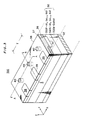
- the LED array 100 comprises a semiconductor body 30 having an N-GaAs buffer layer 33 on which an N-Al x Ga 1-x As layer 34 is formed.
- a linear array of P-Al x Ga 1-x As regions or wells 35 is formed along the direction X, as also shown in Fig. 4A, which is a secitonal view of the LED array 100 along line A-A.
- the respective boundaries between the P-layers 35 and the N-Al x Ga 1-x As layer 34 are PN junctions 41, which are also aligned in the direction X.
- An N-electrode layer 32 is formed on the bottom surface of the semiconductor body 30.
- an insulating layer 36 having windows 37 is formed on the top surface of the semiconductor body 30, an insulating layer 36 having windows 37 is formed.
- the windows 37 are provided on the P-layers 35, respectively, and a linear array of P-electrode layers 39 is formed along the array of windows 37.
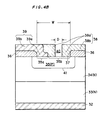
- Fig. 4B there is shown an enlarged cross section of the LED array 100 along line B-B in Fig. 3.
- Each of the P-electrode layers 39 has a first portion 39a being in contact with an area 35a on the corresponding P-region 35 and a second portion 39b provided on the insulating layer 36.
- an opaque layer 38 is provided on the semicondctor body 30.
- the opaque layer 38 is made of silicon oxide in which black dye is mixed, and has a first portion 38a filling the window 37 (except for a hole 40 which is described later) and a second portion 38b covering the insulating layer 36.
- the first portion 38a is in contract with another area 35b on the P-region 35.
- the top surface of the opaque layer 38 is aligned with respective top surfaces of the electrode portions 39b and is in parallel to the X-Y plane.
- Respective windows 37 have a common size W, and the diameter D of each through hole 40 is smaller than the size W of the windows 37.
- the diameter D is smaller than a half (W/2) of the size W and, in the preferred embodiment shown in Figs. 3, 4A and 4B, the diameter D is about a quarter of the window size W.
- the diameter D defines the diameter of photobeams emitted from the LED array 100. Accordingly, the diameter D may be determined in accordance with the diameter of photobeams which is required in an apparatus in which the LED array 100 is employed.
- the through holes are circular holes and extend in the vertical direction Z.
- Fig. 5 is a schematic side view of an electronic printer for photography in which the LED array 100 is employed.
- the LED array 100 is mounted on a base plate 21 such as a printed board through die bond and wiring bond.
- the device thus obtained is so oriented that the openings of the through holes 40 face to the photosensitive surface 24 of a rotatable photosensitive drum 23.
- the LED cells in the LED array 100 selectively generate light at the PN junctions 41 (Fig. 3).
- the light is selectively blocked by the opaque layer 38 and is emitted through the holes 40 in the form of parallel photobeams L3.
- the photosensitive surface 24 which is previously charged is selectively exposed to the photobeams L3.
- a latent image which is obtained on the photosensitive surface 24 by repeating the light-emission process while rotating the drum 23 is transferred to a paper through the same process with the conventional printer.
- each of the photobeams L3 has a small diameter corresponding to the diameter D of the holes 40, an SLA is not required in the LED array head shown in Fig.5. As a result, the transmission efficiency of light is improved as compared with the conventional LED array head.
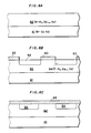
- the LED array 100 may be fabricated as follows: First, as shown in Fig. 6A, an N-GaAs substrate or wafer 61 is prepared, and an N-Al x Ga 1-x As layer 62 is formed thereon through an expitaxial growth process. Then, a mask layer is formed on the top surface of the layer 62 and is selectively removed through a photolithography process, whereby a mask pattern 63 (Fig. 6B) having a matrix array of windows is obtained. While using the mask pattern 63 as an implantation mask, P-type impurity ions are selectively implanted in the top surface of the layer 62 to thereby obtain a matrix array of P-Al x Ga 1-x As regions or wells 64.
- an insulating layer 65 made of silicon oxide is formed on the top surface of the layers 62 and 64. Then, the insulating layer 65 is removed through a photolithography process to obtain windows 66 (Fig, 6D) on the P-regions 64. An aluminum paste is applied to the whole top surface, and by hardening the same, an aluminum layer 67 (Fig. 6E) is obtained.
- the aluminum layer 67 is selectively removed to obtain aluminum bridges 67a (Fig. 6F) each of which is in contact with two of the P-regions 64 adjacent to each other in the direction Y.
- the removal of the aluminum layer 67 is an alternate removal in the direcrion Y, and therefore, the aluminum bridges 67a cover every second portion of the insulating layer 65 in the direction Y.
- the aluminum bridge 67a is located on the portion 65b of the insulating layer 65, but there are no aluminum bridges on the portions 65a and 65c.
- the P-regions 64 are arrayed in a matrix form on the top surface of the N-layer 62, a number of portions each corresponding to the portion are aligned in the direction X perpendicular to the drawing sheet and the aluminum bridges 67a are also aligned in the direction X.
- an opaque layer 68 (Fig. 6G) made of silicon oxide and black dye is formed on the respective top surfaces.
- the top part of the opaque layer 68 is removed through an etching process so that the top surface of the opaque layer 68 is shaped into a plane aligned with the respective top surfaces of the aluminum bridges 67a (Fig. 6H).
- Through holes 40 communicating with the P-regions 64 are formed through a photolithography process and an aluminum layer 69 is formed on the bottom surface of the N-layer 61.
- the wafer shown in Fig. 6H is then cut into strips along lines LN with a dicing machine, where each of the strips extends in the direction X and has a linear array of LED cells.
- Each strip thus obtained corresponds to the LED array 100 shown in Figs. 3, 4A and 4B, where the correspondence between respective layers are shown in Fig. 6H by reference numerals in parenthesis.
- the layer 69 may be formed before the fabrication of the top structure is completed.
- the opaque layer 38 may be a black glass layer which is coated on the top surface. The present invention can be also applied to a single LED cell having the structure in the section T shown in Fig. 3.
- the LED array according to the present invention can be used at a high transmission efficiency of light since the same requires no SLA. In other words, a required intensity of light can be obtained even from a relatively low electric power and the cost in fabricating an LED array head and that in driving the same are decreased.
Landscapes
- Physics & Mathematics (AREA)
- Optics & Photonics (AREA)
- Health & Medical Sciences (AREA)
- General Health & Medical Sciences (AREA)
- Toxicology (AREA)
- Led Devices (AREA)
- Printers Or Recording Devices Using Electromagnetic And Radiation Means (AREA)
- Dot-Matrix Printers And Others (AREA)
Priority Applications (4)
| Application Number | Priority Date | Filing Date | Title |
|---|---|---|---|
| JP63279387A JPH02126687A (ja) | 1988-11-07 | 1988-11-07 | Ledアレイ |
| US07/513,848 US5038186A (en) | 1988-11-07 | 1990-04-24 | Light emitting diode array |
| CA002015358A CA2015358C (en) | 1988-11-07 | 1990-04-25 | Light emitting diode array |
| EP90108112A EP0453612A1 (de) | 1988-11-07 | 1990-04-27 | Leuchtdiodenmatrix |
Applications Claiming Priority (3)
| Application Number | Priority Date | Filing Date | Title |
|---|---|---|---|
| JP63279387A JPH02126687A (ja) | 1988-11-07 | 1988-11-07 | Ledアレイ |
| CA002015358A CA2015358C (en) | 1988-11-07 | 1990-04-25 | Light emitting diode array |
| EP90108112A EP0453612A1 (de) | 1988-11-07 | 1990-04-27 | Leuchtdiodenmatrix |
Publications (1)
| Publication Number | Publication Date |
|---|---|
| EP0453612A1 true EP0453612A1 (de) | 1991-10-30 |
Family
ID=27168740
Family Applications (1)
| Application Number | Title | Priority Date | Filing Date |
|---|---|---|---|
| EP90108112A Withdrawn EP0453612A1 (de) | 1988-11-07 | 1990-04-27 | Leuchtdiodenmatrix |
Country Status (4)
| Country | Link |
|---|---|
| US (1) | US5038186A (de) |
| EP (1) | EP0453612A1 (de) |
| JP (1) | JPH02126687A (de) |
| CA (1) | CA2015358C (de) |
Cited By (2)
| Publication number | Priority date | Publication date | Assignee | Title |
|---|---|---|---|---|
| EP0519226A3 (en) * | 1991-05-21 | 1993-02-24 | Mitsubishi Denki Kabushiki Kaisha | Led array head type electrophotographic recording apparatus |
| EP0718720A1 (de) * | 1994-12-19 | 1996-06-26 | Xerox Corporation | Drucksystem |
Families Citing this family (4)
| Publication number | Priority date | Publication date | Assignee | Title |
|---|---|---|---|---|
| JPH0480072U (de) * | 1990-11-27 | 1992-07-13 | ||
| JPH04243170A (ja) * | 1991-01-17 | 1992-08-31 | Eastman Kodak Japan Kk | 発光ダイオード |
| US5591680A (en) * | 1993-12-06 | 1997-01-07 | Micron Communications | Formation methods of opaque or translucent films |
| JP2001102626A (ja) * | 1999-07-28 | 2001-04-13 | Canon Inc | Ledチップ、ledアレイチップ、ledアレイヘッド及び画像形成装置 |
Citations (2)
| Publication number | Priority date | Publication date | Assignee | Title |
|---|---|---|---|---|
| FR2406861A1 (fr) * | 1977-10-19 | 1979-05-18 | Radiotechnique Compelec | Perfectionnement aux dispositifs de visualisation comportant une mosaique de diodes electroluminescentes |
| DE3541790A1 (de) * | 1984-11-26 | 1986-07-03 | Hitachi Cable, Ltd., Tokio/Tokyo | Lichtemittierende festkoerper-diodenanordnung |
Family Cites Families (8)
| Publication number | Priority date | Publication date | Assignee | Title |
|---|---|---|---|---|
| JPS58223382A (ja) * | 1982-06-21 | 1983-12-24 | Toshiba Corp | 半導体発光装置 |
| JPS6037575A (ja) * | 1983-08-10 | 1985-02-26 | Sanyo Electric Co Ltd | プリンタの光学系調整方法 |
| JPS6140068A (ja) * | 1984-07-31 | 1986-02-26 | Sanyo Electric Co Ltd | 光プリンタ用発光ダイオ−ド |
| JPS6195956A (ja) * | 1984-10-18 | 1986-05-14 | Matsushita Electric Ind Co Ltd | 電子写真記録装置 |
| JPS61207086A (ja) * | 1985-03-11 | 1986-09-13 | Oki Electric Ind Co Ltd | 発光素子アレイ |
| NL8600675A (nl) * | 1986-03-17 | 1987-10-16 | Philips Nv | Halfgeleiderinrichting voor het opwekken van een elektronenstroom. |
| JPS6356967A (ja) * | 1986-08-28 | 1988-03-11 | Nec Corp | 発光ダイオ−ド |
| JPH01128480A (ja) * | 1987-11-13 | 1989-05-22 | Oki Electric Ind Co Ltd | 発光ダイオードアレイ |
-
1988
- 1988-11-07 JP JP63279387A patent/JPH02126687A/ja active Pending
-
1990
- 1990-04-24 US US07/513,848 patent/US5038186A/en not_active Expired - Fee Related
- 1990-04-25 CA CA002015358A patent/CA2015358C/en not_active Expired - Fee Related
- 1990-04-27 EP EP90108112A patent/EP0453612A1/de not_active Withdrawn
Patent Citations (2)
| Publication number | Priority date | Publication date | Assignee | Title |
|---|---|---|---|---|
| FR2406861A1 (fr) * | 1977-10-19 | 1979-05-18 | Radiotechnique Compelec | Perfectionnement aux dispositifs de visualisation comportant une mosaique de diodes electroluminescentes |
| DE3541790A1 (de) * | 1984-11-26 | 1986-07-03 | Hitachi Cable, Ltd., Tokio/Tokyo | Lichtemittierende festkoerper-diodenanordnung |
Non-Patent Citations (1)
| Title |
|---|
| PATENT ABSTRACTS OF JAPAN, vol. 11, no. 41 (E-478)[2488], 6th February 1987; & JP-A-61 207 086 (OKI ELECTRIC IND. CO., LTD) 13-09-1986 * |
Cited By (2)
| Publication number | Priority date | Publication date | Assignee | Title |
|---|---|---|---|---|
| EP0519226A3 (en) * | 1991-05-21 | 1993-02-24 | Mitsubishi Denki Kabushiki Kaisha | Led array head type electrophotographic recording apparatus |
| EP0718720A1 (de) * | 1994-12-19 | 1996-06-26 | Xerox Corporation | Drucksystem |
Also Published As
| Publication number | Publication date |
|---|---|
| JPH02126687A (ja) | 1990-05-15 |
| US5038186A (en) | 1991-08-06 |
| CA2015358C (en) | 1994-08-23 |
Similar Documents
| Publication | Publication Date | Title |
|---|---|---|
| US5045895A (en) | Light emitting diode array with electrodes | |
| US6180960B1 (en) | Surface light-emitting element and self-scanning type light-emitting device | |
| EP2610910B1 (de) | Anordnung von lichtemittierenden Dioden und Druckkopf | |
| KR100954051B1 (ko) | 발광 소자 어레이 및 화상형성장치 | |
| EP0779661B1 (de) | LED-Anordnung mit hoher Auflösung und ihr Herstellungsverfahren | |
| US20070262333A1 (en) | Light-emitting element array and image forming apparatus | |
| US6781246B2 (en) | Semiconductor array device with single interconnection layer | |
| US5038186A (en) | Light emitting diode array | |
| US5094970A (en) | Method of making a light emitting diode array | |
| US7259397B2 (en) | Self-scanning light-emitting element array chip | |
| JPH111027A (ja) | Ledアレイおよびプリントヘッドならびに電子写真プリンタ | |
| JP2006179862A (ja) | 発光ダイオードアレイパッケージ構造およびその方法 | |
| CA2015462C (en) | Light emitting diode array | |
| EP1115162A1 (de) | An der kante licht emitierende anordnung mit verbesserter externer leucht-effizienz und deren verwendung in einer selbst abtastenden leuchtdioden-anordnung | |
| EP0214674B1 (de) | Verfahren zum Justieren der Lichtausstrahlung einer Leuchtdiode bei einem vorgegebenen Treibstrom | |
| JP4511273B2 (ja) | 光プリンタヘッド、その製造方法及び光プリンタ | |
| JPH0985985A (ja) | 光プリントヘッドおよびロッドレンズ・ユニット | |
| JP3184063B2 (ja) | 受発光方法、受発光素子およびその製造方法 | |
| JP3315196B2 (ja) | Ledプリントヘッド | |
| JP3256128B2 (ja) | 受発光ダイオードアレイチップおよび該チップを用いた受発光ダイオードアレイ、該チップの製造方法 | |
| JPH0568869B2 (de) | ||
| JPH06310755A (ja) | Ledアレイチップおよびその製造方法 | |
| JPH02305482A (ja) | 半導体光電変換装置 | |
| JPS60187070A (ja) | 半導体発光装置 | |
| JPH02125766A (ja) | Ledアレイ |
Legal Events
| Date | Code | Title | Description |
|---|---|---|---|
| PUAI | Public reference made under article 153(3) epc to a published international application that has entered the european phase |
Free format text: ORIGINAL CODE: 0009012 |
|
| 17P | Request for examination filed |
Effective date: 19901212 |
|
| AK | Designated contracting states |
Kind code of ref document: A1 Designated state(s): DE GB IT |
|
| 17Q | First examination report despatched |
Effective date: 19940207 |
|
| STAA | Information on the status of an ep patent application or granted ep patent |
Free format text: STATUS: THE APPLICATION IS DEEMED TO BE WITHDRAWN |
|
| 18D | Application deemed to be withdrawn |
Effective date: 19940818 |