EP0453693B1 - Pockelseffekt-Messsonde für elektrische Felder - Google Patents
Pockelseffekt-Messsonde für elektrische Felder Download PDFInfo
- Publication number
- EP0453693B1 EP0453693B1 EP90403751A EP90403751A EP0453693B1 EP 0453693 B1 EP0453693 B1 EP 0453693B1 EP 90403751 A EP90403751 A EP 90403751A EP 90403751 A EP90403751 A EP 90403751A EP 0453693 B1 EP0453693 B1 EP 0453693B1
- Authority
- EP
- European Patent Office
- Prior art keywords
- crystal
- sensor according
- polarization
- incident beam
- electric field
- Prior art date
- Legal status (The legal status is an assumption and is not a legal conclusion. Google has not performed a legal analysis and makes no representation as to the accuracy of the status listed.)
- Expired - Lifetime
Links
- 230000005684 electric field Effects 0.000 title claims description 59
- 230000005697 Pockels effect Effects 0.000 title claims description 12
- 239000013078 crystal Substances 0.000 claims description 151
- 230000010287 polarization Effects 0.000 claims description 49
- 239000000835 fiber Substances 0.000 claims description 29
- 238000004458 analytical method Methods 0.000 claims description 27
- 239000013307 optical fiber Substances 0.000 claims description 20
- 230000003287 optical effect Effects 0.000 claims description 16
- 230000002457 bidirectional effect Effects 0.000 claims description 4
- 238000001514 detection method Methods 0.000 claims description 4
- 230000014759 maintenance of location Effects 0.000 claims 2
- 238000005259 measurement Methods 0.000 description 57
- 239000000523 sample Substances 0.000 description 42
- 230000005672 electromagnetic field Effects 0.000 description 6
- 238000012423 maintenance Methods 0.000 description 5
- 230000004044 response Effects 0.000 description 5
- PEDCQBHIVMGVHV-UHFFFAOYSA-N Glycerine Chemical compound OCC(O)CO PEDCQBHIVMGVHV-UHFFFAOYSA-N 0.000 description 4
- 230000008901 benefit Effects 0.000 description 4
- 230000005540 biological transmission Effects 0.000 description 3
- 238000010586 diagram Methods 0.000 description 3
- 239000013598 vector Substances 0.000 description 3
- VYPSYNLAJGMNEJ-UHFFFAOYSA-N Silicium dioxide Chemical compound O=[Si]=O VYPSYNLAJGMNEJ-UHFFFAOYSA-N 0.000 description 2
- 229910052797 bismuth Inorganic materials 0.000 description 2
- JCXGWMGPZLAOME-UHFFFAOYSA-N bismuth atom Chemical compound [Bi] JCXGWMGPZLAOME-UHFFFAOYSA-N 0.000 description 2
- 230000008859 change Effects 0.000 description 2
- 230000028161 membrane depolarization Effects 0.000 description 2
- 238000000034 method Methods 0.000 description 2
- 230000010363 phase shift Effects 0.000 description 2
- 230000009467 reduction Effects 0.000 description 2
- 238000004026 adhesive bonding Methods 0.000 description 1
- 230000008878 coupling Effects 0.000 description 1
- 238000010168 coupling process Methods 0.000 description 1
- 238000005859 coupling reaction Methods 0.000 description 1
- 230000000694 effects Effects 0.000 description 1
- 230000006698 induction Effects 0.000 description 1
- 238000002347 injection Methods 0.000 description 1
- 239000007924 injection Substances 0.000 description 1
- 229910052500 inorganic mineral Inorganic materials 0.000 description 1
- 229910052751 metal Inorganic materials 0.000 description 1
- 239000002184 metal Substances 0.000 description 1
- 239000011707 mineral Substances 0.000 description 1
- 230000007935 neutral effect Effects 0.000 description 1
- 230000005693 optoelectronics Effects 0.000 description 1
- 230000000750 progressive effect Effects 0.000 description 1
- 230000001902 propagating effect Effects 0.000 description 1
- 230000010349 pulsation Effects 0.000 description 1
- 239000000377 silicon dioxide Substances 0.000 description 1
Images


Classifications
-
- G—PHYSICS
- G01—MEASURING; TESTING
- G01D—MEASURING NOT SPECIALLY ADAPTED FOR A SPECIFIC VARIABLE; ARRANGEMENTS FOR MEASURING TWO OR MORE VARIABLES NOT COVERED IN A SINGLE OTHER SUBCLASS; TARIFF METERING APPARATUS; MEASURING OR TESTING NOT OTHERWISE PROVIDED FOR
- G01D5/00—Mechanical means for transferring the output of a sensing member; Means for converting the output of a sensing member to another variable where the form or nature of the sensing member does not constrain the means for converting; Transducers not specially adapted for a specific variable
- G01D5/26—Mechanical means for transferring the output of a sensing member; Means for converting the output of a sensing member to another variable where the form or nature of the sensing member does not constrain the means for converting; Transducers not specially adapted for a specific variable characterised by optical transfer means, i.e. using infrared, visible, or ultraviolet light
- G01D5/32—Mechanical means for transferring the output of a sensing member; Means for converting the output of a sensing member to another variable where the form or nature of the sensing member does not constrain the means for converting; Transducers not specially adapted for a specific variable characterised by optical transfer means, i.e. using infrared, visible, or ultraviolet light with attenuation or whole or partial obturation of beams of light
- G01D5/34—Mechanical means for transferring the output of a sensing member; Means for converting the output of a sensing member to another variable where the form or nature of the sensing member does not constrain the means for converting; Transducers not specially adapted for a specific variable characterised by optical transfer means, i.e. using infrared, visible, or ultraviolet light with attenuation or whole or partial obturation of beams of light the beams of light being detected by photocells
- G01D5/344—Mechanical means for transferring the output of a sensing member; Means for converting the output of a sensing member to another variable where the form or nature of the sensing member does not constrain the means for converting; Transducers not specially adapted for a specific variable characterised by optical transfer means, i.e. using infrared, visible, or ultraviolet light with attenuation or whole or partial obturation of beams of light the beams of light being detected by photocells using polarisation
-
- G—PHYSICS
- G01—MEASURING; TESTING
- G01R—MEASURING ELECTRIC VARIABLES; MEASURING MAGNETIC VARIABLES
- G01R1/00—Details of instruments or arrangements of the types included in groups G01R5/00 - G01R13/00 and G01R31/00
- G01R1/02—General constructional details
- G01R1/06—Measuring leads; Measuring probes
- G01R1/067—Measuring probes
- G01R1/07—Non contact-making probes
- G01R1/071—Non contact-making probes containing electro-optic elements
-
- G—PHYSICS
- G01—MEASURING; TESTING
- G01R—MEASURING ELECTRIC VARIABLES; MEASURING MAGNETIC VARIABLES
- G01R15/00—Details of measuring arrangements of the types provided for in groups G01R17/00 - G01R29/00, G01R33/00 - G01R33/26 or G01R35/00
- G01R15/14—Adaptations providing voltage or current isolation, e.g. for high-voltage or high-current networks
- G01R15/24—Adaptations providing voltage or current isolation, e.g. for high-voltage or high-current networks using light-modulating devices
- G01R15/241—Adaptations providing voltage or current isolation, e.g. for high-voltage or high-current networks using light-modulating devices using electro-optical modulators, e.g. electro-absorption
- G01R15/242—Adaptations providing voltage or current isolation, e.g. for high-voltage or high-current networks using light-modulating devices using electro-optical modulators, e.g. electro-absorption based on the Pockels effect, i.e. linear electro-optic effect
-
- G—PHYSICS
- G01—MEASURING; TESTING
- G01R—MEASURING ELECTRIC VARIABLES; MEASURING MAGNETIC VARIABLES
- G01R29/00—Arrangements for measuring or indicating electric quantities not covered by groups G01R19/00 - G01R27/00
- G01R29/08—Measuring electromagnetic field characteristics
- G01R29/0864—Measuring electromagnetic field characteristics characterised by constructional or functional features
- G01R29/0878—Sensors; antennas; probes; detectors
- G01R29/0885—Sensors; antennas; probes; detectors using optical probes, e.g. electro-optical, luminescent, glow discharge, or optical interferometers
-
- G—PHYSICS
- G01—MEASURING; TESTING
- G01R—MEASURING ELECTRIC VARIABLES; MEASURING MAGNETIC VARIABLES
- G01R29/00—Arrangements for measuring or indicating electric quantities not covered by groups G01R19/00 - G01R27/00
- G01R29/12—Measuring electrostatic fields or voltage-potential
-
- G—PHYSICS
- G02—OPTICS
- G02F—OPTICAL DEVICES OR ARRANGEMENTS FOR THE CONTROL OF LIGHT BY MODIFICATION OF THE OPTICAL PROPERTIES OF THE MEDIA OF THE ELEMENTS INVOLVED THEREIN; NON-LINEAR OPTICS; FREQUENCY-CHANGING OF LIGHT; OPTICAL LOGIC ELEMENTS; OPTICAL ANALOGUE/DIGITAL CONVERTERS
- G02F1/00—Devices or arrangements for the control of the intensity, colour, phase, polarisation or direction of light arriving from an independent light source, e.g. switching, gating or modulating; Non-linear optics
- G02F1/01—Devices or arrangements for the control of the intensity, colour, phase, polarisation or direction of light arriving from an independent light source, e.g. switching, gating or modulating; Non-linear optics for the control of the intensity, phase, polarisation or colour
- G02F1/03—Devices or arrangements for the control of the intensity, colour, phase, polarisation or direction of light arriving from an independent light source, e.g. switching, gating or modulating; Non-linear optics for the control of the intensity, phase, polarisation or colour based on ceramics or electro-optical crystals, e.g. exhibiting Pockels effect or Kerr effect
Definitions
- the subject of the present invention is a Pockels effect electric field sensor comprising as a sensitive element a crystalline body having electro-optical properties, crossed by an incident light beam, with determined directions of propagation and polarization. It allows to measure not only the value of an electric field but also its direction.
- the refractive indices which generally depend on the direction of propagation and the polarization of the incident beam, vary linearly with an applied external electric field. This is the Pockels effect, known since the end of the last century. This variation in index can be used to change the phase of the light beam; this can then be measured by an interferometric system as this is done in electro-optical modulators.
- the tensor of the Pockels effect generally includes 18 non-zero rij coefficients (with 1 ⁇ i ⁇ 6 and 1 ⁇ j ⁇ 3) and the same phase variation can be obtained for several orientations and several electric field values.
- These sensors use optical fibers to guide the incident beam entering the crystal and to guide the beam leaving the latter.
- the polarization of the incident beam is carried out by polarizers placed just before the crystal and the analysis of the beam leaving the crystal is carried out with an analyzer placed just after the crystal.
- These polarizers and analyzers are located in the measurement probe, which has the disadvantage of increasing the dimensions of the latter and therefore of preventing the measurement of electric field in confined spaces.
- the crystal operates in transmission, which prohibits performing electric field measurements near a wall.
- the electro-optical crystals used have a dielectric constant greater than 10 (16 in the case of bismuth germanate Bi 4 Ge 3 O 12 ). Also, such a crystal of any shape can induce distortions in the electric field lines, which means that such sensors give a good order of magnitude of the electric field measured, but that the real value and the direction of this field provided by these sensors are in no way guaranteed. These sensors are therefore not reliable.
- the probe crystals used are cut in the shape of cubes and therefore have a very strong vibrational resonance in their response to their natural frequency of vibration, equal to c / 2a where c is the speed of sound in the crystal and has the side of the cube.
- this natural frequency is around 400 kHz and induces significant disturbances in the studies of electric shocks.
- Tanaka recommends using, as a sensitive element with Pockels effect, a component of parallelepiped shape comprising on two opposite sides, perpendicular to the electric field to be measured, dielectric layers whose dielectric constant has an intermediate value between that of the sensitive element and that of the ambient medium, allowing a more progressive variation of the constant dielectric.
- the subject of the invention is precisely an electric field sensor with a Pockels effect which makes it possible to remedy the various drawbacks mentioned above.
- this sensor allows a precise measurement of the value of the electric field and a precise determination of the orientation of this field.
- this sensor can ensure an electric field measurement near a wall and the probe part of this sensor can be made with smaller dimensions than those of the probes of the prior art.
- the influence of the resonance frequencies of the crystal is very significantly reduced.
- the invention relates to an electric field sensor with Pockels effect comprising as sensitive element a crystal with electro-optical properties, crossed by a light beam with determined directions of propagation and polarization, characterized in that the crystal is cut in the form of an ellipsoid and has a crystallographic symmetry either uniaxial 622, 422 or 4 ⁇ 2m, or cubic 4 ⁇ 3m or 23, the three perpendicular axes of the ellipsoid being oriented along three crystallographic axes trirectangles of highest symmetry of the crystal, the crystal further having at least a couple of diametrically opposite and parallel flats and arranged at the place where l 'one of the three-directional crystallographic axes emerges from the crystal.
- the axes of the ellipsoid must be parallel to the axis of order 6 and to a pair of axes of order 2 perpendicular to each other.
- a crystal probe cut according to the invention in the form of an ellipsoid and in particular in the form of a sphere makes it possible to eliminate the geometric distortions of the electric field to be measured produced by the crystal.
- the originality of the invention lies in the simultaneous conjunction of the following two properties of the probe: macroscopic, ellipsoidal shape and particular cubic or uniaxial crystallographic symmetry of the crystal.
- the first property makes it possible to ensure the constancy of the electric field in the probe and to link in a one-to-one way its value with that of the preexisting field before the introduction of the probe; the second allows one-to-one link the electro-optical effects measured to the field prevailing in the probe.
- the crystals to which the invention applies are those for which the electro-optical tensor (or de Pockels) has only three non-zero coefficients r41, r52, r63 (the first index indicates the line of the tensor and the second indicates the column).
- these three coefficients are equal while they are different for crystals of uniaxial symmetry 622, 422 and 4 ⁇ 2m.
- the optical response of the sensor for a crystal with cubic symmetry will be identical for the three perpendicular components of the electric field whereas it will be different for a crystal with uniaxial symmetry. In the latter case, these components can be calculated from the knowledge of the coefficients r41, r52 and r63 as determined by previous work or by prior calibration in a uniform electric field of known value and direction.
- the component of the electric field can be precisely measured in a direction determined by the user, regardless of the orientation of the electric field.
- the sensor of the invention can therefore be a single-channel sensor.
- the single-channel version can only be obtained for certain orientations of the axes of the ellipsoid relative to the crystallographic axes, which is not the case for a spherical sensor.
- the sensor of the invention advantageously comprises three optical measurement channels allowing the three perpendicular components of the electric field to be measured independently.
- the parts of the measurement channels situated in the crystal are oriented respectively along the three trirectangular crystallographic axes of the latter's highest symmetry.
- each measurement channel comprises a monochromatic light source emitting an incident beam, a means for polarizing the incident beam in a first crystallographic direction of the crystal, means for introducing the beam incident polarizes in the crystal in a second crystallographic direction, a means for analyzing the light beam leaving the crystal and an element for detecting the analyzed light signal.
- the crystal comprises at least two pairs of flat areas parallel to the places where said crystallographic axes emerge from the crystal.
- each measurement channel comprises an input optical fiber with polarization maintenance for transporting the incident beam and an output optical fiber with polarization maintenance for the transport of the beam leaving the crystal.
- This type of fiber makes it possible to place the polarization means directly at the output of the light source and the analysis means directly at the input of the detection element. This allows a significant reduction in the probe part of the sensor compared to that of the prior art, which is made according to the invention of the crystal alone.
- polarization-maintaining fibers makes it possible to distance the polarization and analysis means from the crystal and therefore to reduce the disturbance of the lines of the electric field to be measured.
- the crystal works in reflection.
- the incident beam entering the crystal and the beam leaving this crystal form an angle of at most 5 °.
- the amplitude of the light wave transported by the output optical fiber varies linearly with the electric field to be measured.
- the light intensity detected by the detector varies quadratically with the electric field.
- the direction of polarization of the incident beam and the direction of analysis of the beam leaving the crystal, for each measurement channel are parallel.
- the same optical fiber can be used for each measurement channel, alternately ensuring the transport of the incident beam and the transport of the beam leaving the crystal.
- a single focusing lens disposed opposite the polarization and analysis element, with an axis perpendicular to the flats of the crystal, can alternately ensure the collimation of the incident beam from the fiber and then focusing the beam leaving the crystal in this same fiber.
- the polarization and the analysis being carried out in the vicinity of the probe crystal it is possible to use instead of monomode fibers with polarization maintenance, for each measurement channel, a multimode fiber (for example of 125 micrometers of outside diameter with a core of 50 micrometers) for which the coupling problems are much less critical (the core of a single-mode fiber with polarization maintenance has dimensions of approximately 7 micrometers).
- a multimode fiber for example of 125 micrometers of outside diameter with a core of 50 micrometers
- the core of a single-mode fiber with polarization maintenance has dimensions of approximately 7 micrometers.
- FIG. 1 The block diagram of the sensor of the invention shown in Figure 1 shows a single sensor measurement path for measuring a single component of an electric field. For a sensor with three measurement channels, these channels are similar.
- Each measurement channel comprises a light source 2 constituted by a single-mode laser diode emitting a monochromatic light beam 4.
- This beam 4 is polarized rectilinearly in a first direction x or y by a polarizer 6 then focuses in a single-mode input fiber 8 to polarization maintenance by a focusing lens 10 of the Selfoc lens type of "pitch" 0.25.
- the axis of polarization of the fiber 8 is oriented in the first direction.
- a collimating lens 12 of the Selfoc lens type of "pitch" 0.25 used to collimate the polarized incident beam before it enters the probe crystal 14 via a first flat 16.
- the incident beam collimated entering the probe crystal bears the reference 17.
- the probe crystal is an electro-optical monocrystal of uniaxial symmetry 622, 422 or 4 ⁇ 2m, or cubic symmetry 4 ⁇ 3m (such as Bi 4 Ge 3 O 12 ) or 23 cut in the form of an ellipsoid or a sphere.
- the incident beam 17 which penetrates into the crystal 14 through the flat 16 is then reflected on a second flat 18 of the crystal to emerge through the flat 16.
- the flat 16 and 18 are diametrically opposite and constitute a pair of flat. They are polished according to an optical quality and placed at the place where one of the three three-directional crystallographic axes (100), (010) or (001) of the crystal emerges from the sphere 14.
- the injection of the incident beam 17 into the crystal takes place in a second direction z perpendicular to the first direction of polarization x or y.
- the incident beam 17 entering through the flat 16 in the probe crystal and the beam 20 leaving the crystal through this flat 16 form an angle between them at most equal to 5 °.
- the beam 20 leaving the crystal 14 is focused using a focusing lens 24 also of the Selfoc lens type of "pitch" 0.25 in a second polarization maintaining fiber 26 which is parallel to the input fiber 8 and located on the same side of the probe crystal 14.
- the axis of polarization of the output fiber is perpendicular to that of the input fiber 8 and perpendicular to the direction of propagation of the light beam; if the first direction is the direction x, the axis of polarization of the fiber 26 is oriented in the direction y and if the first direction is the direction y, the axis of polarization of the fiber 26 is oriented in the direction x.
- the directions x, y and z are parallel to three trirectangular axes of the highest symmetry of the crystal.
- the collimated measurement beam 29 is then received by an analyzer 30 crossed at 90 ° relative to the polarizer 6, then detected by a detector 32 of the photodiode type.
- the lenses 10 and 12 are bonded to the two ends of the fiber 8 and the lenses 24 and 28 are bonded to the two ends of the fiber 26.
- the lenses 12 and 24 are bonded directly to the sphere 14 opposite the flat 16.
- the operating principle of the sensor is the measurement of the ellipticity induced in the crystal by the electric field to be measured. This measurement is carried out by comparing the phase difference between the polarizations of the incident beam 17 and the measurement beam 20. It only makes sense if this phase measurement is possible over the entire section of the beams (since the detector measures the total power of these beams). This implies inter alia that the light path is the same for all light rays, that is to say that the beams propagate in a plane wave inside the crystal. Even if the light path is the same for all the rays outside the crystal, the condition of propagation in plane wave in the crystal can only be achieved, taking into account the finite transverse dimension of the beams, if the diopter 16 by which penetrates the incident beam is plane.
- FIGS 2a and 2b illustrate the operating principle of the sensor of the invention.
- the sphere of the indices 31 becomes an ellipsoid 33 whose main axes are the axes (110), ( 1 ⁇ 10) and (001) respectively denoted X, Y, Z (FIG. 2b).
- Figure 2a shows the ellipticity created in the xy plane in the presence of a field Ee ⁇ according to z and FIG. 2b is a section of the ellipsoid of the indices 33 in the xy plane.
- the electric field of the incident polarized beam remains in the XY plane and is only sensitive to the index variations induced in this plane by the continuous field.
- Ei ⁇ / 2 and dn Y -r.no 3 .
- the ellipticity created is therefore directly proportional to the value of the field Ee ⁇ .
- the beam 20 emerging from the probe crystal 14 comes out with an elliptical polarization in the xy plane perpendicular to the direction z of propagation since the axes XY of the ellipsoid of the indices 33 are the bisectors of the angle xy.
- This elliptical polarization is easily detected by the analyzer 30 oriented perpendicular to the directions of propagation and polarization of the incident beam 17, that is to say along the direction (010) or y.
- the emerging beam 20 remains polarized in the xz plane, defined by the incident wave vector and the polarizer, which is a main plane of the crystal.
- This xz plane being perpendicular to the yz plane which is the other main plane of the analyzer crystal, no signal is detected.
- the sensor of the invention makes it possible to measure not only the value of the electric field but also its direction.
- ⁇ e is the relative dielectric constant of the ambient medium, generally close to unity (case of air) and ⁇ i is the dielectric constant of the probe crystal. So the field Ei ⁇ in the crystal is directly connected by a simple proportionality factor to the field Ee ⁇ . to measure.
- the reflection of the incident beam 17 on the flat 18 is possible because the refractive index of the mineral electro-optical crystals is relatively high (2 in the case of Bi 4 Ge 3 O 12 ).
- the loss of light intensity due to the reflection factor less than 1 is partially compensated by the doubling of the ellipticity due to the doubling of the optical path in the probe crystal.
- n (l) are the depolarization coefficients, and are numbers which depend on the shape of the ellipsoid.
- the block diagram in Figure 1 showed a single optical measurement channel.
- FIG. 3 shows an embodiment of the sensor of the invention comprising three optical channels at the level of the probe crystal 14 respectively 40, 42 and 44. Each measurement channel is sensitive only to the component of the field electric parallel to the propagation of the incident light beam 17 (or emerging from the sensor 20).
- the measurement channel 40 is sensitive to the component (001) of the electric field
- the measurement channel 42 is sensitive to the component of the electric field in the direction (010)
- the optical channel 44 is sensitive to the component of the field electric oriented in direction (100).
- the probe crystal 14 comprises three pairs of flats 16a-18a, 16b-18b and 16c-18c respectively, optically polished, the flats 18a, 18b and 18c being diametrically opposite the flats 16a, 16b and 16c.
- the pairs of flats 16a-18a, 16b-18b and 16c-18c are arranged respectively at the places where the crystallographic axes (001), (010) and (100) emerge from the crystal.
- the flats 16a, 16b and 16c are used for the entry and exit of the incident beams disturbed by the crystal; the flats 18a, 18b and 18c ensure the reflection of the incident beams in the crystal.
- FIG. 3 the directions of polarization P and of analysis A of the incident beams 17 and outgoing 20 are indicated, corresponding to the orientation of the axes of polarization of the input and output fibers and therefore to that of the component of the electric field to be detected.
- the polarizer is oriented in the direction (100) and the analyzer is oriented in the direction (010); for the measurement channel 42, the polarizer is oriented in the direction (001) and the analyzer in a direction (100); for measurement channel 44 the polarizer is oriented in the direction (001) and the analyzer in a direction (010).
- the directions of polarization and analysis can be swapped.
- the sensor shown has only two pairs of flat areas 16A-18A and 16B-18B respectively diametrically opposite, oriented respectively along the crystallographic planes (110) and ( 1 ⁇ 10) of the probe crystal 14, but always three optical measurement channels 46, 48 and 50 respectively, parts of which located in the crystal are oriented along the crystallographic axes of the crystal. These three channels 46, 48 and 50 are used to independently measure the three components of the electric field E1, E2 and E3 respectively.
- the propagation direction ( 1 ⁇ 10) of the incident beams 17 and emerging 20 is used to measure the components E1 and E2 of the electric field parallel to the directions (110) and (001).
- two pairs of polarizers and analyzers P46-A46 and P48-A48 are used oriented at 45 ° to one another for the measurement channels 46 and 48 which are parallel.
- the P46 polarizers and P48 form an angle of 45 ° between them and the analyzers A46 and A48 form an angle of 45 ° between them, the polarizer P46 and analyzer A46 being crossed at 90 ° and the polarizer P48 and analyzer A48 being also crossed at 90 °.
- This configuration is represented in FIG. 5, in the plane of the flat 16 (crystallographic plane ( 1 ⁇ 10)).
- the third component E3 of the electric field oriented in the direction ( 1 ⁇ 10) is measured by propagating the incident beam in the direction (110) using the measurement channel 50.
- the advantage of this embodiment is to place as many optical fibers as possible on the same side of the probe so as to be able to easily carry out measurements in places difficult to access.
- the measurement channels 46 and 48 are parallel.
- the crystal was placed, for each measurement channel, between an analyzer A and a polarizer P crossed at 90 ° oriented at 45 ° to the main axes of the ellipsoid of the indices 33.
- the positions respective of the polarizer P and the analyzer A are shown in FIG. 2b.
- Polarizer P was oriented in one direction (( X ⁇ - Y ⁇ ) / 2 and the analyzer A was perpendicular to the polarizer P and therefore oriented in the direction (( X ⁇ + Y ⁇ ) / 2 .
- the quarter wave plate 34 has been inserted, the neutral lines of which are 45 ° from the polarization axes of the polarizer and of the analyzer and therefore parallel to the axes of the ellipsoid.
- this blade induces a phase shift of ⁇ ⁇ / 2 between the components parallel to X and Y.
- Em1 Ew 2 X ⁇ - Y ⁇ E represents the amplitude of the initial electromagnetic field and w represents its pulsation.
- the probe crystal acquires an induced birefringence which creates a phase advance ⁇ of the component of the electromagnetic field parallel to X ⁇ and a phase delay - ⁇ of the component of the electromagnetic field parallel to Y ⁇ equal to ( ⁇ / ⁇ ) r.no 3 . Ei ⁇ .
- Em2 Ew 2 (e i ⁇ X ⁇ -e -i ⁇ Y ⁇ )
- Em3 Ew 2 (e i ( ⁇ + ⁇ ⁇ / 2) X ⁇ -e -i ⁇ Y ⁇ )
- the quarter-wave plate can be positioned either before or after the probe crystal, or even be split into two eighth wave plates, one being placed before the crystal and the other after .
- the amplitude of the electromagnetic field Em4 after the analyzer is equal to the scalar product P.Em3, where P represents the polarization vector, that is:
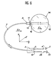
- Each measurement channel comprises a light source 2 constituted by a laser diode, single mode or multimode, emitting a monochromatic light beam 4 intended to be conveyed by a multimode optical fiber 7 made of silica of the type 50 ⁇ m of core diameter and 125 ⁇ m of external diameter.
- This optical fiber 7 is equipped, at a first end, with a bidirectional coupler 3 comprising a branch 5 placed opposite the laser diode 2 so as to recover the incident beam 4.
- the multimode optical fiber is also used for transporting the light beam leaving the probe crystal 14 which is an ellipsoid of xyz axes or more particularly a sphere of Bi 4 Ge 3 O 12 .
- the bidirectional coupler 3 has a branch 15 placed opposite the detector 32 of the photodiode type, used to direct the analysis measurement beam 29 onto the detector 32.
- the end of the optical fiber 7 opposite to that equipped with the bidirectional coupler 3 is equipped with a lens 9 of the Selfoc lens type of "Pitch" (or “fractional pitch") 0.25 alternately serving to collimate the incident beam 4 before its entry into the probe crystal 14, via the first flat 16 of the crystal, then to focus the light beam leaving the probe crystal 14, still via the flat 16, in the multimode optical fiber 7.
- a lens 9 of the Selfoc lens type of "Pitch" (or “fractional pitch") 0.25 alternately serving to collimate the incident beam 4 before its entry into the probe crystal 14, via the first flat 16 of the crystal, then to focus the light beam leaving the probe crystal 14, still via the flat 16, in the multimode optical fiber 7.
- the polarization of the incident beam and the analysis of the beam leaving the probe crystal 14 are ensured by the same element 11 consisting of a polarizing film bonded to the face of the lens 9 opposite to that mounted at the end of the fiber.
- This polarizing film 11 is for example a sheet of the polaroid type about 0.5 mm thick.
- the linearization of the output signal is obtained by a single plate 13, an eighth wave inserted between the polarizing film 11 and the probe sphere 14.
- This plate 13 can be held facing the flat 16 by gluing at its periphery on the flat. .
- the incident beam 4 carried by the optical fiber 7 is first of all collimated by the lens 9 and polarized by the polarizing film 11 in the direction x or y perpendicular to the direction z of propagation of the field crystal electric Ee ⁇ to measure.
- the collimated and polarized beam penetrates into the probe crystal 14 via the flat 16 to be reflected on the flat 18, diametrically opposite, then comes out through the flat 16.
- the beam leaving the crystal 14 in turn crosses the plate 13, then the polarizing element 11, then serving as an analyzer, to be focused by the lens 9 in the optical fiber 7 and to be directed by the coupler 3 on the photodiode 32 to be detected.
- the sensor shown in FIG. 6 can be a sensor with three pairs of flats, or else a sensor with two couples of flats as described above.
- the parallelism of the direction of polarization of the incident beam and of the direction of analysis of the beam leaving the crystal, for an optical path for measuring an electric field by Pockels effect is not limited to a cut crystal. in the form of an ellipsoid and in particular of a sphere.
- This characteristic applies to any crystal having two opposite parallel faces, at the points of entry and exit of the light beam, in particular two planar faces. This characteristic takes all its interest when an original arrangement is implemented, namely the operation in reflection, since it makes it possible to use a single fiber to guide the incident beam and the outgoing beam.
Landscapes
- Physics & Mathematics (AREA)
- General Physics & Mathematics (AREA)
- Nonlinear Science (AREA)
- Chemical & Material Sciences (AREA)
- Engineering & Computer Science (AREA)
- Ceramic Engineering (AREA)
- Crystallography & Structural Chemistry (AREA)
- Optics & Photonics (AREA)
- Electromagnetism (AREA)
- Measuring Instrument Details And Bridges, And Automatic Balancing Devices (AREA)
- Investigating Or Analysing Materials By Optical Means (AREA)
Claims (19)
- Pockelseffekt-Meßsonde, als empfindliches Element einen Kristall (14) mit elektrooptischen Eigenschaften umfassend, durchquert von einem Lichtbündel (17, 20) von bestimmter Ausbreitungs- und Polarisationsrichtung,
dadurch gekennzeichnet,
daß der Kristall in Form eines Ellipsoids geschliffen ist und eine kristallographische Symmetrie aufweist, entweder einachsig 622, 422 oder

- Sonde nach Anspruch 1, dadurch gekennzeichnet, daß der Kristall kugelförmig geschliffen ist.
- Sonde nach einem der Ansprüche 1 oder 2, dadurch gekennzeichnet, daß sie wenigstens eine Meßstrecke enthält, umfassend eine ein eintreffendes Bündel (4) ausstrahlende monochromatische Lichtquelle (2), eine Einrichtung (6) zum Polarisieren des einfallenden Bündels entsprechend einer ersten kristallographischen Richtung des Kristalls (14), Einleiteinrichtungen (9, 12) des polarisierten eintreffenden Bündels (17) in den Kristall entsprechend einer zweiten kristallographischen Richtung, eine Analyseeinrichtung (30) des aus dem Kristall austretenden Lichtbündels (20) und ein Detektionselement (32) des analysierten Lichtsignals.
- Sonde nach einem der Ansprüche 1 bis 3, dadurch gekennzeichnet, daß drei optische Meßstrecken (40-42-44; 46-48-50) umfaßt, um die drei senkrechten Komponenten des elektrischen Feldes unabhängig zu messen, wobei die in dem Kristall befindlichen Teile dieser Meßstrecken entsprechend den drei, drei rechte Winkel bildenden, kristallographischen Achsen der größten Symmetrie des Kristalls orientiert sind.
- Sonde nach einem der Ansprüche 1 bis 4, dadurch gekennzeichnet, daß der Kristall wenigstens zwei Paare von parallelen, paarweise diametral entgegengesetzten Flächen bzw. Anflachungen (16a-18a, 16b-18b, 16c-18c, 16A-18A, 16B-18B) an den Stellen aufweist, wo die kristallographischen Achsen aus dem Kristall austreten.
- Sonde nach einem der Ansprüche 1 bis 5, dadurch gekennzeichnet, daß es ein Kristall der Symmetrie 43 m ist, insbesondere aus Bi4Ge3O12.
- Sonde nach Anspruch 6, dadurch gekennzeichnet, daß die Polarisationseinrichtung (6) jeder Meßstrecke sich direkt am Ausgang der Lichtquelle (2) befindet, und dadurch, daß die Analyseeinrichtung (30) sich direkt am Eingang des Detektionselements (32) befindet, und dadurch, daß jede Meßstrecke außerdem eine optische Eingangsfaser (8) mit Polarisationsaufrechterhaltung für die Übertragung des eintreffenden Bündels umfaßt und eine optische Ausgangsfaser (26) mit Polarisationsaufrechterhaltung für die Übertragung des aus dem Kristall austretenden Bündels.
- Sonde nach Anspruch 7, dadurch gekennzeichnet, daß jede Meßstrecke außerdem umfaßt: eine erste Fokussierlinse (10), angeordnet am Ausgang der Polarisationseinrichtung (6), um das eintreffende Bündel in die Eingangsfaser (8) zu fokussieren, eine erste Kollimationslinse (12), angeordnet am Ausgang der Eingangsfaser (8), um das eintreffende, in den Kristall eindringende Bündel (17) zu sammeln, eine zweite Fokussierlinse (24), angeordnet am Ausgang des Kristalls, um das aus dem Kristall austretende Bündel (20) in die Ausgangsfaser (26) zu fokussieren, und eine zweite Kollimationslinse, angeordnet am Ausgang der Ausgangsfaser (26), um das aus dem Kristall austretende Bündel auf die Analyseeinrichtung (30) zu fokussieren.
- Sonde nach Anspruch 8, dadurch gekennzeichnet, daß die erste Kollimationslinse (12) und die zweite Fokussierlinse (24) auf derselben Seite des Kristalls (14) angeordnet sind.
- Sonde nach einem der Ansprüche 3 bis 9, dadurch gekennzeichnet, daß bei jeder Meßstrecke der eintreffende, in den Kristall eindringende Strahl (17) und der aus dem Kristall austretende Strahl (20) einen Winkel von höchstens 5° bilden.
- Sonde nach Anspruch 10, dadurch gekennzeichnet, daß die optischen Eingangs- und Ausgangs fasern von zwei Meßstrecken (46, 48) auf auf ein und derselben Seite des Kristalls angeordnet sind.
- Sonde nach einem der Ansprüche 1 bis 11, dadurch gekennzeichnet, daß sie eingerichtet bzw. gebaut ist, um mit Reflexion zu arbeiten.
- Sonde nach einem der Ansprüche 3 bis 6, dadurch gekennzeichnet, daß die polarisationsrichtung des eintreffenden Bündels (4) und die Analyserichtung des aus dem Kristall (14) austretenden Bündels bei jeder Meßstrecke parallel sind.
- Sonde nach Anspruch 13, dadurch gekennzeichnet, daß, wenn der Kristall mit Reflexion arbeitet, die Polarisationseinrichtungen des eintreffenden Bündels und die Analyseeinrichtungen des aus dem Kristall (14) austretenden Bündels aus demselben Element (11) bestehen, angeordnet am Eingang des Kristalls, und dadurch, daß jede Meßstrecke eine optische Faser (7) umfaßt, die abwechselnd die Übertragung des eintreffenden Bündels (4) und die Übertragung des aus dem Kristall (14) austretenden Bündels sicherstellt.
- Sonde nach Anspruch 14, dadurch gekennzeichnet, daß jede optische Faser (7) einen bidirektionellen optischen Koppler (3) an einem ihrer Enden aufweist, der einen ersten Zweig (5) zum Empfangen des durch die Quelle (2) ausgestrahlten eintreffenden Bündels (4) umfaßt und einen zweiten Zweig (15), um das aus dem Kristall austretende Bündel auf den Detektor (32) zu richten.
- Sonde nach einem der Ansprüche 14 oder 15, dadurch gekennzeichnet, daß jede Meßstrecke außerdem eine Linse (9) umfaßt, dem Polarisierungs- und Analyseelement (11) gegenüberstehend, die wechselweise die Kollimation des eintreffenden Bündels auf den Kristall (14) und die Fokussierung des aus dem Kristall (14) austretenden Meßbündels in die optische Faser (7) sicherstellen.
- Sonde nach einem der Ansprüche 14 bis 16, dadurch gekennzeichnet, daß jede Meßstrecke außerdem ein Achtelwellenlängenplättchen (13) umfaßt, dem Polarisations- und Analyseelement (11) gegenüber angeordnet.
- Sonde nach Anspruch 17, dadurch gekennzeichnet, daß das Achtelwellenlängenplättchen (13) eingeschaltet ist zwischen das Polarisations- und Analyseelement (11) und den Kristall (14).
- Sonde nach einem der Ansprüche 14 bis 18, dadurch gekennzeichnet, daß das Polarisations- und Analyseelement (11) durch einen Dünnfilm des Polaroidtyps gebildet wird.
Applications Claiming Priority (4)
| Application Number | Priority Date | Filing Date | Title |
|---|---|---|---|
| FR8917179 | 1989-12-26 | ||
| FR8917179A FR2656428B1 (fr) | 1989-12-26 | 1989-12-26 | Capteur de champ electrique a effet pockels. |
| FR909004731A FR2661003B2 (fr) | 1989-12-26 | 1990-04-12 | Capteur de champ electrique a effet pockels. |
| FR9004731 | 1990-04-12 |
Publications (2)
| Publication Number | Publication Date |
|---|---|
| EP0453693A1 EP0453693A1 (de) | 1991-10-30 |
| EP0453693B1 true EP0453693B1 (de) | 1997-05-28 |
Family
ID=26227761
Family Applications (1)
| Application Number | Title | Priority Date | Filing Date |
|---|---|---|---|
| EP90403751A Expired - Lifetime EP0453693B1 (de) | 1989-12-26 | 1990-12-21 | Pockelseffekt-Messsonde für elektrische Felder |
Country Status (4)
| Country | Link |
|---|---|
| US (1) | US5157324A (de) |
| EP (1) | EP0453693B1 (de) |
| DE (1) | DE69030810T2 (de) |
| FR (1) | FR2661003B2 (de) |
Families Citing this family (12)
| Publication number | Priority date | Publication date | Assignee | Title |
|---|---|---|---|---|
| IT1248820B (it) * | 1990-05-25 | 1995-01-30 | Pirelli Cavi Spa | Sensore polarimetrico direzionale di campo |
| US5485079A (en) * | 1993-03-29 | 1996-01-16 | Matsushita Electric Industrial Co., Ltd. | Magneto-optical element and optical magnetic field sensor |
| EP1099117B1 (de) * | 1998-07-23 | 2002-05-29 | Siemens Aktiengesellschaft | Verfahren und einrichtung zur messung einer elektrischen spannung mit hilfe des pockelseffektes |
| JP2000221213A (ja) | 1998-11-24 | 2000-08-11 | Ando Electric Co Ltd | 電気光学プロ―ブ |
| DE19955978C2 (de) * | 1998-11-24 | 2002-06-27 | Ando Electric | Elektrooptische Sonde für ein Oszilloskop das eine Signalwellenform mißt |
| US6307666B1 (en) * | 2000-01-13 | 2001-10-23 | Bechtel Bwxt Idaho, Llc | Voltage sensing systems and methods for passive compensation of temperature related intrinsic phase shift |
| RU2319942C1 (ru) * | 2006-05-02 | 2008-03-20 | ГОУ ВПО "Дальневосточный государственный университет путей сообщения" (ДВГУПС) | Устройство для определения оптического знака кристалла |
| FR2902523B1 (fr) * | 2006-06-16 | 2008-09-05 | Inst Nat Polytech Grenoble | Sonde electro-optique de mesure vectorielle d'un champ electromagnetique |
| US8896832B2 (en) * | 2010-06-17 | 2014-11-25 | Kla-Tencor Corp. | Discrete polarization scatterometry |
| RO128236A0 (ro) * | 2012-08-16 | 2013-03-29 | A.O.T. Advanced Optical Transducer Company S.R.L. | Senzor optic polarimetric dirijat, pe bază de niobat de litiu pentru măsurarea câmpurilor electrice ca şi cc |
| WO2018035313A1 (en) * | 2016-08-17 | 2018-02-22 | Micatu Inc. | An optical pockels voltage sensor assembly device and methods of use thereof |
| FR3075386B1 (fr) | 2017-12-20 | 2020-07-10 | Supergrid Institute | Dispositif de mesure d’un champ electrique et/ou magnetique notamment dans un conducteur de transport d’energie electrique |
Family Cites Families (13)
| Publication number | Priority date | Publication date | Assignee | Title |
|---|---|---|---|---|
| US2788710A (en) * | 1952-08-14 | 1957-04-16 | Polaroid Corp | Electro-optical devices |
| US3575487A (en) * | 1969-09-17 | 1971-04-20 | Bell Telephone Labor Inc | Two-coordinate quadrupole optical deflector |
| EP0067683B1 (de) * | 1981-06-12 | 1986-08-20 | Kabushiki Kaisha Meidensha | Detektor für elektrische Felder |
| JPS5832171A (ja) * | 1981-07-27 | 1983-02-25 | Sumitomo Electric Ind Ltd | 光応用電圧電界センサ |
| JPS58113764A (ja) * | 1981-12-26 | 1983-07-06 | Mitsubishi Electric Corp | 交流電界測定装置 |
| JPS5927266A (ja) * | 1982-08-05 | 1984-02-13 | Hitachi Cable Ltd | 偏波面保存光フアイバを用いた電流測定装置 |
| JPS59147274A (ja) * | 1983-02-10 | 1984-08-23 | Hitachi Ltd | 光方式電界測定装置 |
| JP2725765B2 (ja) * | 1983-04-18 | 1998-03-11 | 富士通株式会社 | 光スイッチ用偏光換装置 |
| FR2595820B1 (fr) * | 1986-03-13 | 1990-01-05 | Bertin & Cie | Dispositif a fibres optiques pour la detection a distance d'une grandeur physique, en particulier de la temperature |
| DE3729382A1 (de) * | 1987-09-03 | 1989-03-16 | Philips Patentverwaltung | Optische sensoranordnung |
| DE3886699D1 (de) * | 1987-11-05 | 1994-02-10 | Asea Brown Boveri | Faseroptischer Sensor. |
| DE3740468A1 (de) * | 1987-11-28 | 1989-06-08 | Kernforschungsz Karlsruhe | Vorrichtung zur beruehrungslosen messung statischer und/oder zeitlich veraenderlicher elektrischer felder |
| JPH01259266A (ja) * | 1988-04-08 | 1989-10-16 | Hamamatsu Photonics Kk | 電圧測定装置 |
-
1990
- 1990-04-12 FR FR909004731A patent/FR2661003B2/fr not_active Expired - Lifetime
- 1990-12-21 DE DE69030810T patent/DE69030810T2/de not_active Expired - Fee Related
- 1990-12-21 US US07/632,361 patent/US5157324A/en not_active Expired - Fee Related
- 1990-12-21 EP EP90403751A patent/EP0453693B1/de not_active Expired - Lifetime
Also Published As
| Publication number | Publication date |
|---|---|
| US5157324A (en) | 1992-10-20 |
| EP0453693A1 (de) | 1991-10-30 |
| DE69030810T2 (de) | 1997-12-11 |
| DE69030810D1 (de) | 1997-07-03 |
| FR2661003B2 (fr) | 1992-06-12 |
| FR2661003A2 (fr) | 1991-10-18 |
Similar Documents
| Publication | Publication Date | Title |
|---|---|---|
| EP1482315A1 (de) | Strommess einrichtung | |
| FR2535464A1 (fr) | Dispositif de mesure de temperature et/ou d'intensite electrique a effet faraday | |
| EP0031274B1 (de) | Ring-interferometrische Vorrichtung und deren Verwendung zum Nachweisen nicht-gegenseitiger Effekte | |
| EP0120737B1 (de) | Faseroptischer Wasserschallempfänger | |
| EP0078731B1 (de) | Interferometrische Magnetfeldmessvorrichtung und Strommessgerät mit dieser Vorrichtung | |
| EP0081412A2 (de) | Messkopf für Magnetometer | |
| EP0453693A1 (de) | Pockelseffekt-Messsonde für elektrische Felder | |
| FR2605101A1 (fr) | Interferometre en anneau a fibres optiques a trois axes | |
| EP0806675A1 (de) | Elektrooptischer Stromsensor mit optischer Faser | |
| EP3167244B1 (de) | Faseroptisches interferometrisches system | |
| EP0396191B1 (de) | Druckwandler mit optischer Faser | |
| EP0108012A1 (de) | Gerät zur elektrischen Intensitätsmessung mit dem Faraday-Effekt | |
| FR2590015A1 (fr) | Dispositif interferometrique en anneau reciproque a fibre optique monomode | |
| EP0516562B1 (de) | Faseroptische Strommessvorrichtung | |
| FR2535463A1 (fr) | Dispositif de mesure d'intensite electrique a effet faraday | |
| EP2069813B1 (de) | Verfahren und einrichtung zur charakterisierung eines sich durch eine probe ausbreitenden elektrischen signals | |
| EP0448415B1 (de) | Abstandsdetektionsanordnung einer physikalischen Grösse durch Reflektion | |
| EP1674878B1 (de) | Elektrooptische Sonde zur Messung elektrischer oder elektromagnetischer Felder mit einer Steuerung der Wellenlänge des Betriebspunkts | |
| FR2656428A1 (fr) | Capteur de champ electrique a effet pockels. | |
| FR2703451A1 (fr) | Dispositif de mesure interférométrique en lumière polarisée. | |
| FR2824906A1 (fr) | Dispositif de mesure d'un effet non reciproque, notamment gyrometre a fibre optique | |
| EP0613017B1 (de) | Vorrichtung zur optischen Messung der elektrischen Stromstärke | |
| FR2565683A1 (fr) | Capteur optique, par exemple de pression, a longueur d'onde unique | |
| EP0507742A1 (de) | Optischer Stromsensor | |
| EP0754955A1 (de) | Verfahren zur differentiellen Messung des Einfallswinkels eines Lichtstrahles und Vorrichtung zur Durchführung des Verfahrens |
Legal Events
| Date | Code | Title | Description |
|---|---|---|---|
| PUAI | Public reference made under article 153(3) epc to a published international application that has entered the european phase |
Free format text: ORIGINAL CODE: 0009012 |
|
| AK | Designated contracting states |
Kind code of ref document: A1 Designated state(s): DE GB IT NL SE |
|
| 17P | Request for examination filed |
Effective date: 19920410 |
|
| 17Q | First examination report despatched |
Effective date: 19940209 |
|
| GRAG | Despatch of communication of intention to grant |
Free format text: ORIGINAL CODE: EPIDOS AGRA |
|
| GRAH | Despatch of communication of intention to grant a patent |
Free format text: ORIGINAL CODE: EPIDOS IGRA |
|
| GRAH | Despatch of communication of intention to grant a patent |
Free format text: ORIGINAL CODE: EPIDOS IGRA |
|
| GRAA | (expected) grant |
Free format text: ORIGINAL CODE: 0009210 |
|
| AK | Designated contracting states |
Kind code of ref document: B1 Designated state(s): DE GB IT NL SE |
|
| REF | Corresponds to: |
Ref document number: 69030810 Country of ref document: DE Date of ref document: 19970703 |
|
| GBT | Gb: translation of ep patent filed (gb section 77(6)(a)/1977) |
Effective date: 19970804 |
|
| PLBE | No opposition filed within time limit |
Free format text: ORIGINAL CODE: 0009261 |
|
| STAA | Information on the status of an ep patent application or granted ep patent |
Free format text: STATUS: NO OPPOSITION FILED WITHIN TIME LIMIT |
|
| 26N | No opposition filed | ||
| PGFP | Annual fee paid to national office [announced via postgrant information from national office to epo] |
Ref country code: SE Payment date: 19981130 Year of fee payment: 9 |
|
| PGFP | Annual fee paid to national office [announced via postgrant information from national office to epo] |
Ref country code: GB Payment date: 19981204 Year of fee payment: 9 |
|
| PGFP | Annual fee paid to national office [announced via postgrant information from national office to epo] |
Ref country code: DE Payment date: 19981224 Year of fee payment: 9 |
|
| PGFP | Annual fee paid to national office [announced via postgrant information from national office to epo] |
Ref country code: NL Payment date: 19981228 Year of fee payment: 9 |
|
| PG25 | Lapsed in a contracting state [announced via postgrant information from national office to epo] |
Ref country code: GB Free format text: LAPSE BECAUSE OF NON-PAYMENT OF DUE FEES Effective date: 19991221 |
|
| PG25 | Lapsed in a contracting state [announced via postgrant information from national office to epo] |
Ref country code: SE Free format text: LAPSE BECAUSE OF NON-PAYMENT OF DUE FEES Effective date: 19991222 |
|
| PG25 | Lapsed in a contracting state [announced via postgrant information from national office to epo] |
Ref country code: NL Free format text: LAPSE BECAUSE OF NON-PAYMENT OF DUE FEES Effective date: 20000701 |
|
| GBPC | Gb: european patent ceased through non-payment of renewal fee |
Effective date: 19991221 |
|
| EUG | Se: european patent has lapsed |
Ref document number: 90403751.2 |
|
| NLV4 | Nl: lapsed or anulled due to non-payment of the annual fee |
Effective date: 20000701 |
|
| PG25 | Lapsed in a contracting state [announced via postgrant information from national office to epo] |
Ref country code: DE Free format text: LAPSE BECAUSE OF NON-PAYMENT OF DUE FEES Effective date: 20001003 |
|
| PG25 | Lapsed in a contracting state [announced via postgrant information from national office to epo] |
Ref country code: IT Free format text: LAPSE BECAUSE OF NON-PAYMENT OF DUE FEES;WARNING: LAPSES OF ITALIAN PATENTS WITH EFFECTIVE DATE BEFORE 2007 MAY HAVE OCCURRED AT ANY TIME BEFORE 2007. THE CORRECT EFFECTIVE DATE MAY BE DIFFERENT FROM THE ONE RECORDED. Effective date: 20051221 |