EP0454086B1 - Compensation de dérive dans un tube cathodique - Google Patents
Compensation de dérive dans un tube cathodique Download PDFInfo
- Publication number
- EP0454086B1 EP0454086B1 EP91106589A EP91106589A EP0454086B1 EP 0454086 B1 EP0454086 B1 EP 0454086B1 EP 91106589 A EP91106589 A EP 91106589A EP 91106589 A EP91106589 A EP 91106589A EP 0454086 B1 EP0454086 B1 EP 0454086B1
- Authority
- EP
- European Patent Office
- Prior art keywords
- grid
- cathode
- voltage
- brightness
- output
- Prior art date
- Legal status (The legal status is an assumption and is not a legal conclusion. Google has not performed a legal analysis and makes no representation as to the accuracy of the status listed.)
- Expired - Lifetime
Links
Images


Classifications
-
- H—ELECTRICITY
- H04—ELECTRIC COMMUNICATION TECHNIQUE
- H04N—PICTORIAL COMMUNICATION, e.g. TELEVISION
- H04N5/00—Details of television systems
- H04N5/44—Receiver circuitry for the reception of television signals according to analogue transmission standards
- H04N5/57—Control of contrast or brightness
- H04N5/59—Control of contrast or brightness in dependence upon beam current of cathode ray tube
-
- H—ELECTRICITY
- H04—ELECTRIC COMMUNICATION TECHNIQUE
- H04N—PICTORIAL COMMUNICATION, e.g. TELEVISION
- H04N1/00—Scanning, transmission or reproduction of documents or the like, e.g. facsimile transmission; Details thereof
- H04N1/40—Picture signal circuits
- H04N1/40025—Circuits exciting or modulating particular heads for reproducing continuous tone value scales
Definitions
- the present invention relates to an apparatus for correcting problems associated with drift occurring in a cathode ray rube (CRT), particularly for high resolution color hard copy printers which utilize CRT's as an image source.
- CRT cathode ray rube
- a method and apparatus for controlling cathode ray tube brightness and contrast is described in the patent US-A-3 471740.
- the contrast is maintained substantially constant even though the brightness drive is varied to compensate for changes in other operating parameters.
- a circuitry is described wherein compensation for drift is achieved by means of controlling the voltages on first and second grids of a CRT.
- a photoconductor provides an electrical signal indicative of the brightness of the picture in terms of the brightness of a white border.
- the photoconductor provides a voltage to the first grid of the CRT to maintain the brightness of the display at a substantially constant value.
- the circuit also automatically maintains a voltage on the second grid which changes in an inverse relationship with respect to any change in the voltage upon the first grid.
- the inverse relationship is such as to maintain a substantially constant contrast of the picture even though wide automatic adjustments of the voltage on the first grid may be necessary to control brightness.
- the present invention overcomes the problem of drift by measuring the current to the cathode, which is proportional to the brightness of the image on the CRT, and determining whether the current has changed from a reference value. If it has, a feedback signal to the second grid of the CRT, is provided so as to change the current back to the reference value without changing the grid modulation gain. After such calibration has been performed, the CRT is used to create the image desired for recording purposes. It is preferable to perform the calibration frequently, as for example prior to each recording, and at a point, for examle, just above the cut-off of the cathode.
- the current to the cathode is measured at this slightly above cutoff point and, if it has changed from the reference value, the potential of the second grid of the CRT is changed by an amount sufficient to restore the cathode current and thus assure consistent image brightness.
- a cathode ray tube 10 is shown having a cathode 12, a first grid, G1, identified by reference numeral 14 and a second grid, G2, identified by reference numeral 16.
- Cathode 12 is shown connected through a resistor 20, identified as the sensing resistor R S , to a source of fixed potential which is shown for convenience as a battery 22 whose other side is connected to ground at 24.
- the supply voltage for cathode 12 is produced by an amplifier controlled by a computer and control register.
- a G1 amplifier 26 Connected to the first grid 14 is a G1 amplifier 26 having a first input 28 and a second input connected to a pixel input terminal 30.
- the pixel input 30 provides a signal which is amplified by pixel amplifier 26 to drive the first grid 14 and thus vary the intensity of the electron beam emanating from cathode 12.
- This electron beam passes the second grid 16 and strikes the phosphors which are on the inside surface of a fiber optic member 36, which is part of CRT 10, and which causes the phosphors to glow in a desired fashion.
- Figure 1 also shows a glass face 37 bonded to the front of CRT 10 to provide the flat surface for a fiber optic member 36.
- Fiber optic member 36 may comprise a compact array perhaps eight inches by 1/3 inch with several million individual fibers which are used to conduct the light from the CRT to a moving paper or film 38 which is movable into and out of a plane of Figure 1.
- Film 38 receives the image as produced by the fiber optic member 36 and causes an image to be created thereon which is developed to produce the desired picture.
- a CRT with Fiber optic front face is obtainable from Honeywell as part number 16822770, made by Thomas Electronics. A system for such a recording is found in U.S. Patents US-A- 4,309,720 and US-A- 4,499,501, issued January 5, 1982 and February 12, 1985 respectively.
- the intensity of the illumination from the face of CRT 10 is directly proportional to the current from the cathode 12, primarily controlled by the voltage on grid 14.
- Grid 16 which is normally biased at a fixed potential, can also have an effect on the intensity by changing the bias potential thereto.
- a controller 42 having a first output connected to the first input 28 of amplifier 26 and which will be described hereinafter, has first and second inputs connected on either side of the sensing resistor 20 by conductors 44 and 46. It is seen that as the current through the cathode 12 changes, so will the voltage across resistor 20 and thus the input to controller 42.
- a second output of controller 42 is shown connected through a G2 amplifier 48 to the second grid 16. Therefore, the voltage on grid 16 will be controlled by the output of amplifier 48 which is dependent upon the magnitude of the current in resistor 20 and thus upon the intensity of the beam in cathode ray tube 10.
- the desired intensity is first measured when the input 30 is at a predetermined value. Thereafter, when the current in resistor 20 changes due to drift, the output of controller 42 and amplifier 48 will change in such a way that the potential on grid 16 will bring the current in resistor 20 back to its calibration value.
- resistor 20 is shown between cathode 12 and potential source 22, it could as readily be placed between potential source 22 and ground 24. As long as it has the cathode current flowing therethrough, the voltage thereacross can be used to measure cathode current and thus image brightness. Also, as will be explained in connection with Figure 7 and 8, anode current or direct brightness measurement can be used in place of cathode current for calibration control.
- Figure 2 shows the variation of cathode current with variations in the cathode and first grid bias.
- a first and solid line operating curve 60 is shown extending from a negative point 62 on the horizontal axis along curve 60 upwards to the right to the zero axis at point 63.
- Point 62 is that point where current in the cathode first begins flowing and is referred to as the "cutoff" point. It would seem that as long as V G1 - V K remained constant, the current I K and thus brightness of the image produced by the CRT 10 would remain constant. However, due to factors such as aging and temperature variations which can cause displacement of the electrodes or deteriorate of the elements, the current I K may change even though V G1 and V K remain constant.
- Point 70 After drift, however, point 70 would now be at a point 72 on curve 66. Point 72 is seen to occur at a cathode current of I K2 and thus corresponds to a significantly lower brightness of the face of CRT 10. This effect will produce different images on the film 38 and is quite undesirable.
- curve 60 does not appreciably change shape when changing the bias on G2, is an advantage obtained from the present invention when compared to controlling the bias on either the cathode or G1. If either the cathode or G1 were controlled, the shape of curve 60 would not remain substantially the same and when trying to correct for drift, the previous operating curve would not be reestablished. Thus the characteristics of the output image would be somewhat different after drift correction.
- a CRT 70 having a cathode 72, a first grid 74, a second grid 76 and a face 78 is shown with a fiber optic end 80 to produce an image on a suitable paper or film 82 as was described in connection with Figure 1.
- a sensing resistor R S identified by reference number 86, is used to sense the cathode current I K .
- a controller 88 shown in dashed lines, is connected to both sides of resistor 86 by leads 90 and 92 which are shown connected to capacitors 94 and 96 which are, in turn, connected to terminals 98 and 100.
- Terminals 98 and 100 are connected through resistors 102 and 104 to ground at 106 and 108, respectively, and also to the plus and minus inputs, respectively, of an instrumentation amplifier 110 by conductors 112 and 114.
- the voltage on the grid G1 is modulated by alternately blanking and unblanking so as to produce an alternating component to the current through resistor 86.
- the reason for this is that the voltage difference across resistor 86 is quite small, particularly at the low current levels preferred for calibration, in comparison to the relatively high bias voltage on the cathode.
- By modulating the DC voltage and using capacitors 94 and 96 only the alternating voltage passes to the instrumentation ammplifier 110 and detection of changes is easier. Further A.C. coupling eliminates the effect of any cathode leakage current.
- Instrumentation amplifier 110 produces an output on a conductor 118 which is of a magnitude corresponding to the difference in magnitude between its plus and minus inputs and thus to the current I K .
- the signal on line 118 is presented to an analog-to-digital converter 120 to produce an output, on digital lines 122 which alternates between of two digital words.
- the first word is indicative of the voltage across resistor 86 when G1 is unblanked and second word is indicative of the voltage across resistor 86 when G1 is blanked.
- a digital peak-to-peak output is obtained.
- These digital signals are presented to a Micro Computer 124, identified as MC, for processing as will be described below.
- MC 124 also determines the voltages to be applied to the cathode, G1 and G2.
- a first output from MC 124 appears on digital lines 126 to a control register 128 which operates during calibration to produce the above-mentioned blanking and unblanking signals on line 130 to G1 amplifier 132 for modulating the bias on grid 74 and thus the current in the resistor 86 as described above.
- Blanking and unblanking signals to G1 are also supplied from MC during image writing but not at the same periodicity. During the writing of a line, G1 receives an unblank signal and when the beam moves from the end of one line to the beginning of the next, G1 receives a blanking signal.
- Control register 128 also provides an output on a line 134 to a cathode amplifier 136 to bias cathode 72 and to provide a blanking signal thereto when the system is not writing images. This prevents the slow build up of noise on the sensitive paper if it is left adjacent to the CRT at non-operating times.
- the output of cathode amplifier 136 is connected by a line 138 through resistor 86 to cathode 72 while the output of amplifier 132 is connected to the first grid 74 by a line 140.
- a third output from control register 128 is presented by line 142 to the analog-to-digital converter 120 so as to supply a synchronizing "convert" signal thereto which enables A/D 120 to digitize the output of instrumentation amplifier 110 in synchronism with the G1 blanking signal.
- a second output from MC 124 is the pixel signal on digital lines 148 which is presented to a digital-to-analog converter 150 for change to an analog signal for presentation to amplifier 132 over a line 152.
- Amplifier 132 adds the pixel signal on line 152 to the unblanking signal on line 130 during writing.
- the pixel signal is normally zero during calibration.
- a third output from MC 124 is presented on digital lines 156 to a digital-to-analog converter 158 which changes the digital signal to an analog signal and supplies this to an amplifier 160 over a line 162.
- Amplifier 160 amplifies the signal and supplies the proper bias signal to G2 over a line 164.
- a signal from MC 124 provides a predetermined bias signal over line 156, through D/A 158, amplifier 160 to G2. While, as will be further explained below, the magnitude of this signal may be that which existed for G2 at the end of the last recent cycle, we prefer to reduce it below that value and in fact we find it convenient to bias G2 so as to move curve 66 in Figure 2 to the far right.
- the pixel signal over line 148 is made zero and a cathode unblank signal over digital lines 126 through control register 128 is presented to amplifier 136.
- the magnitude of the biasing signals from amplifier 132 and 136 are set for calibration to be such that V G1 - V K , in Figure 2 varies with voltage applied to G1 from the unblanked state just above cutoff (e.g., point 73) to the blanked state far to the left of point 62 (cutoff). It should be understood that for clarity, Figure 2 has been greatly exaggerated and point 73 is really very close to point 62. In actual practice, if the cathode voltage were say 60 volts and V G1 varied from 5 to 15 volts, point 73 would be at minus 45 volts.
- V G1 - V K would vary from minus 45 volts through cutoff at about minus 45.1 volts to minus 55 volts and back periodically. It is necessary that, during calibration, there be no current flow in the cathode during the blanked portion of the alternating cycle and it is seen that this is assured in the situation above where the blanking signal places the V G1 - V K voltage far to the left in Figure 2 and the system is operating along curve 60. It is also seen that calibration could occur on other parts of curve 60 in Figure 2 so long as the condition of there being no cathode current during blanking is satisfied.
- the voltage on G2 is set to a lower value so that the curve in Figure 2 moves far to the right thus assuring no current flow.
- the current in resistor 86 which will be zero at first, is sensed to produce a signal on lines 122 to MC 124 where it is compared with a reference signal.
- the reference signal is the larger, the signal on lines 156 will increase to increase the bias on G2 which has the effect of moving the curve in Figure 2 back toward the left. This continues until current starts flowing in the cathode and until the peak to peak current sensed in resistor 86 arrives within a predetermined window close to the desired value, for example I K3 in Figure 2 where the calibration process can be stopped.
- Figure 4 shows a block diagram of the functional operation of the present invention.
- dashed line 170 represents software portions of the invention and shows functions which are performed by the MC 124 of Figure 3 and the remaining blocks in Figure 4 represent hardware portions of the invention.
- a reference voltage "V REF" is shown in Figure 4 at the left on a line 172 as a positive voltage, which is in digital form, applied to one input of a summing circuit 174.
- a second input to summing circuit 174, also in digital form, is shown as a negative voltage on a line 176.
- the sum (the difference of absolute magnitudes) of the voltages on lines 172 and 176, is presented on a line 178 to a digital integrator 180.
- Digital integrator 180 integrates the signal on line 178 and operates to slow the process down and improve calibration accuracy, as will be explained.
- the output of integrator 180 on a line 182 is presented to a hold circuit 184 where the value of the signal on line 182 is held until the next update and applied to grid 76 in Figure 3.
- a new update occurs toward the end of a blank or an unblank period.
- the signal stored in hold circuit 184 is presented on line 186 to a digital-to-analog circuit 188 for the second grid which may be the same as D/A 158 in Figure 3.
- the signal is converted to an analog signal and presented on a line 190 to an amplifier 192 which amplifies the signal and presents it on a line 194 as one input to a summing circuit 196.
- Summing circuit 196 has a V G2 offset input on a line 198 which is a signal of magnitude set for the minimum bias on G2.
- the signals on lines 194 and 198 are summed by circuit 196 and the result is used to bias the second grid on the CRT. This is shown in Figure 4 as the signal on line 200 to CRT 202.
- the current in the cathode of CRT 202 is presented on an output line 204 in Figure 4 and the magnitude of this current is sensed by a current sensor 208.
- the current signal from sensor 208 is passed by a line 210 through a high pass filter 212 and a line 214 to an amplifier 216.
- the amplified signal is then presented by a line 218 to an analog-to-digital converter 220 to provide a digital output signal on a line 222 representative of the magnitude of current in the cathode of CRT 202.
- the current sensor 208, high pass filter 212, amplifier 216 and A/D 220 may be the same as the resistor 86, capacitors 94 and 96, instrumentation amplifier 110 and A/D 120 of Figure 3.
- the digital signal indicative of the cathode current on line 222 is processed in the MC by sampling the signal at predetermined times, i.e., near the ends of the blanking and unblanking signals which are presented to the first grid 74 in Figure 3.
- This is represented in the software operation by a switch 224 identified as T1 and connected to the CRT 202 by a dashed line connection 226 which shows that the switch 224 is synchronized with the signals to the CRT 202.
- the result of the sampling is to provide two digital signals on a line 230, one representative of the current when the first grid is blanked and the other representative of the current when the first grid is unblanked.
- the difference between these two signals is the peak-to-peak current, the function of which is shown in Figure 4 by the peak-to-peak detector 232 connected to line 230.
- the peak-to-peak signal from detector 232 is presented on a line 234 to another switch 236, identified by T2 to show that periodically, preferably after every blank-unblank cycle, the peak-to-peak signal is presented by a line 238 to the summing circuit 174 to be compared with V REF on line 172.
- the summing circuit 174 will produce an output to the integrator 180 which is an error signal representing the difference between V REF and the peak-to-peak signal on lines 176 and the above cycle repeats to again adjust the voltage to the second grid of CRT 202.
- the integrator will force V G2 to whatever bias is necessary to force the error signal to nearly zero resulting in a very accurate compensator.
- the voltages on lines 176 and 172 will be equal and the rebalance is complete.
- the peak-to-peak signal on line 176 is presented over a line 244 to a digital low pass filter 246 and by a line 248 to a hold circuit 250.
- the digital signal in hold circuit 250 in indicative of the filtered peak-to-peak voltage on line 176.
- This signal is presented by a line 252 to a comparator 254 which also receives the V REF signal over a line 256.
- Comparator 256 determines whether or not the peak-to-peak signal is within a certain window or percentage of being the same as the V REF signal and, if so, produces an output signal on a line 258 which may be used by the system to stop the compensation cycle and start the image making and copying process.
- the flow diagram for the process is seen in Figure 5.
- the first step is shown by box 272 to be driving the bias on G1 to the unblanked level.
- the output of the analog-to-digital converter i.e., A/D 220 in Figure 4
- the step 2 box 274 by means such as the peak-to-peak device 232 in Figure 4.
- G1 is driven to the blanking level and in step 4, the A/D output is read as in box 278, again after a delay to remove transients.
- step 5 The difference between the two outputs is the peak-to-peak voltage V PP and is determined in step 5, as shown in box 280, which may be the P/P detector 232 in Figure 4.
- This voltage is filtered in step 6, as shown by box 282, to create the test voltage V TEST and this voltage is then compared with the V REF voltage as was explained in connection with Figure 4. If the question "Is V TEST within the acceptance window” (or percentage of V REF which is desired) in box 284 is answered “yes”, then the compensation cycle is complete as is shown in box 286. If the answer is "no” then the system checks to see if the voltage V TEST is too high at box 288.
- this step is to protect the system if some part has failed and the peak-to-peak voltage grows to a value beyond that which would be expected from the last time it was checked. Too high a voltage could cause damage to the CRT. If in fact V TEST is too high, then the system goes to a box 290 which resets the system for fail safe operation and no further action takes place until the system is checked by an operator and corrected. If V TEST is not too high, then at box 292 the error between V REF and V PP is checked. This step corresponds to that performed by summing circuit 174 in Figure 4. The compensation then continues by calculating the output of the digital integrator V G2 as at box 294 which is like the output of DI from box 180 in Figure 4.
- the output V G2 is applied to the second gate such, as gate 76 in Figure 3, and compensation continues.
- the question "Is the cycle time too long?" is asked at box 300. The reason for this is that if the cycle takes more than a predetermined amount of time, another possible malfunction may have occurred. Accordingly, if “yes” is the answer, the system reverts to reset and fail safe box 290. On the other hand, if the answer is "no", then the compensation again continues by reverting back to the start box 270.
- MC 124 may be a general purpose computer such as an Intel 8286 based microcomputer.
- Control Regulator 128 is a 74LS273 of Texas Instruments.
- Amplifiers 160 and 136 are closed loop, discrete high voltage amplifiers using an operational amplifier and high voltage transistors.
- Amplifier 132 is a high bandwidth, closed loop amplifier using an 824J operational amplifier of Analog Devices Inc. and a TRW CR2424 video amplifier.
- Amplifier 110 is an AMP-01F of Precision Monolithics Inc.
- D/A converter 158 is an AD7541 of Analog Devices Inc.
- D/A converter 150 is BT104K of Brooktree Inc.
- A/D converter 120 is an ADC 670J from Analog Device Inc.
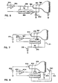
- Figure 6 a system similar to that shown in Figure 1 is shown except that the pixel input and fixed bias to the first grid and cathode, respectively, are reversed.
- the first grid 350 is connected to a source of fixed bias 352 and the variable pixel signal to produce the image to be copied is presented to an input 354 connected to pixel amplifier 356 whose output is connected through sensing resistor 358 to the cathode 360. Otherwise the compensation remains the same by controlling the bias to the second grid 362 from controller 364 which may be like that described in connection with Figure 3.
- FIG 7 a system similar to Figure 1 is shown except that the current indicative of brightness is produced across a sensing resistor 370 attached between the anode 371 of the CRT and the anode bias source 372.
- the cathode 373 is again connected to a source of fixed potential at 374, the pixel input 376 is again connected to the first grid 378 through the pixel amplifier 380 like in Figure 1 but these two connections could be reversed as in Figure 6.
- the compensation is again provided by controlling the bias to the second grid 382 with a controller which may be like that described in connection with Figure 3.
- FIG 8 a system similar to Figure 1 is shown but now the brightness is sensed by a photo sensor 390 set to view the output from the face of the CRT.
- the brightness controls the input to the controller 392, in a manner similar to the input from the sensing resistor R S in Figure 1, via leads 394 and 396 and again the bias to the second grid 398 is controlled to assure consistent brightness.
- the pixel input 400 is again connected to the first grid 402 through pixel amplifier 404 and the cathode 406 is again connected to a source of fixed potential 408 as these elements were connected in Figure 7, but again they could be reversed.
Landscapes
- Engineering & Computer Science (AREA)
- Multimedia (AREA)
- Signal Processing (AREA)
- Television Receiver Circuits (AREA)
- Testing, Inspecting, Measuring Of Stereoscopic Televisions And Televisions (AREA)
Claims (17)
- Dispositif de compensation de dérive pour la commande de la luminosité d'une image produite par un CRT (tube à rayons cathodiques) (70) pourvu d'une anode, d'une cathode (72), d'une première grille (74) et d'une seconde grille (76), la cathode (72) étant reliée à une source d'un premier potentiel et la première grille (74) étant reliée à un deuxième potentiel et étant disposée entre ladite cathode et ladite seconde grille, caractérisé par
un moyen de détection (88) destiné à délivrer ledit deuxième potentiel et, en outre, pour délivrer une tension de sortie qui est représentative de la luminosité de l'image, ladite tension de sortie étant seulement appliquée à la seconde grille (76) dans le but de compenser la dérive, dans lequel des variations de luminosité dues à la dérive sont détectées par ledit moyen de détection (88) afin de produire des variations de ladite tension de sortie, alors que ledit deuxième potentiel reste inchangé, de façon à faire varier la luminosité afin de compenser la dérive. - Dispositif selon la revendication 1, dans lequel ledit moyen de détection (88) détecte le courant circulant dans la cathode (72).
- Dispositif selon la revendication 1, dans lequel ledit moyen de détection détecte le courant circulant dans l'anode (figure 7).
- Dispositif selon la revendication 1, dans lequel ledit moyen de détection (390) est sensible au rayonnement (390) de l'image (figure 8).
- dispositif selon la revendication 2, dans lequel ledit moyen de détection de courant comprend une impédance (86) reliée dans le cheminement du courant de la cathode (72), et dans lequel la tension à travers ladite impédance est détectée.
- dispositif selon la revendication 3, dans lequel l'anode est reliée en série avec une impédance (370) et une source d'un troisième potentiel (372), et dans lequel ladite tension à travers ladite impédance est détectée.
- Dispositif selon la revendication 5, dans lequel une sortie (118) correspondant à ladite tension à travers ladite impédance (86) est comparée à une référence, et le résultat de la comparaison (156) est utilisé pour régler la tension appliquée sur la seconde grille (76).
- Dispositif selon la revendication 2, comprenant, en outre, un moyen de modulation (128) destiné à moduler la tension appliquée sur l'une ou l'autre de la première grille (74) et de la cathode (72) de façon que le courant circulant dans lequel moyen de détection (88) présente une composante alternative.
- Dispositif selon la revendication 8, dans lequel ledit moyen de détection (88) comprend des moyens capacitifs (94, 96) destinés à ne laisser passer seulement que la composante alternative vers la sortie (78).
- Dispositif selon la revendication 9, comprenant, en outre, un moyen de détermination et de comparaison (124) pour déterminer la valeur crête à crête de la sortie alternative (118) et pour comparer la valeur crête à crête avec une valeur de référence.
- Dispositif selon la revendication 9 ou la revendication 10, comprenant, en outre, un moyen de numérisation (120) destiné à numériser la sortie (118) et à comparer la sortie numérisée à une valeur de référence numérisée afin de produire un signal numérique de différence, et comprenant un moyen de conversion D/A (numérique/analogique) (158) afin de convertir ledit signal numérique de différence en un signal analogique destiné à faire varier le potentiel appliqué sur la seconde grille (76).
- Dispositif selon la revendication 1, dans lequel le CRT (70) dispose de périodes produisant une image et ne produisant pas d'image et comprend un moyen de traitement (124) destiné à faire varier la tension appliquée sur la seconde grille (76) pendant la période ne produisant pas d'image jusqu'à ce qu'une valeur prédéterminée de la luminosité soit obtenue et ensuite à maintenir ladite tension sur la seconde grille (76) pendant la période produisant une image.
- Dispositif selon la revendication 2 ou la revendication 3 en combinaison avec la revendication 12, dans lequel ladite valeur prédéterminée de la luminosité est obtenue en détectant un courant prédéterminé correspondant.
- Dispositif selon la revendication 12 ou la revendication 13, dans lequel ladite valeur prédéterminée est une valeur légèrement au-dessus du courant de coupure (73).
- Dispositif selon la revendication 1, dans lequel, pendant une période produisant une image, l'un desdits premier et deuxième potentiels est égal à une valeur prédéterminée alors que l'autre est variable afin de produire l'image.
- Dispositif selon la revendication 12, dans lequel ledit moyen de traitement (124) comprend, en outre, un moyen de production de tension alternative pouvant être commandé pendant la période ne produisant pas d'image pour faire en sorte que le potentiel appliqué à l'une de la première grille et cathode oscille depuis une valeur inférieure à celle qui est nécessaire pour produire la coupure jusqu'à une valeur légèrement supérieure à celle qui est nécessaire pour produire la coupure.
- Dispositif selon la revendication 16, dans lequel ledit moyen de production de tension alternative provoque en premier l'abaissement de la tension appliquée à la seconde grille (76) à une valeur nécessaire pour assurer que la luminosité est située au-dessous de la coupure et ensuite l'augmentation de la tension appliquée sur la seconde grille (76) jusqu'à ce qu'une valeur prédéterminée de la luminosité soit détectée.
Applications Claiming Priority (2)
| Application Number | Priority Date | Filing Date | Title |
|---|---|---|---|
| US07/515,062 US5077502A (en) | 1990-04-26 | 1990-04-26 | Compensation for drift in a cathode ray tube |
| US515062 | 1990-04-26 |
Publications (3)
| Publication Number | Publication Date |
|---|---|
| EP0454086A2 EP0454086A2 (fr) | 1991-10-30 |
| EP0454086A3 EP0454086A3 (en) | 1992-04-22 |
| EP0454086B1 true EP0454086B1 (fr) | 1996-03-20 |
Family
ID=24049822
Family Applications (1)
| Application Number | Title | Priority Date | Filing Date |
|---|---|---|---|
| EP91106589A Expired - Lifetime EP0454086B1 (fr) | 1990-04-26 | 1991-04-24 | Compensation de dérive dans un tube cathodique |
Country Status (6)
| Country | Link |
|---|---|
| US (1) | US5077502A (fr) |
| EP (1) | EP0454086B1 (fr) |
| JP (1) | JPH06125511A (fr) |
| CA (1) | CA2041019A1 (fr) |
| DE (1) | DE69118010T2 (fr) |
| HK (1) | HK1006485A1 (fr) |
Families Citing this family (7)
| Publication number | Priority date | Publication date | Assignee | Title |
|---|---|---|---|---|
| FR2680932B1 (fr) * | 1991-08-30 | 1993-11-26 | Sextant Avionique | Dispositif d'asservissement de la tension de blocage d'un tube cathodique par double boucle. |
| DE4402865A1 (de) * | 1993-01-30 | 1994-08-04 | Samsung Electronics Co Ltd | Gittersperrschaltung |
| US5682087A (en) * | 1995-03-09 | 1997-10-28 | Hughes-Jvc Technology Corporation | Cathode current stabilization |
| KR100202317B1 (ko) * | 1996-10-09 | 1999-06-15 | 윤종용 | 화면 밝기 자동 보정 장치 및 방법 |
| DE10140038A1 (de) * | 2001-08-16 | 2003-02-27 | Siemens Ag | Verfahren sowie Schaltungsanordnung zum Betreiben einer monochromen Kathodenstrahlröhre bei einem vorbestimmten Kathoden-Arbeitspunkt |
| US6798155B2 (en) | 2002-05-15 | 2004-09-28 | Lg. Philips Display Co., Ltd. | Color image display device |
| US20120242412A1 (en) * | 2011-03-25 | 2012-09-27 | Peter Fletcher-Haynes | Auto Bias |
Family Cites Families (11)
| Publication number | Priority date | Publication date | Assignee | Title |
|---|---|---|---|---|
| US3441663A (en) * | 1965-05-04 | 1969-04-29 | Photo Electronics Corp | Non-linear amplifiers and systems |
| US4070691A (en) * | 1975-04-28 | 1978-01-24 | Thomson-Csf Laboratories, Inc. | Stabilizing system for cathode ray tube |
| US4075485A (en) * | 1976-05-06 | 1978-02-21 | General Electric Company | Apparatus for controlling and displaying scintillation camera information |
| NL7709969A (nl) * | 1977-09-12 | 1979-03-14 | Philips Nv | Kleuren beeldweergeefinrichting met een schake- ling voor het opwekken van een schermroosterspan- ning. |
| US4300074A (en) * | 1979-04-13 | 1981-11-10 | Honeywell Inc. | Video coupling system |
| US4449501A (en) * | 1980-12-31 | 1984-05-22 | Lucas Industries Limited | Device for adjusting engine timing |
| US4442458A (en) * | 1982-03-29 | 1984-04-10 | Tektronix, Inc. | CRT Video drive circuit with beam current stabilization |
| US4461983A (en) * | 1982-10-15 | 1984-07-24 | Eastman Kodak Company | Stabilizing a transducer output |
| GB8414451D0 (en) * | 1984-06-06 | 1984-07-11 | Motorola Inc | Crt control circuit |
| US4701679A (en) * | 1985-08-23 | 1987-10-20 | Hitachi, Ltd. | Method of and apparatus for controlling amount of electron beam in image pickup tube |
| US4742397A (en) * | 1986-01-16 | 1988-05-03 | Polaroid Corporation | System and method for adjusting image brightness in electronic printer |
-
1990
- 1990-04-26 US US07/515,062 patent/US5077502A/en not_active Expired - Lifetime
-
1991
- 1991-04-23 CA CA002041019A patent/CA2041019A1/fr not_active Abandoned
- 1991-04-24 EP EP91106589A patent/EP0454086B1/fr not_active Expired - Lifetime
- 1991-04-24 DE DE69118010T patent/DE69118010T2/de not_active Expired - Fee Related
- 1991-04-26 JP JP3123123A patent/JPH06125511A/ja active Pending
-
1998
- 1998-06-19 HK HK98105707A patent/HK1006485A1/en not_active IP Right Cessation
Also Published As
| Publication number | Publication date |
|---|---|
| DE69118010T2 (de) | 1996-11-07 |
| EP0454086A2 (fr) | 1991-10-30 |
| HK1006485A1 (en) | 1999-02-26 |
| DE69118010D1 (de) | 1996-04-25 |
| US5077502A (en) | 1991-12-31 |
| CA2041019A1 (fr) | 1991-10-27 |
| EP0454086A3 (en) | 1992-04-22 |
| JPH06125511A (ja) | 1994-05-06 |
Similar Documents
| Publication | Publication Date | Title |
|---|---|---|
| EP0083176B1 (fr) | Système et dispositif pour la conversion de signaux vidéo en images sur un support d'enregistrement sensible à la lumière | |
| US5216497A (en) | Digital convergence apparatus including an extrapolating circuit | |
| US4490653A (en) | Deflection systems and ramp generators therefor | |
| US4286868A (en) | Photographic printer with automatic sensor calibration | |
| US4158859A (en) | Automatic control of iris and clamping voltage in video signal generator | |
| EP0454086B1 (fr) | Compensation de dérive dans un tube cathodique | |
| US4217608A (en) | Radiation scanning system | |
| DE69722370T2 (de) | Kompensation mit geschlossener Schleife für Grautondruckvorrichtungen | |
| HK1006485B (en) | Compensation for drift in a cathode ray tube | |
| US4730214A (en) | Method and apparatus for correlating video and film images produced from electronic data | |
| US4172659A (en) | Photographic printer with automatic sensor calibration | |
| JP3331162B2 (ja) | ディスプレイ装置の駆動電流を測定するための回路装置および該ディスプレイ装置の駆動およびバイアス方法 | |
| EP0231950A2 (fr) | Méthode de conversion analogique-numérique non-linéaire | |
| GB2206469A (en) | Controlling crt display beam brightness in accordance with local faceplate thickness | |
| EP0210627A2 (fr) | Système d'écriture de film avec commande en boucle fermée pour des images électroniques | |
| US5550598A (en) | Convergence adjustment circuit and projection type display apparatus | |
| US4707739A (en) | Automatic calibration circuit for monitoring device | |
| US5321524A (en) | Gray level compensator for picture recorder | |
| KR100225040B1 (ko) | 프로젝션 티브이(Projection TV)의 주변부 밝기 보정장치 | |
| US4461983A (en) | Stabilizing a transducer output | |
| US5223768A (en) | Data display apparatus with function for correcting effect of external magnetic field | |
| GB1585063A (en) | Display systems | |
| JPH03504305A (ja) | テレビ映画装置におけるドリフト修正 | |
| US2915582A (en) | Dynamic control circuit for cathode ray tubes | |
| KR20010039714A (ko) | 컷오프조정장치 |
Legal Events
| Date | Code | Title | Description |
|---|---|---|---|
| PUAI | Public reference made under article 153(3) epc to a published international application that has entered the european phase |
Free format text: ORIGINAL CODE: 0009012 |
|
| AK | Designated contracting states |
Kind code of ref document: A2 Designated state(s): DE FR GB |
|
| PUAL | Search report despatched |
Free format text: ORIGINAL CODE: 0009013 |
|
| RAP1 | Party data changed (applicant data changed or rights of an application transferred) |
Owner name: ALLIANT TECHSYSTEMS INC. |
|
| AK | Designated contracting states |
Kind code of ref document: A3 Designated state(s): DE FR GB |
|
| 17P | Request for examination filed |
Effective date: 19920911 |
|
| 17Q | First examination report despatched |
Effective date: 19941031 |
|
| GRAH | Despatch of communication of intention to grant a patent |
Free format text: ORIGINAL CODE: EPIDOS IGRA |
|
| GRAA | (expected) grant |
Free format text: ORIGINAL CODE: 0009210 |
|
| AK | Designated contracting states |
Kind code of ref document: B1 Designated state(s): DE FR GB |
|
| REF | Corresponds to: |
Ref document number: 69118010 Country of ref document: DE Date of ref document: 19960425 |
|
| RAP2 | Party data changed (patent owner data changed or rights of a patent transferred) |
Owner name: SIENNA IMAGING, INC. |
|
| ET | Fr: translation filed | ||
| PLBE | No opposition filed within time limit |
Free format text: ORIGINAL CODE: 0009261 |
|
| STAA | Information on the status of an ep patent application or granted ep patent |
Free format text: STATUS: NO OPPOSITION FILED WITHIN TIME LIMIT |
|
| 26N | No opposition filed | ||
| REG | Reference to a national code |
Ref country code: GB Ref legal event code: IF02 |
|
| PGFP | Annual fee paid to national office [announced via postgrant information from national office to epo] |
Ref country code: FR Payment date: 20020417 Year of fee payment: 12 |
|
| PGFP | Annual fee paid to national office [announced via postgrant information from national office to epo] |
Ref country code: GB Payment date: 20020724 Year of fee payment: 12 |
|
| PGFP | Annual fee paid to national office [announced via postgrant information from national office to epo] |
Ref country code: DE Payment date: 20020731 Year of fee payment: 12 |
|
| PG25 | Lapsed in a contracting state [announced via postgrant information from national office to epo] |
Ref country code: GB Free format text: LAPSE BECAUSE OF NON-PAYMENT OF DUE FEES Effective date: 20030424 |
|
| PG25 | Lapsed in a contracting state [announced via postgrant information from national office to epo] |
Ref country code: DE Free format text: LAPSE BECAUSE OF NON-PAYMENT OF DUE FEES Effective date: 20031101 |
|
| GBPC | Gb: european patent ceased through non-payment of renewal fee | ||
| PG25 | Lapsed in a contracting state [announced via postgrant information from national office to epo] |
Ref country code: FR Free format text: LAPSE BECAUSE OF NON-PAYMENT OF DUE FEES Effective date: 20031231 |
|
| REG | Reference to a national code |
Ref country code: FR Ref legal event code: ST |