EP0454111A1 - Appareillage pour la production de monocristaux de silicium - Google Patents
Appareillage pour la production de monocristaux de silicium Download PDFInfo
- Publication number
- EP0454111A1 EP0454111A1 EP91106673A EP91106673A EP0454111A1 EP 0454111 A1 EP0454111 A1 EP 0454111A1 EP 91106673 A EP91106673 A EP 91106673A EP 91106673 A EP91106673 A EP 91106673A EP 0454111 A1 EP0454111 A1 EP 0454111A1
- Authority
- EP
- European Patent Office
- Prior art keywords
- partition member
- light transmittance
- silica glass
- quartz crucible
- silicon
- Prior art date
- Legal status (The legal status is an assumption and is not a legal conclusion. Google has not performed a legal analysis and makes no representation as to the accuracy of the status listed.)
- Withdrawn
Links
Images


Classifications
-
- C—CHEMISTRY; METALLURGY
- C30—CRYSTAL GROWTH
- C30B—SINGLE-CRYSTAL GROWTH; UNIDIRECTIONAL SOLIDIFICATION OF EUTECTIC MATERIAL OR UNIDIRECTIONAL DEMIXING OF EUTECTOID MATERIAL; REFINING BY ZONE-MELTING OF MATERIAL; PRODUCTION OF A HOMOGENEOUS POLYCRYSTALLINE MATERIAL WITH DEFINED STRUCTURE; SINGLE CRYSTALS OR HOMOGENEOUS POLYCRYSTALLINE MATERIAL WITH DEFINED STRUCTURE; AFTER-TREATMENT OF SINGLE CRYSTALS OR A HOMOGENEOUS POLYCRYSTALLINE MATERIAL WITH DEFINED STRUCTURE; APPARATUS THEREFOR
- C30B15/00—Single-crystal growth by pulling from a melt, e.g. Czochralski method
- C30B15/10—Crucibles or containers for supporting the melt
- C30B15/12—Double crucible methods
-
- C—CHEMISTRY; METALLURGY
- C30—CRYSTAL GROWTH
- C30B—SINGLE-CRYSTAL GROWTH; UNIDIRECTIONAL SOLIDIFICATION OF EUTECTIC MATERIAL OR UNIDIRECTIONAL DEMIXING OF EUTECTOID MATERIAL; REFINING BY ZONE-MELTING OF MATERIAL; PRODUCTION OF A HOMOGENEOUS POLYCRYSTALLINE MATERIAL WITH DEFINED STRUCTURE; SINGLE CRYSTALS OR HOMOGENEOUS POLYCRYSTALLINE MATERIAL WITH DEFINED STRUCTURE; AFTER-TREATMENT OF SINGLE CRYSTALS OR A HOMOGENEOUS POLYCRYSTALLINE MATERIAL WITH DEFINED STRUCTURE; APPARATUS THEREFOR
- C30B13/00—Single-crystal growth by zone-melting; Refining by zone-melting
- C30B13/16—Heating of the molten zone
- C30B13/22—Heating of the molten zone by irradiation or electric discharge
-
- C—CHEMISTRY; METALLURGY
- C30—CRYSTAL GROWTH
- C30B—SINGLE-CRYSTAL GROWTH; UNIDIRECTIONAL SOLIDIFICATION OF EUTECTIC MATERIAL OR UNIDIRECTIONAL DEMIXING OF EUTECTOID MATERIAL; REFINING BY ZONE-MELTING OF MATERIAL; PRODUCTION OF A HOMOGENEOUS POLYCRYSTALLINE MATERIAL WITH DEFINED STRUCTURE; SINGLE CRYSTALS OR HOMOGENEOUS POLYCRYSTALLINE MATERIAL WITH DEFINED STRUCTURE; AFTER-TREATMENT OF SINGLE CRYSTALS OR A HOMOGENEOUS POLYCRYSTALLINE MATERIAL WITH DEFINED STRUCTURE; APPARATUS THEREFOR
- C30B15/00—Single-crystal growth by pulling from a melt, e.g. Czochralski method
- C30B15/14—Heating of the melt or the crystallised materials
Definitions
- the present invention relates to an apparatus for manufacturing silicon single crystals by the Czochralski method.
- the prior art shows a method in which a silicon starting material is continuously fed into a crucible having a double structure, thereby maintaining the surface level of the molten material constant (Laid-Open Patent No. 40-10184).
- a silicon starting material is continuously fed into a crucible having a double structure, thereby maintaining the surface level of the molten material constant
- the manufacture of high quality granular polycrystal silicon has recently become possible and it has been considered relatively easy to feed this granular silicon to the molten material continuously at a constant feed rate, thus leading to the publication, of some inventions and a paper (inventions of Laid-Open Patent Nos. 58-130195 and 63-95195 and Laid-Open Utility Model No. 59-141578 and the paper Ann. Rev. Mater. Sci. 1987, Vol. 17, P273-278).
- the invention disclosed in Laid-Open Patent No. 61-36197 employs a crucible of the double structure as well as a heat insulating material arranged above the outer material melting section and a separate heater arranged at the bottom of the crucible so as to promote the melting of the starting material supplied.
- this invention also involves no means for preventing the dissipation of heat from the contacting portion between the inner surface of the inner crucible and the molten silicon surface so as to prevent the occurrence of solidification.
- the heating by the heater at the bottom of the crucible decreases the temperature of another heater arranged along the side of the crucible thus promoting the occurrence of solidification.
- the heat dissipation from inside the partition tends to decrease the temperature of the molten material inside the partition, particularly the molten material contacting with the partition.
- the material of the partition is transparent silica glass having an emissivity considerably greater than that of the molten silicon and a great amount of heat is dissipated from the partition to the water-cooled cover above the crucible.
- the crucible being of the double structure, the convention of the molten silicon is limited and the temperature inside the partition has a lesser tendency to rise.
- the method to use cellular silica glass for a partition of crucible disclosed in Japanese Patent Laid Open Publication No. 2-13389 is revealed. Occuring solidification around periphery of partition can be prevented using aforementioned method. Nevertheless as described later, when using cellular silica glass for a partition, vibration by fluctuation of surface tension on the molten liquid around the interior and exterior of partition occurs and oxidation induced stacking fault which is equivalent to crystal defect frequently affords troubles.
- the present invention has been made to overcome the foregoing deficiencies in the prior art, and it is an object of the present invention to provide an apparatus for manufacturing silicon single crystals, more particularly, large cylindrical silicon single crystals of 12 to 30cm in diameter, in which a starting material, in granular or lumpy form, is continuously fed into a crucible containing the molten material and which is capable of preventing the occurrence of solidification at the contacting portion between a partition immersed in the crucible and the surface of the molten material inside the partition and the occurrence of OSF.
- the present invention has been made to solve the problems and accomplish the above object and thus there is provided an improved silicon single crystal manufacturing apparatus in which a rotating crucible containing molten silicon material is divided by a partition member formed with at least one small hole therethrough in such a manner that the partition member surrounds a large cylindrical silicon single crystal of 12 to 30cm in diameter, which is pulled while being rotated, and the molten material is moved smoothly through the hole, and the silicon signal crystal is grown from inside the partition member while continuously feeding the silicon material to the outer side of the partition member.
- the apparatus has the following essential features:
- the partition member and crucible are made from cellular silica glass.
- the partition member is formed of cellular silica glass having a cell content (volume percentage) of not less than 0.01% and not greater than 15%, and the quartz crucible has a cell content over 1.3 times greater than the cell content of the partition member.
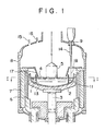
- Fig. 1 is a longitudinal sectional view showing schematically an embodiment of the present invention.
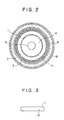
- Fig. 2 is a sectional view taken along the line I-I of Fig. 1.
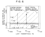
- Fig. 3 is a side view showing an embodiment of the partition member.
- Fig. 4a and 4b are diagrams for comparing the operations of the transparent silica glass and the cellular silica glass.
- Fig. 5 illustrates schematic diagrams for explaining the principle of the occurrence of ripples on the surface of molten silicon
- Fig. 6 is a graph showing schematically the relation between the degree of ripples and the light transmittance of silica glass with the temperature of the molten silicon near the silica glass as a parameter.
- Numeral 1 designates a crucible, 2 a graphite crucible, 3 a pedestal, 4 molten material, 5 a silicon single crystal, 6 a heater, 7 a heat insulating material, 8 a chamber, 11 a partition member, 12 cells, 13 a small hole, 14 a starting material feeder, 15 and 16 temperature detectors, 17 a heat insulating cover, 18 feed material, 22 starting material melting section, 23 crystal growing section.
- FIG. 5 there are illustrated schematic diagrams showing, respectively, the conditions in which transparent silica glass 21a and cellular silica glass 11a are immersed in molten material.
- the transparent silica glass 21a shown in Fig. 5a it will be seen that the contacting portion between the molten material 4 and the glass 21a is transparent and, therefore, the amount of heat dissipated from the molten material surface through the glass is increased.
- the heat dissipation of the transparent silica glass 21a is so large that the portion of the molten material 4 contacting with the glass 21a is decreased in temperature and the solidification tends to occur at this portion.
- the presence of cells 12 in the glass has the effect of scattering the dissipation of heat from the contacting portion between the molten material 4 and the cellular silica glass 11a and thus the heat dissipated from the molten material surface through the glass 11a is decreased as compared with the transparent silica glass 21a. Also, the cooling due to the heat transmission is reduced by the presence of the cells. As a result, in the portion of the molten material 4 contacting with the cellular silica glass 11a is not practically decreased in temperature and thus the molten material 4 prevented from solidifying. These effects are basically produced due to the reduced light transmittance.
- Fig. 1 is a sectional view showing schematically an embodiment of the present invention and Fig. 2 is a sectional view taken along the line I-I of Fig. 1.
- numeral 1 designates a silica crucible set in a graphite crucible 2, and the graphite crucible 2 is vertically movably and rotatably supported on a pedestal 3.
- Numeral 4 designates molten silicon materials contained in the crucible 1, and a silicon single crystal 5 grown into a large cylindrical form of 12 to 30cm in diameter is pulled from the molten silicon material 4.
- Numeral 6 designates a heater surrounding the graphite crucible 2, and 7 a hot-zone heat insulating material surrounding the heater 6.
- Number 11 designates a partition member made from a cellular high-purity silica glass and arranged concentrically with the crucible 1, and at least one small hole 13 is formed through its region below substantially the central portion in the height direction as shown by way of example in Fig. 3.
- the partition member 11 is set, along with the starting material, in the crucible 1 so that after the starting material has been melted, the partition member is immersed in the molten material 4 so as to surround the signal crystal 5 and its upper portion is exposed from the molten material surface. Also, its lower edge portion is practically fused to the crucible 1 and therefore it is prevented from floating. As a result, the molten material 4 outside the partition member 11 is moved to the inner side thereof only through the small hole 13. It is to be noted that the partition member 11 may be preliminarily fused to the crucible 1.
- Numeral 9 designates an opening formed in a chamber 8 in correspondence to the molten material surface outside the partition member 11, and fixedly inserted into the opening 9 is a feeder 14 for feeding a starting material in granular or lumpy form.
- the forward end of the feeder 14 is in opposition to the molten material surface outside the partition member 11.
- the feeder 14 is connected to a starting material feed chamber (not shown) arranged outside the chamber 8 thereby continuously feeding the granular or lumpy starting material.
- Numerals 15 and 16 designate temperature detectors such as radiation thermometers arranged in the upper part of the chamber 8 so that the temperature detector 15 measures the temperature of the molten material surface outside the partition member 11 and the other temperature detector 16 measures the temperature of the molten material inside thereof.
- Numeral 17 designates a heat insulating cover which in this embodiment is provided to enhance further the heat insulating effect on the partition member 11 although the cellular silica glass partition member 11 itself has a function of preventing the occurrence of solidification.
- the partition member 11 is made from cellular silica glass
- the heat dissipation from the contacting portion between the inner surface of the partition member 11 and the molten silicon material 4 is decreased to prevent solidification of the molten material at the partition member 11.
- This solidification preventing effect on the molten material 4 by the cellular silica glass is caused usually with a cell content (volume percentage) of 0.01% or over.
- the solidification preventing effect on molten material can be similarly obtained if new cells are formed by the heat for melting the silicon material or if the cell content (volume percentage) is increased to greater than 0.01%, due to the expansion of the already existing cells.
- the growing of a silicon single crystal is effected using cellular silica glass having a cell content (volume percentage of preferably between 0.01 and 15%.)
- a silicon single crystal manufacturing apparatus of the present invention in which a rotating crucible containing molten silicon material is divided by a partition member formed with at least one small hole therethrough in such a manner that the partition member surrounds a large cylindrical silicon crystal of 12 to 30cm in diameter which is pulled while being rotated and the molten silicon material is movable smoothly and the silicon single crystal is grown inside the partition member while feeding starting silicon material continuously to the outer side of the partition member, the whole or part of the partition member is made from cellular silica glass so that the dissipation of heat from the molten material near the partition member is reduced and the molten material is prevented from being solidified from its portion contacting with the partition member, thereby pulling the sound silicon single crystal.
- the working of the present invention has great effects that the yield is improved due to the uniform quality in the pulling direction of a silicon single crystal, that the improved productivity is attained.
- the use of the cellular silica glass reduces the temperature variation and wettability variation of the meniscus portion where the molten silicon and the partition member make contact with each other.
- the occurrence of ripples on the molten silicon surface is reduced by a mechanism which will be described later.
- This smoothening of the molten silicon surface has a very great effect on improving the quality of the crystal (the reduction of OSF (oxidation induced staking fault).
- OSF oxidation induced staking fault
- the reason is that the crystal growth is considerably stabilized. That which has a direct effect on the OSF is the occurrence of ripples on the surface of the molten silicon in the single crystal growing section.
- the occurrence of large ripples in the starting material melting section is not desirable since these ripples are propagated to the single crystal growing section through the communication hole formed through the partition member.
- the foregoing improvement of the crystal quality constitutes a second feature of the present invention.
- the cell content of the partition member is selected to be from 0.01% to 15% and 1/1.3 or less of the cell content of the quartz crucible whereby the light transmittance of the partition member is in a range from 5/1000 to 40/100 times the light transmittance of non-cellular silica glass and it is also over 2 times the light transmittance of the quartz crucible. If the previously mentioned temperature variation and wettability variation of the meniscus portion exists, ripples are caused on the molten silicon surface by the following mechanism.
- the molten silicon is a liquid having a relatively large surface tension. It is known that generally the surface tension is a function of temperature and the surface tension is decreased with an increase in the temperature.
- Fig. 5a illustrates a schematic diagram of the contacting portion between the molten silicon and the silica glass partition member 11.
- the molten silicon in a starting material melting section 22 is high in temperature and it serves the role of supplying heat to the molten silicon in a single crystal growing section 23.
- a careful consideration is to be made about the temperature of the molten silicon at around the meniscus portion where the molten silicon in the single crystal growing section 23 and the partition member 11 contact with each other.
- the light transmittance is the ratio of transmitted light intensity to incident light intensity when the light transmission rate of non-cellular silica glass is taken as 1.
- the lower limit is 5/1000. If the light transmittance is less than 5/1000, the surface irregularities and the internal cells are increased excessively and the danger of the broken pieces of silica entering the molten silicon becomes extremely great.
- the light transmittance is decreased with an increase in the content of the cells in the silica glass. This is due to the scattering of light by the cells. If the cell content (volume percentage) is selected 0.01 or over, the light transmittance is reduced to 40/100 or less.
- the upper limit of the cell content is 15%. The reason is that if the cell content exceeds 15%, the pieces of the broken glass come off and thus the probability of the silicon single crystal being polycrystallized becomes extremely high.
- the surface of the silica glass may be formed with irregularities.
- the light transmittance is decreased with increase in the peak density of the irregularities.
- the light transmittance can also be varied by varying the degree of the surface roughness. In other words, the transmittance can be adjusted by adjusting the peak density and the roughness.
- the practical peak line density ppi peak/inch is in a range between 10 and 25000 and range of roughness is from 1 ⁇ m to 2000 ⁇ m in terms of r.m.s.
- first and second methods may be combined for the purpose of decreasing the light transmittance.
- the second problem is the ripples on the molten silicon surface in the starting material melting section.
- the cause is the same as in the case of the partition member. Since the ripples are caused in the contacting portion between the quartz crucible and the molten silicon, the source of input heat to the molten silicon is the graphite crucible of a higher temperature.
- the second problem differs in this respect from the case of the partition.
- the molten silicon temperature of the starting material melting section is apparently higher than the molten silicon temperature in the single crystal growing section and the occurrence of larger ripples than in the case of the partition member is observed.
- the countermeasure is also to decrease the light transmittance of the silica glass forming the crucible.
- Fig. 6 shows schematically the relation between the degree of ripples and the light transmittance of the silica glass.
- the temperature of the molten silicon near the silica glass is used as a parameter.
- the broken lines represent the isotherms. Where the molten silicon temperature is constant, the ripples become smaller with decrease in the light transmittance. Also, where the light transmittances are the same, it is indicated that the ripples are larger when the molten silicon temperature is higher.
- the molten silicon temperature near the partition on the single crystal growing section side is T + 10°C.
- the light transmittance in order to reduce the ripples on the molten silicon surface, the light transmittance must be 20/100 or less. Since the reduced transmittance means the rough surface or the increased cells, there is the greater danger of the broken silica pieces entering the molten silicon.
- the upper limit of the tolerance limit should preferably be selected for the light transmittance. Namely, the light transmittance of 20/100 is the best in this case.
- the molten silicon temperature of the starting material melting section is higher than the molten silicon temperature of the single crystal growing section as mentioned previously, it is assumed that the molten silicon temperature of the starting material melting section is higher than that of the single crystal growing section by 20°C.
- the light transmittance of the quartz crystal is 20/100 which is the same with that of the partition member, larger ripples are caused near the quartz crucible in the starting material melting section.
- the light transmittance of the quartz crucible must be lower than the light transmittance of the partition member.
- the reduced ripple condition can also be produced in the starting material melting section if the light transmittance of the quartz crucible is less than 1/2 of that of the partition member or less than 10/100 in this case.
- the same methods as used for reducing the light transmittance of the partition member can be used as the methods for reducing the light transmittance of the quartz crucible.
- the cell content of the quartz crucible can be increased to over 1.3 times the cell content (volume percentage) of the partition member so as to reduce the light transmittance of the quartz crucible to 1/2 or less of that of the partition member.
- the peak density of the irregularities can be increased as compared with that of the partition member, thereby reducing the light transmittance of the quartz crucible to 1/2 or less of that of the partition member.
- the range of practical peak line densities ppi peak/inch is from 10 to 25000 as in the case of the partition member and the range of degrees of roughness is from 1 ⁇ m to 2000 ⁇ m in terms of r.m.s.
- Crystals were grown by the apparatus of Fig. 1 and the relation between the materials of the partition member and the crucible and the OSF density was examined.
- the principal growing conditions other than the materials of the partition member and the crucible were as follows: Crystal diameter, 6 inches; crucible diameter, 20 inches, crucible revolutions, 10 r.p.m.; crystal revolutions, 20 r.p.m.; heat keeping cover thickness, tantalum sheet of 0.2mm.
- the rate of light transmittance of the non-cellular glass was used the value of 80/100 on the supposition that the value in vacuum was 1.
Landscapes
- Chemical & Material Sciences (AREA)
- Engineering & Computer Science (AREA)
- Crystallography & Structural Chemistry (AREA)
- Materials Engineering (AREA)
- Metallurgy (AREA)
- Organic Chemistry (AREA)
- Crystals, And After-Treatments Of Crystals (AREA)
- Liquid Deposition Of Substances Of Which Semiconductor Devices Are Composed (AREA)
Applications Claiming Priority (2)
| Application Number | Priority Date | Filing Date | Title |
|---|---|---|---|
| JP2114523A JPH0825833B2 (ja) | 1990-04-27 | 1990-04-27 | シリコン単結晶の製造方法 |
| JP114523/90 | 1990-04-27 |
Publications (1)
| Publication Number | Publication Date |
|---|---|
| EP0454111A1 true EP0454111A1 (fr) | 1991-10-30 |
Family
ID=14639887
Family Applications (1)
| Application Number | Title | Priority Date | Filing Date |
|---|---|---|---|
| EP91106673A Withdrawn EP0454111A1 (fr) | 1990-04-27 | 1991-04-25 | Appareillage pour la production de monocristaux de silicium |
Country Status (6)
| Country | Link |
|---|---|
| EP (1) | EP0454111A1 (fr) |
| JP (1) | JPH0825833B2 (fr) |
| KR (1) | KR940004639B1 (fr) |
| CN (1) | CN1055964A (fr) |
| FI (1) | FI911127A7 (fr) |
| MY (1) | MY104640A (fr) |
Families Citing this family (14)
| Publication number | Priority date | Publication date | Assignee | Title |
|---|---|---|---|---|
| JPH0612477U (ja) * | 1992-07-24 | 1994-02-18 | 三菱マテリアル株式会社 | 引上装置 |
| JP3533416B2 (ja) * | 1996-02-06 | 2004-05-31 | 三菱住友シリコン株式会社 | 単結晶引上装置 |
| DE19917288C2 (de) * | 1999-04-16 | 2001-06-28 | Heraeus Quarzglas | Quarzglas-Tiegel |
| US7141768B2 (en) | 2000-04-28 | 2006-11-28 | Nexicor, Llc | Fastening device |
| DE10102126A1 (de) * | 2001-01-18 | 2002-08-22 | Wacker Siltronic Halbleitermat | Verfahren und Vorrichtung zum Herstellen eines Einkristalls aus Silicium |
| JP4651119B2 (ja) * | 2007-02-22 | 2011-03-16 | 信越石英株式会社 | シリコン単結晶引き上げ用大口径石英ガラスるつぼ |
| JP5008695B2 (ja) * | 2008-06-30 | 2012-08-22 | ジャパンスーパークォーツ株式会社 | 石英ガラスルツボおよび石英ガラスルツボを用いたシリコン単結晶の引き上げ方法 |
| JP5226754B2 (ja) * | 2010-10-08 | 2013-07-03 | 信越石英株式会社 | シリコン単結晶引き上げ用大口径石英ガラスるつぼの製造方法 |
| CN103739567B (zh) * | 2014-02-08 | 2016-09-21 | 山东省农药科学研究院 | 一种2-氯-5-氯甲基噻唑晶型及制备方法 |
| US10060046B2 (en) * | 2014-09-19 | 2018-08-28 | Corner Star Limited | Crystal puller for inhibiting melt contamination |
| CN112243493B (zh) * | 2018-05-17 | 2024-08-27 | 胜高股份有限公司 | 石英坩埚的透过率测定方法及装置 |
| JP7006636B2 (ja) * | 2019-03-01 | 2022-01-24 | 株式会社Sumco | シリコン単結晶製造装置 |
| US12146236B2 (en) * | 2021-06-07 | 2024-11-19 | Globalwafers Co., Ltd | Use of quartz plates during growth of single crystal silicon ingots |
| CN116536761A (zh) * | 2023-05-31 | 2023-08-04 | 西安奕斯伟材料科技股份有限公司 | 母合金的制作方法、坩埚组件和单晶炉 |
Citations (2)
| Publication number | Priority date | Publication date | Assignee | Title |
|---|---|---|---|---|
| EP0283903A2 (fr) * | 1987-03-20 | 1988-09-28 | Mitsubishi Materials Corporation | Procédé pour la fabrication d'un double creuset en quartz et procédé pour la fabrication d'une barre en silicium monocristallin |
| FR2625513A1 (fr) * | 1987-12-31 | 1989-07-07 | Westinghouse Electric Corp | Creusets perfectionnes pour le tirage d'une bande dendritique de silicium |
-
1990
- 1990-04-27 JP JP2114523A patent/JPH0825833B2/ja not_active Expired - Fee Related
-
1991
- 1991-03-06 FI FI911127A patent/FI911127A7/fi not_active Application Discontinuation
- 1991-03-22 MY MYPI91000482A patent/MY104640A/en unknown
- 1991-04-02 CN CN91102023A patent/CN1055964A/zh active Pending
- 1991-04-04 KR KR1019910005434A patent/KR940004639B1/ko not_active Expired - Lifetime
- 1991-04-25 EP EP91106673A patent/EP0454111A1/fr not_active Withdrawn
Patent Citations (2)
| Publication number | Priority date | Publication date | Assignee | Title |
|---|---|---|---|---|
| EP0283903A2 (fr) * | 1987-03-20 | 1988-09-28 | Mitsubishi Materials Corporation | Procédé pour la fabrication d'un double creuset en quartz et procédé pour la fabrication d'une barre en silicium monocristallin |
| FR2625513A1 (fr) * | 1987-12-31 | 1989-07-07 | Westinghouse Electric Corp | Creusets perfectionnes pour le tirage d'une bande dendritique de silicium |
Also Published As
| Publication number | Publication date |
|---|---|
| FI911127L (fi) | 1991-10-28 |
| CN1055964A (zh) | 1991-11-06 |
| KR910018582A (ko) | 1991-11-30 |
| KR940004639B1 (ko) | 1994-05-27 |
| FI911127A7 (fi) | 1991-10-28 |
| JPH0412088A (ja) | 1992-01-16 |
| FI911127A0 (fi) | 1991-03-06 |
| MY104640A (en) | 1994-04-30 |
| JPH0825833B2 (ja) | 1996-03-13 |
Similar Documents
| Publication | Publication Date | Title |
|---|---|---|
| US5009863A (en) | Apparatus for manufacturing silicon single crystals | |
| US5139750A (en) | Silicon single crystal manufacturing apparatus | |
| KR930003044B1 (ko) | 실리콘 단결정의 제조방법 및 장치 | |
| KR20060009304A (ko) | 인화인듐 기판 및 인화인듐 단결정과 그 제조 방법 | |
| KR940004639B1 (ko) | 실리콘 단결정 제조장치 | |
| US5370078A (en) | Method and apparatus for crystal growth with shape and segregation control | |
| US5143704A (en) | Apparatus for manufacturing silicon single crystals | |
| US5114528A (en) | Edge-defined contact heater apparatus and method for floating zone crystal growth | |
| US4944925A (en) | Apparatus for producing single crystals | |
| US4957712A (en) | Apparatus for manufacturing single silicon crystal | |
| EP0516014B1 (fr) | Monocristaux de rutile et leur procédés de croissance | |
| JPH06227891A (ja) | シリコン単結晶引上げ用ルツボ | |
| US5667585A (en) | Method for the preparation of wire-formed silicon crystal | |
| US5089082A (en) | Process and apparatus for producing silicon ingots having high oxygen content by crucible-free zone pulling, silicon ingots obtainable thereby and silicon wafers produced therefrom | |
| JPH04154687A (ja) | 半導体単結晶製造装置 | |
| EP0355833B1 (fr) | Méthode de production d'un monocristal de composé semi-conducteur | |
| US3567397A (en) | Apparatus for obtaining a dross-free crystalline growth melt | |
| JP2883910B2 (ja) | 単結晶シリコンの製造方法 | |
| JP2755452B2 (ja) | シリコン単結晶の引上げ装置 | |
| JP2734820B2 (ja) | 化合物半導体単結晶の製造方法 | |
| JP3079991B2 (ja) | 単結晶の製造装置および製造方法 | |
| JPH0316989A (ja) | シリコン単結晶の製造装置 | |
| JPH0259494A (ja) | シリコン単結晶の製造方法及び装置 | |
| JPH01286994A (ja) | シリコン単結晶の製造方法及び装置 | |
| JPH05124887A (ja) | 単結晶の製造方法及びその装置 |
Legal Events
| Date | Code | Title | Description |
|---|---|---|---|
| PUAI | Public reference made under article 153(3) epc to a published international application that has entered the european phase |
Free format text: ORIGINAL CODE: 0009012 |
|
| AK | Designated contracting states |
Kind code of ref document: A1 Designated state(s): DE FR GB IT NL |
|
| 17P | Request for examination filed |
Effective date: 19920207 |
|
| 17Q | First examination report despatched |
Effective date: 19940110 |
|
| STAA | Information on the status of an ep patent application or granted ep patent |
Free format text: STATUS: THE APPLICATION IS DEEMED TO BE WITHDRAWN |
|
| 18D | Application deemed to be withdrawn |
Effective date: 19940521 |