EP0454134A2 - Halbleiteranordnung - Google Patents
Halbleiteranordnung Download PDFInfo
- Publication number
- EP0454134A2 EP0454134A2 EP91106723A EP91106723A EP0454134A2 EP 0454134 A2 EP0454134 A2 EP 0454134A2 EP 91106723 A EP91106723 A EP 91106723A EP 91106723 A EP91106723 A EP 91106723A EP 0454134 A2 EP0454134 A2 EP 0454134A2
- Authority
- EP
- European Patent Office
- Prior art keywords
- semiconductor device
- input buffer
- bonding pads
- pads
- assembly
- Prior art date
- Legal status (The legal status is an assumption and is not a legal conclusion. Google has not performed a legal analysis and makes no representation as to the accuracy of the status listed.)
- Ceased
Links
Images



Classifications
-
- G—PHYSICS
- G11—INFORMATION STORAGE
- G11C—STATIC STORES
- G11C5/00—Details of stores covered by group G11C11/00
- G11C5/06—Arrangements for interconnecting storage elements electrically, e.g. by wiring
-
- G—PHYSICS
- G11—INFORMATION STORAGE
- G11B—INFORMATION STORAGE BASED ON RELATIVE MOVEMENT BETWEEN RECORD CARRIER AND TRANSDUCER
- G11B19/00—Driving, starting, stopping record carriers not specifically of filamentary or web form, or of supports therefor; Control thereof; Control of operating function ; Driving both disc and head
- G11B19/02—Control of operating function, e.g. switching from recording to reproducing
- G11B19/04—Arrangements for preventing, inhibiting, or warning against double recording on the same blank or against other recording or reproducing malfunctions
-
- G—PHYSICS
- G11—INFORMATION STORAGE
- G11B—INFORMATION STORAGE BASED ON RELATIVE MOVEMENT BETWEEN RECORD CARRIER AND TRANSDUCER
- G11B19/00—Driving, starting, stopping record carriers not specifically of filamentary or web form, or of supports therefor; Control thereof; Control of operating function ; Driving both disc and head
- G11B19/20—Driving; Starting; Stopping; Control thereof
-
- G—PHYSICS
- G11—INFORMATION STORAGE
- G11B—INFORMATION STORAGE BASED ON RELATIVE MOVEMENT BETWEEN RECORD CARRIER AND TRANSDUCER
- G11B27/00—Editing; Indexing; Addressing; Timing or synchronising; Monitoring; Measuring tape travel
- G11B27/10—Indexing; Addressing; Timing or synchronising; Measuring tape travel
- G11B27/19—Indexing; Addressing; Timing or synchronising; Measuring tape travel by using information detectable on the record carrier
- G11B27/28—Indexing; Addressing; Timing or synchronising; Measuring tape travel by using information detectable on the record carrier by using information signals recorded by the same method as the main recording
- G11B27/30—Indexing; Addressing; Timing or synchronising; Measuring tape travel by using information detectable on the record carrier by using information signals recorded by the same method as the main recording on the same track as the main recording
- G11B27/3027—Indexing; Addressing; Timing or synchronising; Measuring tape travel by using information detectable on the record carrier by using information signals recorded by the same method as the main recording on the same track as the main recording used signal is digitally coded
-
- G—PHYSICS
- G11—INFORMATION STORAGE
- G11B—INFORMATION STORAGE BASED ON RELATIVE MOVEMENT BETWEEN RECORD CARRIER AND TRANSDUCER
- G11B7/00—Recording or reproducing by optical means, e.g. recording using a thermal beam of optical radiation by modifying optical properties or the physical structure, reproducing using an optical beam at lower power by sensing optical properties; Record carriers therefor
- G11B7/007—Arrangement of the information on the record carrier, e.g. form of tracks, actual track shape, e.g. wobbled, or cross-section, e.g. v-shaped; Sequential information structures, e.g. sectoring or header formats within a track
- G11B7/00745—Sectoring or header formats within a track
-
- G—PHYSICS
- G11—INFORMATION STORAGE
- G11B—INFORMATION STORAGE BASED ON RELATIVE MOVEMENT BETWEEN RECORD CARRIER AND TRANSDUCER
- G11B7/00—Recording or reproducing by optical means, e.g. recording using a thermal beam of optical radiation by modifying optical properties or the physical structure, reproducing using an optical beam at lower power by sensing optical properties; Record carriers therefor
- G11B7/08—Disposition or mounting of heads or light sources relatively to record carriers
- G11B7/085—Disposition or mounting of heads or light sources relatively to record carriers with provision for moving the light beam into, or out of, its operative position or across tracks, otherwise than during the transducing operation, e.g. for adjustment or preliminary positioning or track change or selection
- G11B7/08505—Methods for track change, selection or preliminary positioning by moving the head
- G11B7/08529—Methods and circuits to control the velocity of the head as it traverses the tracks
-
- G—PHYSICS
- G11—INFORMATION STORAGE
- G11B—INFORMATION STORAGE BASED ON RELATIVE MOVEMENT BETWEEN RECORD CARRIER AND TRANSDUCER
- G11B7/00—Recording or reproducing by optical means, e.g. recording using a thermal beam of optical radiation by modifying optical properties or the physical structure, reproducing using an optical beam at lower power by sensing optical properties; Record carriers therefor
- G11B7/08—Disposition or mounting of heads or light sources relatively to record carriers
- G11B7/085—Disposition or mounting of heads or light sources relatively to record carriers with provision for moving the light beam into, or out of, its operative position or across tracks, otherwise than during the transducing operation, e.g. for adjustment or preliminary positioning or track change or selection
- G11B7/0857—Arrangements for mechanically moving the whole head
-
- G—PHYSICS
- G11—INFORMATION STORAGE
- G11B—INFORMATION STORAGE BASED ON RELATIVE MOVEMENT BETWEEN RECORD CARRIER AND TRANSDUCER
- G11B7/00—Recording or reproducing by optical means, e.g. recording using a thermal beam of optical radiation by modifying optical properties or the physical structure, reproducing using an optical beam at lower power by sensing optical properties; Record carriers therefor
- G11B7/24—Record carriers characterised by shape, structure or physical properties, or by the selection of the material
- G11B7/2407—Tracks or pits; Shape, structure or physical properties thereof
- G11B7/24085—Pits
-
- G—PHYSICS
- G11—INFORMATION STORAGE
- G11C—STATIC STORES
- G11C29/00—Checking stores for correct operation ; Subsequent repair; Testing stores during standby or offline operation
- G11C29/006—Checking stores for correct operation ; Subsequent repair; Testing stores during standby or offline operation at wafer scale level, i.e. wafer scale integration [WSI]
-
- G—PHYSICS
- G11—INFORMATION STORAGE
- G11C—STATIC STORES
- G11C29/00—Checking stores for correct operation ; Subsequent repair; Testing stores during standby or offline operation
- G11C29/04—Detection or location of defective memory elements, e.g. cell constructio details, timing of test signals
- G11C29/08—Functional testing, e.g. testing during refresh, power-on self testing [POST] or distributed testing
- G11C29/12—Built-in arrangements for testing, e.g. built-in self testing [BIST] or interconnection details
- G11C29/1201—Built-in arrangements for testing, e.g. built-in self testing [BIST] or interconnection details comprising I/O circuitry
-
- G—PHYSICS
- G11—INFORMATION STORAGE
- G11C—STATIC STORES
- G11C29/00—Checking stores for correct operation ; Subsequent repair; Testing stores during standby or offline operation
- G11C29/04—Detection or location of defective memory elements, e.g. cell constructio details, timing of test signals
- G11C29/08—Functional testing, e.g. testing during refresh, power-on self testing [POST] or distributed testing
- G11C29/48—Arrangements in static stores specially adapted for testing by means external to the store, e.g. using direct memory access [DMA] or using auxiliary access paths
-
- G—PHYSICS
- G11—INFORMATION STORAGE
- G11C—STATIC STORES
- G11C5/00—Details of stores covered by group G11C11/00
-
- G—PHYSICS
- G11—INFORMATION STORAGE
- G11C—STATIC STORES
- G11C5/00—Details of stores covered by group G11C11/00
- G11C5/06—Arrangements for interconnecting storage elements electrically, e.g. by wiring
- G11C5/066—Means for reducing external access-lines for a semiconductor memory clip, e.g. by multiplexing at least address and data signals
-
- G—PHYSICS
- G11—INFORMATION STORAGE
- G11C—STATIC STORES
- G11C7/00—Arrangements for writing information into, or reading information out from, a digital store
- G11C7/10—Input/output [I/O] data interface arrangements, e.g. I/O data control circuits, I/O data buffers
- G11C7/1078—Data input circuits, e.g. write amplifiers, data input buffers, data input registers, data input level conversion circuits
-
- G—PHYSICS
- G11—INFORMATION STORAGE
- G11C—STATIC STORES
- G11C7/00—Arrangements for writing information into, or reading information out from, a digital store
- G11C7/10—Input/output [I/O] data interface arrangements, e.g. I/O data control circuits, I/O data buffers
- G11C7/1078—Data input circuits, e.g. write amplifiers, data input buffers, data input registers, data input level conversion circuits
- G11C7/1084—Data input buffers, e.g. comprising level conversion circuits, circuits for adapting load
-
- G—PHYSICS
- G11—INFORMATION STORAGE
- G11C—STATIC STORES
- G11C7/00—Arrangements for writing information into, or reading information out from, a digital store
- G11C7/10—Input/output [I/O] data interface arrangements, e.g. I/O data control circuits, I/O data buffers
- G11C7/1078—Data input circuits, e.g. write amplifiers, data input buffers, data input registers, data input level conversion circuits
- G11C7/109—Control signal input circuits
Definitions
- the present invention relates to a semiconductor device and, more particularly, to a bonding pad.
- non-defective chips are selected and defective chips are marked by a die sort test after manufacture process of a wafer, and then the non-defective chips are packaged into a finished product.
- the needle of a probe card of a prober may be brought into contact with a bonding pad on an integrated circuit chip region of the wafer except when the die sort test is carried out.
- a bonding pad which is connected to word lines of a memory integrated circuit through switching elements, is formed and, before the die sort test is performed, a voltage is applied to the bonding pad by bringing the needle of the probe card into contact with the bonding pad and a voltage stress is applied to the word lines through the switching elements, thereby screening defective memory cells.
- An object of the present invention is to provide a semiconductor device capable of resolving the abovedescribed problem in which the yield of assembly deteriorates as the contact of the needle of a probe card with a bonding pad increases in number.
- a semiconductor device comprising a plurality of bonding pads having the same function and serving as one of grouped terminals other than a power supply terminal.
- the bonding pads are selectively used from the end of the manufacture process of wafers to the assembly process, and the number of times of contact of the needle of the probe card with the bonding pads, which are used (to which wires are bonded) in the assembly process, is less than that in the conventional semiconductor device. The yield of assembly is thus improved.
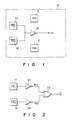
- Fig. 1 is a circuit diagram partially showing a dynamic random access memory (DRAM) according to the first embodiment of the present invention.
- DRAM dynamic random access memory
- Bonding pads 2 serving as power supply terminals for receiving power supply potential V CC and ground potential V SS , grouped terminals other than the power supply terminals, and various types of circuits are formed on a chip 1a of the DRAM.
- a plurality of bonding pads (first pad 11 and second pad 12) is formed to function as one of the grouped terminals.
- the pads 11 and 12 are connected in common to an input terminal of an input buffer circuit (e.g., inverter circuit).
- the probe card is put into contact with the second pad 12 to apply a signal or a voltage thereto and, in this case, the first pad 11 is not used.
- wires are bonded to the first pad 11 and, in this case, the second pad 12 is not used.
- a row address strobe (RAS) terminal receiving a RAS signal is used as one of the foregoing pads for use in the screening of defective cells on the wafer.
- RAS row address strobe
- a bit line precharge signal generator circuit is activated to generate a bit line precharge signal.
- the bit line precharge signal generator circuit is thus turned on, and all bit lines of a memory cell array are precharged with a predetermined bit line potential. If the RAS signal is activated, a word line is selected in response to an address signal. It is therefore necessary to inactivate the RAS signal input to the RAS terminal when an operating power supply voltage is applied to the DRAM chip regions on the wafer and the screening test for defective memory cells is carried out in a conductive state of the bit line precharge signal generator circuit.
- all word lines of the memory cell array are automatically and sequentially selected by designating a column address strobe (CAS) before RAS refresh mode. If an operating power supply voltage is applied to the DRAM chip regions on the wafer to activate a CAS signal and a RAS signal in sequence and thus the CAS before RAS refresh mode is designated, a voltage stress can be sequentially applied to all word lines in the DRAM chip regions and the screening test for defective memory cells on the wafer can be carried out.
- CAS column address strobe
- the needle of the probe card is simply and reliably brought into contact with the second pad 12, which is not used for assembly, even in a chip which is out of view of a microscope.
- the second pad 12 has only to be formed larger than the first pad 11 which is used for assembly.
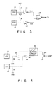
- Fig. 2 is a circuit diagram partially showing a DRAM according to the second embodiment of the present invention.
- the first and second pads 11 and 12 are connected to their corresponding first and second input buffer circuits (e.g., inverter circuits) 21 and 22 to receive input signals IN1 and IN2 , respectively.
- Output signals in1 and in2 of the first and second input buffer circuits 21 and 22 are supplied to a logic circuit (e.g., NOR gate circuit) 23.
- An output signal of the logic circuit 23 is then supplied to the internal circuit of the DRAM as an input signal.
- the DRAM having the circuit shown in Fig. 2 has the same advantage as that of the DRAM shown in Fig. 1. Further, since the two pads 11 and 12 are not connected to their common input buffer circuit but to different input buffer circuits 21 and 22, the capacitance of the pads 11 and 12 is separated and therefore these pads are not affected by each other.
- Fig. 3 is a circuit diagram partially showing a DRAM according to the third embodiment of the present invention.
- a resistor R having high resistance is connected between a high potential node (e.g., power supply potential V CC ) and each of the pads 11 and 12 receiving a control signal ( RAS ), the high level “H” of which represents a standby state and the low level “L” of which represents an active state. It is thus possible to prevent one of the pads having the same function, which is used, from adversely influencing the other pad.
- a high potential node e.g., power supply potential V CC
- RAS control signal
- the resistor R can be connected between a low potential node (e.g., ground potential V SS ) and each of the pads 11 and 12.
- V SS ground potential
- Signal terminals receiving a signal whose high and low levels “H” and “L” correspond to “1” and “0” respectively, can be used in a circuit as shown in Fig. 4.
- Fig. 4 is a circuit diagram partially showing a DRAM according to the fourth embodiment of the present invention.
- the pads 11 and 12 having the same function as that of one address terminal are each connected to the ground potential V SS through the resistor R, and an address signal Ain input to the pad 11 or 12 is received by the gate of n-channel enhancement type MOS transistor 51 or 52 and then supplied to an input buffer circuit 53.
- the sources of the MOS transistors 51 and 52 are connected to the ground potential V SS , and the drains thereof are connected in common to an input terminal of the input buffer circuit 53.
- the drains of the transistors 51 and 52 are connected together to one of input terminals of the differential amplifier circuit.
- the drain of another n-channel enhancement type MOS transistor 54 is connected to the other input terminal of the differential amplifier circuit, and a reference potential Vref, which is set between the high and low levels "H” and “L”, is connected to the gate of the MOS transistor 54.
- the pads 11 and 12 have only to be connected to the power supply potential V CC through the resistor R in order to receive the address signal Ain by the gate of a p-channel enhancement type MOS transistor and then supply it to the input buffer circuit.
- Fig. 5 is a circuit diagram partially showing a DRAM according to the fifth embodiment of the present invention.
- the pads 11 and 12 having the same function as that of one of address terminals are connected together to an input terminal of an input buffer circuit 63 through switching elements such as transfer gates 61 and 62, corresponding to the pads, respectively, and output signals ain and ain , which are complementary to each other, are input to the internal circuit of the DRAM, such as an address decoder.
- the transfer gates 61 and 62 are selectively turned on. To control these transfer gates, signals input to the pads (not shown) having the same function as that of a signal terminal (not shown) other than the address terminal corresponding to the pads 11 and 12, can be used before the signals are combined together. More specifically, the control signals in1 and in2 shown in Figs. 2 and 3 or another signal produced from these control signals can be used.
- Fig. 6 is a circuit diagram partially showing a DRAM according to the sixth embodiment of the present invention.
- the pads 11 and 12 having the same function as that of one of address terminals are connected to their corresponding input buffer circuits 71 and 72, and output signals of the input buffer circuits, which are complementary to each other, are supplied through switching elements such as transfer gates 73 and 74 and combined together.
- the combined signals ain and ain are input to the internal circuit of the DRAM.
- the transfer gates 61, 62, 73 and 74 can be replaced with the other switching elements such as CMOS clocked inverter circuits.
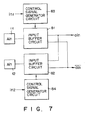
- Fig. 7 is a circuit diagram partially showing a DRAM according to the seventh embodiment of the present invention.
- reference numerals 81 and 82 denote input buffer circuits which are provided so as to correspond to the pads 11 and 12 having the same function as that of one of address terminals, and numerals 83 and 84 indicate control signal generator circuits for generating a control signal for separately controlling the active/inactive states of the input buffer circuits 81 and 82.
- Fig. 8 is a circuit diagram specifically showing the input buffer circuit 81 shown in Fig. 7.
- reference numerals P1 to P8 indicate P-channel MOS transistors; N1 to N16, N-channel MOS transistors; C1 to C4, MOS capacitors each having V SS potential to which the drain and source of each N-channel MOS transistor are connected in common; SA, a differential CMOS sense amplifier; Ain, an input signal; Vref, reference potential; in1 , in1', and HLD , gate control signals; LTC, a sense amplifier activation (latch) control signal; and ain and ain , output signals which are complementary to each other.
- Fig. 9 is a circuit diagram showing the control signal generator circuit 83 shown in Fig. 7.
- the control signal generator circuit generates the control signals in1 and in1'.
- reference numerals 91 and 92 denote CMOS inverter circuits, and in1 indicates the control signals as shown in, for example, Figs. 2 and 3.
- Fig. 10 is a view showing the arrangement of bonding pads on a chip of a DRAM according to an eighth embodiment of the present invention.
- reference numeral 100 indicates a wafer and numeral 1b denotes DRAM chip regions on the wafer.
- a plurality of pads having the same function is formed on each of the chip regions 1b so as to correspond to a plurality of terminals of a grouped terminals other than the power supply terminals, and a group of pads 12 of these pads, which are not used for assembly, are locally arranged on one side of the chip region 1b.
- the arrangement of the group of pads 12 not used for assembly is favorable for the screening test for defective memory cells on the wafer using a probe card, or the arrangement makes it easy to fabricate the probe card used for the screening test and to obtain a number of chip regions when the screening test for defective memory cells on the wafer is carried out.
- Fig. 11 is a view showing the arrangement of bonding pads on a chip region of the wafer of a DRAM according to a ninth embodiment of the present invention.
- a plurality of pairs of pads (11a, 12a), (11b, 12b), (11c, 12c), ..., (11x, 12x), (11y, 12y), and (11z, 12z) is formed on a chip 1c of the DRAM so as to correspond to a plurality of terminals of a grouped terminals other than the power supply terminal.
- One group of pads 11a, 11b, 11c, ..., 11x, 11y, and 11z are arranged on opposing sides of the chip, and the other group of pads 12a, 12b, 12c, ..., 12x, 12y, and 12z are arranged on another side of the chip.
- the pads 11a, 11b, 11c, ..., 11x, 11y, and 11z are used in a test or an operation other than the die sort test performed from the end of the wafer manufacture process to the assembly, and the pads 12a, 12b, 12c, ..., 12x, 12y, and 12z are used for the assembly.
- the pads 12a, 12b, 12c, ..., 12x, 12y, and 12z are used in the test or operation other than the die sort test performed from the end of the wafer manufacture process to the assembly, and the pads 11a, 11b, 11c, ..., 11x, 11y, and 11z are used for the assembly.
- the shape of the package meets the standards for the arrangement of external terminals in the SOJ or ZIP.
- three pads having the same function have only to be provided in accordance with the arrangement of the bonding pads shown in Fig. 11.
- One of the three pads is used in the test or operation other than the die sort test performed from the end of the wafer manufacture process to the assembly, and one of the other two pads is used for the assembly.
- the chip can thus be housed in the SOJ or ZIP.
- the semiconductor device according to the present invention is provided with a plurality of pads having the same function. Therefore, at least one of the pads can be used in the test or operation other than the die sort test performed from the end of the wafer manufacture process to the assembly and cannot be used for the assembly.
- the number of times of contact of the needle of a probe card with the pads used for assembly is less than that in the conventional semiconductor device.
- the yield of the assembly can thus be improved.
- a plurality of pads having the same function can be arranged so as to facilitate the arrangement of terminals of each package, so that the layout of leads of the package need not be unnecessarily contrived and, in this respect, the yield of assembly can be improved.
- the pads, which are not used for assembly, can be arranged in each of the chip regions. If the chip regions have the pads in common, a number of chip regions can be more easily obtained when the screening test for defective memory cells on the wafer is carried out. It is usual in this case that plural chip regions, which are exposed together by a wafer pattern exposure device such as a stepper, have in common pads not used for assembly. However, all the chip regions on the wafer have in common the pads not used for the assembly.
Landscapes
- Semiconductor Integrated Circuits (AREA)
- Dram (AREA)
- Testing Or Measuring Of Semiconductors Or The Like (AREA)
- For Increasing The Reliability Of Semiconductor Memories (AREA)
- Design And Manufacture Of Integrated Circuits (AREA)
- Semiconductor Memories (AREA)
Applications Claiming Priority (2)
| Application Number | Priority Date | Filing Date | Title |
|---|---|---|---|
| JP2107542A JP2531827B2 (ja) | 1990-04-25 | 1990-04-25 | 半導体装置及びその製造方法 |
| JP107542/90 | 1990-04-25 |
Publications (2)
| Publication Number | Publication Date |
|---|---|
| EP0454134A2 true EP0454134A2 (de) | 1991-10-30 |
| EP0454134A3 EP0454134A3 (en) | 1993-05-19 |
Family
ID=14461831
Family Applications (1)
| Application Number | Title | Priority Date | Filing Date |
|---|---|---|---|
| EP19910106723 Ceased EP0454134A3 (en) | 1990-04-25 | 1991-04-25 | Semiconductor device |
Country Status (4)
| Country | Link |
|---|---|
| US (1) | US5386127A (de) |
| EP (1) | EP0454134A3 (de) |
| JP (1) | JP2531827B2 (de) |
| KR (1) | KR960004460B1 (de) |
Families Citing this family (13)
| Publication number | Priority date | Publication date | Assignee | Title |
|---|---|---|---|---|
| KR100200916B1 (ko) * | 1995-11-16 | 1999-06-15 | 윤종용 | 웨이퍼 테스트 신호 발생기를 가지는 반도체 메모리 장치 |
| JP3019918B2 (ja) * | 1996-08-12 | 2000-03-15 | 日本電気株式会社 | 半導体集積回路及びその電源供給回路 |
| US6356958B1 (en) | 1999-02-08 | 2002-03-12 | Mou-Shiung Lin | Integrated circuit module has common function known good integrated circuit die with multiple selectable functions |
| US6180426B1 (en) | 1999-03-01 | 2001-01-30 | Mou-Shiung Lin | High performance sub-system design and assembly |
| JP2001358293A (ja) * | 2000-06-12 | 2001-12-26 | Toshiba Corp | 半導体装置 |
| JP5085829B2 (ja) * | 2002-05-07 | 2012-11-28 | メギカ・コーポレイション | 集積回路チップ構造 |
| JP2006324359A (ja) * | 2005-05-17 | 2006-11-30 | Elpida Memory Inc | 半導体チップ及び半導体装置 |
| KR100734290B1 (ko) | 2005-11-28 | 2007-07-02 | 삼성전자주식회사 | 출력 채널이 공유되는 테스트 패드를 구비하는 필름형반도체 패키지 및 필름형 반도체 패키지의 테스트 방법,테스트 채널이 공유되는 패턴을 구비하는 테스트 장치 및반도체 장치 그리고 반도체 장치에서의 테스트 방법 |
| KR101791829B1 (ko) | 2010-01-20 | 2017-10-31 | 가부시키가이샤 한도오따이 에네루기 켄큐쇼 | 휴대 전자 기기 |
| JP2012114241A (ja) * | 2010-11-25 | 2012-06-14 | Renesas Electronics Corp | 半導体チップおよび半導体装置 |
| KR101571985B1 (ko) * | 2011-07-05 | 2015-11-25 | 인텔 코포레이션 | 자체-불능 칩 이네이블 입력 |
| CN104113355B (zh) | 2013-04-19 | 2017-01-11 | 联发科技(新加坡)私人有限公司 | 一种电子装置 |
| JP7426702B2 (ja) * | 2020-02-13 | 2024-02-02 | ザインエレクトロニクス株式会社 | 半導体装置 |
Family Cites Families (15)
| Publication number | Priority date | Publication date | Assignee | Title |
|---|---|---|---|---|
| US4413271A (en) * | 1981-03-30 | 1983-11-01 | Sprague Electric Company | Integrated circuit including test portion and method for making |
| JPS59188956A (ja) * | 1983-04-11 | 1984-10-26 | Nec Corp | 半導体装置 |
| JPH0714002B2 (ja) * | 1984-05-15 | 1995-02-15 | セイコーエプソン株式会社 | チップへの信号供給方法 |
| JPS61222148A (ja) * | 1985-03-08 | 1986-10-02 | Fujitsu Ltd | 1チツプマイクロコンピユ−タの製造方法 |
| JPS61253847A (ja) * | 1985-05-02 | 1986-11-11 | Nec Corp | 高信頼度を有する半導体装置 |
| JP2605687B2 (ja) * | 1986-04-17 | 1997-04-30 | 三菱電機株式会社 | 半導体装置 |
| JPS62271443A (ja) * | 1986-05-20 | 1987-11-25 | Toshiba Corp | 半導体装置 |
| US4884122A (en) * | 1988-08-05 | 1989-11-28 | General Electric Company | Method and configuration for testing electronic circuits and integrated circuit chips using a removable overlay layer |
| JPS63128729A (ja) * | 1986-11-19 | 1988-06-01 | Nec Corp | 半導体ウエハ−プロ−バ−用ステ−ジ |
| JPS63128729U (de) * | 1987-02-14 | 1988-08-23 | ||
| JP2795846B2 (ja) * | 1987-11-25 | 1998-09-10 | 株式会社東芝 | 半導体装置 |
| JP2594988B2 (ja) * | 1987-11-27 | 1997-03-26 | 株式会社日立製作所 | 半導体集積回路装置の動作電位供給配線の配線設計方法 |
| US5008727A (en) * | 1988-01-22 | 1991-04-16 | Matsushita Electric Industrial Co., Ltd. | Standard cell having test pad for probing and semiconductor integrated circuit device containing the standard cells |
| JPH01278033A (ja) * | 1988-04-28 | 1989-11-08 | Nec Corp | 半導体集積回路のパッド配置構造 |
| JP2560805B2 (ja) * | 1988-10-06 | 1996-12-04 | 三菱電機株式会社 | 半導体装置 |
-
1990
- 1990-04-25 JP JP2107542A patent/JP2531827B2/ja not_active Expired - Fee Related
-
1991
- 1991-04-24 KR KR1019910006532A patent/KR960004460B1/ko not_active Expired - Fee Related
- 1991-04-25 EP EP19910106723 patent/EP0454134A3/en not_active Ceased
-
1994
- 1994-05-24 US US08/248,536 patent/US5386127A/en not_active Expired - Lifetime
Also Published As
| Publication number | Publication date |
|---|---|
| KR960004460B1 (ko) | 1996-04-06 |
| EP0454134A3 (en) | 1993-05-19 |
| JP2531827B2 (ja) | 1996-09-04 |
| KR910019236A (ko) | 1991-11-30 |
| JPH047853A (ja) | 1992-01-13 |
| US5386127A (en) | 1995-01-31 |
Similar Documents
| Publication | Publication Date | Title |
|---|---|---|
| US5212442A (en) | Forced substrate test mode for packaged integrated circuits | |
| KR950001133B1 (ko) | 스태틱형 반도체 기억장치 | |
| US4833650A (en) | Semiconductor memory device including programmable mode selection circuitry | |
| US6064557A (en) | Semiconductor device structured to be less susceptible to power supply noise | |
| US5386127A (en) | Semiconductor device having groups of pads which receive the same signal | |
| KR950001293B1 (ko) | 반도체 메모리칩의 병렬테스트 회로 | |
| KR100200916B1 (ko) | 웨이퍼 테스트 신호 발생기를 가지는 반도체 메모리 장치 | |
| JP3381929B2 (ja) | 半導体装置 | |
| US5282167A (en) | Dynamic random access memory | |
| US6496435B2 (en) | Sense amplifier control circuit of semiconductor memory device | |
| US6774655B2 (en) | Semiconductor device, method of testing the semiconductor device, and semiconductor integrated circuit | |
| US5255229A (en) | Dynamic random access memory including stress test circuitry | |
| KR19990029217A (ko) | 입력 신호의 오버슈트, 언더슈트를 피엔 접합을 이용한 회로에 의해 클램프하는 반도체 기억 장치 | |
| US6388926B1 (en) | Integrated circuit having forced substrate test mode with improved substrate isolation | |
| EP0488425A1 (de) | Halbleiter-Speichereinrichtung | |
| US5287012A (en) | Semiconductor integrated circuit equipped with diagnostic circuit for checking reference voltage signal supplied to internal step-down circuit | |
| US6021081A (en) | Semiconductor memory device having strobe buffer and output buffer | |
| US20030101374A1 (en) | Semiconductor device with reduced terminal input capacitance | |
| JP2003270302A (ja) | 半導体装置 | |
| JPH05274866A (ja) | 半導体装置 | |
| KR19980026104A (ko) | 전원 제어 회로 | |
| JPS5818711B2 (ja) | ハンドウタイキオクソウチノ デンアツセンスカイロ | |
| KR19980015271A (ko) | 반도체 메모리 장치의 번인(Burn-In) 스트레스 회로 및 그 방법 | |
| JPH02161691A (ja) | 半導体記憶装置 | |
| JPH04258880A (ja) | 半導体記憶装置 |
Legal Events
| Date | Code | Title | Description |
|---|---|---|---|
| PUAI | Public reference made under article 153(3) epc to a published international application that has entered the european phase |
Free format text: ORIGINAL CODE: 0009012 |
|
| 17P | Request for examination filed |
Effective date: 19910425 |
|
| AK | Designated contracting states |
Kind code of ref document: A2 Designated state(s): DE FR GB |
|
| PUAL | Search report despatched |
Free format text: ORIGINAL CODE: 0009013 |
|
| AK | Designated contracting states |
Kind code of ref document: A3 Designated state(s): DE FR GB |
|
| 17Q | First examination report despatched |
Effective date: 19941222 |
|
| STAA | Information on the status of an ep patent application or granted ep patent |
Free format text: STATUS: THE APPLICATION HAS BEEN REFUSED |
|
| 18R | Application refused |
Effective date: 19961226 |