EP0454246A1 - Phasenkorrekturschaltung für Signale in einem System mit doppelten digitalen Leitungen - Google Patents
Phasenkorrekturschaltung für Signale in einem System mit doppelten digitalen Leitungen Download PDFInfo
- Publication number
- EP0454246A1 EP0454246A1 EP91200949A EP91200949A EP0454246A1 EP 0454246 A1 EP0454246 A1 EP 0454246A1 EP 91200949 A EP91200949 A EP 91200949A EP 91200949 A EP91200949 A EP 91200949A EP 0454246 A1 EP0454246 A1 EP 0454246A1
- Authority
- EP
- European Patent Office
- Prior art keywords
- signal
- trb
- tra
- frame
- signals
- Prior art date
- Legal status (The legal status is an assumption and is not a legal conclusion. Google has not performed a legal analysis and makes no representation as to the accuracy of the status listed.)
- Granted
Links
- 230000005540 biological transmission Effects 0.000 claims abstract description 14
- 125000004122 cyclic group Chemical group 0.000 claims abstract description 6
- 230000000873 masking effect Effects 0.000 claims abstract description 5
- 230000001360 synchronised effect Effects 0.000 claims description 10
- 238000011144 upstream manufacturing Methods 0.000 claims description 5
- 230000001934 delay Effects 0.000 claims description 4
- 230000009977 dual effect Effects 0.000 claims description 4
- 238000001514 detection method Methods 0.000 claims description 3
- 230000003068 static effect Effects 0.000 claims description 3
- 210000000056 organ Anatomy 0.000 claims 1
- 230000003111 delayed effect Effects 0.000 abstract 1
- 238000010586 diagram Methods 0.000 description 9
- 230000010363 phase shift Effects 0.000 description 4
- 230000000694 effects Effects 0.000 description 3
- 230000006870 function Effects 0.000 description 3
- 230000001419 dependent effect Effects 0.000 description 2
- 230000009466 transformation Effects 0.000 description 2
- 230000015556 catabolic process Effects 0.000 description 1
- 238000004891 communication Methods 0.000 description 1
- 239000004020 conductor Substances 0.000 description 1
- 238000010276 construction Methods 0.000 description 1
- 230000000593 degrading effect Effects 0.000 description 1
- 238000005516 engineering process Methods 0.000 description 1
- 230000033764 rhythmic process Effects 0.000 description 1
- 230000000630 rising effect Effects 0.000 description 1
- 239000000126 substance Substances 0.000 description 1
Images


Classifications
-
- H—ELECTRICITY
- H04—ELECTRIC COMMUNICATION TECHNIQUE
- H04J—MULTIPLEX COMMUNICATION
- H04J3/00—Time-division multiplex systems
- H04J3/02—Details
- H04J3/06—Synchronising arrangements
- H04J3/062—Synchronisation of signals having the same nominal but fluctuating bit rates, e.g. using buffers
- H04J3/0626—Synchronisation of signals having the same nominal but fluctuating bit rates, e.g. using buffers plesiochronous multiplexing systems, e.g. plesiochronous digital hierarchy [PDH], jitter attenuators
- H04J3/0629—Synchronisation of signals having the same nominal but fluctuating bit rates, e.g. using buffers plesiochronous multiplexing systems, e.g. plesiochronous digital hierarchy [PDH], jitter attenuators in a network, e.g. in combination with switching or multiplexing, slip buffers
-
- H—ELECTRICITY
- H04—ELECTRIC COMMUNICATION TECHNIQUE
- H04L—TRANSMISSION OF DIGITAL INFORMATION, e.g. TELEGRAPHIC COMMUNICATION
- H04L1/00—Arrangements for detecting or preventing errors in the information received
- H04L1/02—Arrangements for detecting or preventing errors in the information received by diversity reception
Definitions
- the invention relates to a device for phasing signals on two digital channels each carrying a frame, respectively TRA and TRB, these frames conveying the same information but being affected by different delays, in a synchronous digital transmission system by information blocks, comprising, for each channel, a frame locking means which supplies a synchronization signal, from a low frequency superframe signal and a variable delay means controlled from said synchronization signal by a comparator of phase followed by a control unit.
- Any digital transmission system can be disturbed by a large number of causes, such as the imperfection of the transmission medium (radio beam for example), the presence of noise on the transmission channel, radio interference or breakdowns. These disturbances are reflected, from the point of view of the user, by an error rate on the digital bit rate used and by cut-off periods, which constitutes a general technical problem.
- a simple known solution to alleviate the general technical problem mentioned above consists in duplicating the signal to be transmitted, in transmitting it by two separate channels and in choose the better of the two signals on reception.
- the present invention is placed in this context of doubling of the digital path, a situation in which the particular problem of reshaping the two received signals can arise.
- This re-phasing allows, among other applications, switching from one signal to the other without causing clock loss errors of frame, and ... In these conditions, it becomes possible to pass from a frame signal TRA to a frame signal TRB as often as necessary, according to the respective errors in each frame, without risking degrading the transmission, and to exploit the maximum period of time, without error, of each digital path.
- the object of the invention is to effect a reshaping of signals from two precise digital frames simple and rapid by taking the synchronization signals from the frames upstream of the variable delay means.
- Another object of the invention is to effect a rephasing of two digital signals using variable delay means which also allow the simultaneous introduction of an additional fixed delay of predetermined value on the two signals.
- the signal phasing device defined in the preamble is remarkable in that said variable delay means are constituted by a common dual memory with cyclic addressing, each location contains a block of the TRA frame and a block of the TRB frame having the same rank in the frame, the addressing being carried out in writing by two separate write counters, each set on each synchronization signal and, in reading, from a read counter of each location that makes part of said control member, in that said frame locking means are connected to the input of the device, upstream of said double memory and in that said phase comparator is designed to select which of the two synchronization signals the most late and to transmit it to said controller, the information signals TRA ′ coming from the frame TRA and TRB ′ coming from the frame TRB at the output of said double memory being strictly synchronous.
- the device according to the invention is designed to operate in a synchronous environment where only the jitter problems of the clock signal occur which the invention takes into account. This makes it possible to get rid of a slaving mouth, complex and slow.
- the duration of the addressing cycle of the memory. double is equal to half a period of the super frame signal.
- the signal device is remarkable in that said control member which comprises said read counter further comprises a coincidence detector designed to compare a read synchronization signal which it receives from said read counter with said most late synchronization signal and to provide the read counter with a reload signal at a value shifted by a predetermined number M below the lower loading value of the two counter writing when the time offset between the two signals it receives exceeds a predetermined threshold proportional to the phase jitter, of the order of a few tens of bits.
- the memory is read with a fixed delay after the recording in memory of the latest signal.
- the device further comprises a switch which receives said synchronized information signals TRA 'and TRB', respectively from frames TRA and TRB, said switch being controlled from error detectors connected to the input of said phasing device, upstream from said double memory, and switching means which are designed to switch said switch on the input frame the least erroneous, and in that said predetermined number M implies in said double memory a fixed delay TF greater than the time necessary for the detection of errors in the frames TRA or TRB by said error detectors.
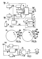
- Figure 1 is a block diagram of the signal phasing device according to the invention.
- FIGS. 2a and 2b are circular time diagrams illustrating the cyclic addressing of the double memory of FIG. 1.
- FIG. 3 represents in schematic form the phase comparator of FIG. 1.
- FIG. 4 represents the electronic diagram of an embodiment of the state machine of FIG. 3.
- FIGS. 5a and 5b which are time diagrams of the synchronization signals SYA and SYB and FIG. 5c which is a state diagram, make it possible to explain the operation of the state machine of FIG. 4.
- FIG. 6 is a time diagram illustrating the internal operation of the control member of FIG. 1.
- FIG. 7 is the block diagram of the phasing device according to the invention applied to the masking of transmission errors.
- FIG. 1 there are shown two digital channels (or paths) 1 and 2 which carry the frame signals TRA and TRB respectively carrying the same information but affected by different delays.
- This is for example, to fix the ideas of a time-division telephone transmission system at 2048 kbits / s, each frame comprising 32 telephone channels, at the rate of a sample coded on 8 bits for each channel, or frames of 256 bits.
- the maximum phase shift envisaged between the signals TRA and TRB is large and can reach several hundred frames. In the digital example envisaged, this maximum phase shift is for example equal to 256 frames, or 65,536 bits.
- the frame signal comprises, at regular time intervals, free bits which can be used in particular for recovering rhythms.
- the invention uses one of these bits to create a low-frequency superframe signal whose period T is at least equal to twice the maximum phase shift expressed in bit time (TBI).
- TTI bit time
- the frequency of the superframe signal is for example equal to 15 Hz.
- Each signal TRA, TRB is supplied on the one hand to a separate frame locking means 3, 4 and to common variable delay means 5 constituted by a double memory.
- the memory 5 is a circular memory of the static dual access RAM type.
- Each frame locking means 3, 4 of conventional design is designed to detect, in the frame signal, the pattern of the low-frequency superframe, to lock onto this pattern and provide a frame synchronization signal SYA, SYB under form of a square signal of period T.
- Each signal SYA, SYB is supplied to a counter 7, 8 and moreover, these two signals are also supplied to a phase comparator 9.
- the phase comparator 9 supplies a pulse signal SYC of period T to a control member 11 which is broken down into a read counter 12 and a coincidence detector 13, the latter receiving the signal SYC and a synchronization signal SYD of period T from the counter 12 and providing, in the event of phase coincidence of these two signals, a reloading signal SR, on a conductor 14, to the counter 12.
- the counters 7, 8, respectively 12, which are cyclic counters are used for the address writing age, respectively reading, of memory 5, by means of address buses 15, 16 for writing, and of a bus 17 for reading.
- a clock generator 18 supplies a clock signal H at the frequency of the data bits (of period TBI) to all the circuits of FIG.
- the clock signal H or, preferably, a derivative signal H 'at the frequency 1 / TBL of bytes or frames which represent data blocks is used for writing and reading the data blocks .
- Each write counter 7, 8 is calibrated on the synchronization signal SYA, SYB, its MSB (for example the weight 16) being activated at the frequency 1 / T and its LSB at the frequency of the data bits (signal H). It is possible, for the write and read addressing, to use all the significant bits of the counters as defined above, in which case the capacity of the memory 5 is equal to the number of data bits contained in a period T of the signal. superframe.
- the MSB is not used for addressing, which makes it possible to reduce the capacity of the memory 5 to half that indicated in the previous phase.
- Each location 19 of the memory is double and contains, just before being read, a block of TRA and a block of TRB, these two blocks having the same rank in the period defined by superframe signals which correspond in TRA and TRB , these two blocks therefore carrying the same information apart from transmission errors.
- the reading of each memory location provides, on two output terminals 23, 24, frame signals TRA ', TRB', strictly synchronous.
- the addressing of the memory 5 is shown in the form of a circle 26 on which, at a given instant t o controlled by the signal H ', the writing locations are pointed on the circle 26 by the arrows referenced WA, WB for the respective inscription of blocks different from the frames TRA and TRB, separated by a duration ⁇ t representative of the phase shift to be compensated.
- the reading is represented by the arrow R, offset with respect to the recording of the most late data signal by a predetermined number of blocks M x TBL (signal TRB in this case).
- the number M is chosen as low as possible when the application envisaged by the device does not provide for the introduction of a fixed delay through the memory 5.
- M is dependent on the mutual precision between the instants of writing and reading provided by the system, precision which is linked to phase jitter.
- FIG. 2b are represented time ranges of uncertainty ⁇ WA, ⁇ WB for writing and ⁇ R for reading. Under these conditions, the value of M must respect the following relation:
- FIG. 2a the following writing and reading cycle is represented by arrows in broken lines respectively close to arrows in solid line and counterparts of the latter.
- the remainder of the description essentially aims to describe how it is possible to achieve the delay M x TBL of the reading with respect to the writing of the most lagging signal among the data signals TRA and TRB.
- phase comparator 9 An embodiment of the phase comparator 9 is now described with reference to FIGS. 3, 4 and 5.
- the phase comparator represented in FIG. 3 comprises a state machine 28 which receives the synchronization signals SYA and SYB and supplies a logic signal SYR which carries the value "0" when SYB is behind delay on SYA (see FIG. 5a) and the value "1" otherwise (see Figure 5b).
- the SYR signal acts as a switch control signal. To this end, it is for example transmitted to an input of an AND logic gate circuit 29 which receives on a second input the signal SYA after transformation into impulse signal by circuit 30 and, by means of an inverter 31 to an input of an AND circuit 32 which also receives the signal SYB after transformation into impulse signal by circuit 34.
- the circuit 30, respectively 34 transforms the square signal SYA, respectively SYB into a pulse signal by monostable action on the rising edge or, preferably, on the falling edge of the square signal which it receives.
- the state machine 28 of FIG. 3 can be produced by means of the circuit of FIG. 4 which consists of five flip-flops D, 36 to 40, a NOR circuit (NOR) 42 and four NAND circuits (NAND) 44, 45, 46, 47. All the flip-flops receive the signal H on their clock input.
- the flip-flop 36 receives the signal SYA on its input D, its output Q is connected to the input D of the flip-flop 38 and to an input of the NAND 44, and its output Q is connected to an input of NAND 45.
- the flip-flop 37 receives the signal SYB on its input D, its output Q is connected to the input D of flip-flop 39 and to another input of NAND 45 and its output Q to another input of NAND 44.
- the output Q of flip-flops 38 and 39 is each connected to an input of NOR 42 whose output is connected to another input of NAND 44 and 45 respectively.
- the NANDs 46, 47 and the flip-flop 40 are linked in chain, in this order between the output of the NAND 44 and the output of the state machine carrying the signal SYR, and which identifies with the output Q of the flip-flop 40, this output being also looped back to another input of NAND 46 and the output of NAND 45 being connected to another input of NAND 47.
- FIG. 5c The circuit which has just been described produces the state diagram shown in FIG. 5c which can be read in conjunction with FIGS. 5a and 5b.
- the coincidence detector 13 receives the signal SYC, and the signal SYD from the read counter 12, signals which are represented in FIG. 6.
- the signal SYD which is synchronized with the counting cycle of the read counter with a predetermined delay close to the duration M x TBL (see FIG. 2a), has a low duty cycle, much less than 0 , 5 and is in the form of a pulse signal of the same period (T) as SYC but whose pulse duration is longer than that of SYC.
- the phasing device operates nominally as already described with reference to Figures 2a and 2b.
- the difference in pulse width is adjusted so as to be able to absorb the maximum jitter (of the order of a few tens of bits) which can occur between the clock signal H and the various signals present in the device, in particular between the SYC and SYD signals. If, on the other hand, the pulses of SYC and SYD do not coincide in time as is the case for example during power-up, a recharging signal SR in the form of a logic signal "1" or "O" is transmitted to the reset input (RESET) of counter 12, which has the effect of resetting the pulse of SYD to that of SYC and, simultaneously, restoring the counting of the reading addresses to their nominal value (FIG.
- REET reset input
- the counter is designed, by construction, to provide the optimal offset between read and write addresses when the signals SYC and SYD are, in substance, in phase.
- the design and arrangement of the circuits 12 and 13, and of the memory 5 for carrying out the simple functions described above are within the reach of those skilled in the art.
- the device of FIG. 1 is shown at 50, which receives on its two inputs the respective signals TRA and TRB and supplies the signals TRA 'and TRB' to the choice terminals of a switch 51 whose output is the seat of a signal S which is either the signal TRA '(as shown in the figure), or the signal TRB' depending on the position of the switch actuated by a signal SC on a control input.
- the device in FIG. 7 is intended for masking transmission errors.
- error detectors 53, 54 the inputs of which are connected respectively to the two inputs of the device 50 and which supply respective error signals to switching means 55.
- the switching means 55 are designed to compare the relative qualities of the frame signals TRA and TRB which it receives and, to transmit the control signal SC in the form of a logic signal 0 or 1 such that, at all times, the position of the switch 51 causes , at the output of the latter, the supply of the best among the two frame signals TRA 'or TRB'.
- the circuits 53, 54 and 55 are well known to those skilled in the art and do not require a detailed description.
- the number M is adjusted, at 50, so as to introduce a fixed delay TF greater than the time necessary for the detection of errors through the error detectors 53 and 54 increased by the time necessary by the comparison of errors in 55.
- memory 5 a static RAM memory of 256 kbits and integrate the other elements 3, 4, 7, 8, 9, 12, 13 and 18 in the form of a single integrated circuit.
Landscapes
- Engineering & Computer Science (AREA)
- Computer Networks & Wireless Communication (AREA)
- Signal Processing (AREA)
- Computer Hardware Design (AREA)
- Synchronisation In Digital Transmission Systems (AREA)
- Time-Division Multiplex Systems (AREA)
- Radio Transmission System (AREA)
- Detection And Prevention Of Errors In Transmission (AREA)
Applications Claiming Priority (2)
| Application Number | Priority Date | Filing Date | Title |
|---|---|---|---|
| FR9005411A FR2661579A1 (fr) | 1990-04-27 | 1990-04-27 | Dispositif de mise en phase de signaux dans un systeme a doublement du conduit numerique. |
| FR9005411 | 1990-04-27 |
Publications (2)
| Publication Number | Publication Date |
|---|---|
| EP0454246A1 true EP0454246A1 (de) | 1991-10-30 |
| EP0454246B1 EP0454246B1 (de) | 1995-08-02 |
Family
ID=9396179
Family Applications (1)
| Application Number | Title | Priority Date | Filing Date |
|---|---|---|---|
| EP91200949A Expired - Lifetime EP0454246B1 (de) | 1990-04-27 | 1991-04-22 | Phasenkorrekturschaltung für Signale in einem System mit doppelten digitalen Leitungen |
Country Status (5)
| Country | Link |
|---|---|
| US (1) | US5321727A (de) |
| EP (1) | EP0454246B1 (de) |
| JP (1) | JP3067832B2 (de) |
| DE (1) | DE69111669T2 (de) |
| FR (1) | FR2661579A1 (de) |
Cited By (4)
| Publication number | Priority date | Publication date | Assignee | Title |
|---|---|---|---|---|
| EP0744847A1 (de) * | 1995-05-23 | 1996-11-27 | Philips Communication D'entreprise | Redundantes Datenübertragungssystem mit mindestens zwei Kanälen |
| US6363055B1 (en) | 1997-05-06 | 2002-03-26 | D.S.P.C. Technologies Ltd. | Control channel determiner |
| US6847692B2 (en) | 2000-02-25 | 2005-01-25 | Fujitsu Limited | Data transmission system |
| RU2248672C2 (ru) * | 1999-02-24 | 2005-03-20 | Айбиквити Диджитал Корпорейшн | Способ смешивания звуковых сигналов, передатчик и приемник для цифрового звукового ам- и чм-вещания в полосе частот канала |
Families Citing this family (8)
| Publication number | Priority date | Publication date | Assignee | Title |
|---|---|---|---|---|
| US5633881A (en) * | 1993-02-22 | 1997-05-27 | Qualcomm Incorporated | Trellis encoder and decoder based upon punctured rate 1/2 convolutional codes |
| FR2715786A1 (fr) * | 1994-02-02 | 1995-08-04 | Trt Telecom Radio Electr | Système de transmission de données transmises par une liaison comprenant des équipements intermédiaires et équipement intermédiaire pour un tel système. |
| US5826014A (en) | 1996-02-06 | 1998-10-20 | Network Engineering Software | Firewall system for protecting network elements connected to a public network |
| US5898830A (en) * | 1996-10-17 | 1999-04-27 | Network Engineering Software | Firewall providing enhanced network security and user transparency |
| JP2000115263A (ja) * | 1998-09-30 | 2000-04-21 | Matsushita Electric Ind Co Ltd | ディジタル放送復調装置 |
| US8363744B2 (en) | 2001-06-10 | 2013-01-29 | Aloft Media, Llc | Method and system for robust, secure, and high-efficiency voice and packet transmission over ad-hoc, mesh, and MIMO communication networks |
| US7181538B2 (en) * | 2003-11-14 | 2007-02-20 | Sybase 365, Inc. | System and method for providing configurable, dynamic multimedia message service pre-transcoding |
| DE102017109192A1 (de) * | 2017-04-28 | 2018-10-31 | Technische Universität Darmstadt | Schaltungsanordnung und Verfahren zum Ermitteln eines Versatzes zwischen zwei Signalflanken |
Citations (2)
| Publication number | Priority date | Publication date | Assignee | Title |
|---|---|---|---|---|
| DE3107802A1 (de) * | 1981-02-28 | 1982-11-25 | Siemens AG, 1000 Berlin und 8000 München | "ausgleichersystem zum ausgleich von laufzeitschwankungen und festen rahmenverschiebungen" |
| EP0137563A2 (de) * | 1983-10-07 | 1985-04-17 | Telecommunications Radioelectriques Et Telephoniques T.R.T. | Umschaltungsverfahren mit automatischem Phasenausgleich der Daten über +/- 3,5 Bits und Vorrichtung zur Durchfürung des Verfahrens |
Family Cites Families (3)
| Publication number | Priority date | Publication date | Assignee | Title |
|---|---|---|---|---|
| US3628149A (en) * | 1968-12-19 | 1971-12-14 | Bell Telephone Labor Inc | Diversity switch for digital transmission |
| JPS5732535B2 (de) * | 1975-02-17 | 1982-07-12 | ||
| JPS54143009A (en) * | 1978-04-28 | 1979-11-07 | Kokusai Denshin Denwa Co Ltd | Space diversity system for tdma communication system |
-
1990
- 1990-04-27 FR FR9005411A patent/FR2661579A1/fr active Pending
-
1991
- 1991-04-22 DE DE69111669T patent/DE69111669T2/de not_active Expired - Fee Related
- 1991-04-22 EP EP91200949A patent/EP0454246B1/de not_active Expired - Lifetime
- 1991-04-24 JP JP3094192A patent/JP3067832B2/ja not_active Expired - Fee Related
- 1991-04-29 US US07/693,990 patent/US5321727A/en not_active Expired - Fee Related
Patent Citations (2)
| Publication number | Priority date | Publication date | Assignee | Title |
|---|---|---|---|---|
| DE3107802A1 (de) * | 1981-02-28 | 1982-11-25 | Siemens AG, 1000 Berlin und 8000 München | "ausgleichersystem zum ausgleich von laufzeitschwankungen und festen rahmenverschiebungen" |
| EP0137563A2 (de) * | 1983-10-07 | 1985-04-17 | Telecommunications Radioelectriques Et Telephoniques T.R.T. | Umschaltungsverfahren mit automatischem Phasenausgleich der Daten über +/- 3,5 Bits und Vorrichtung zur Durchfürung des Verfahrens |
Non-Patent Citations (1)
| Title |
|---|
| IBM TECHNICAL DISCLOSURE BULLETIN, vol. 17, no. 5, octobre 1964, page 371, New York, US; W.E. CONNORS: "Error controlled diversity combiner" * |
Cited By (5)
| Publication number | Priority date | Publication date | Assignee | Title |
|---|---|---|---|---|
| EP0744847A1 (de) * | 1995-05-23 | 1996-11-27 | Philips Communication D'entreprise | Redundantes Datenübertragungssystem mit mindestens zwei Kanälen |
| US5835483A (en) * | 1995-05-23 | 1998-11-10 | Bisson; Frederic | Information transmission system utilizing at least two channels in the redundancy mode |
| US6363055B1 (en) | 1997-05-06 | 2002-03-26 | D.S.P.C. Technologies Ltd. | Control channel determiner |
| RU2248672C2 (ru) * | 1999-02-24 | 2005-03-20 | Айбиквити Диджитал Корпорейшн | Способ смешивания звуковых сигналов, передатчик и приемник для цифрового звукового ам- и чм-вещания в полосе частот канала |
| US6847692B2 (en) | 2000-02-25 | 2005-01-25 | Fujitsu Limited | Data transmission system |
Also Published As
| Publication number | Publication date |
|---|---|
| JP3067832B2 (ja) | 2000-07-24 |
| JPH04229736A (ja) | 1992-08-19 |
| US5321727A (en) | 1994-06-14 |
| FR2661579A1 (fr) | 1991-10-31 |
| DE69111669D1 (de) | 1995-09-07 |
| EP0454246B1 (de) | 1995-08-02 |
| DE69111669T2 (de) | 1996-03-21 |
Similar Documents
| Publication | Publication Date | Title |
|---|---|---|
| EP0454246B1 (de) | Phasenkorrekturschaltung für Signale in einem System mit doppelten digitalen Leitungen | |
| EP0041429B1 (de) | Verfahren und Einrichtung zur Synchronisierung digitaler Signale | |
| EP0580234B1 (de) | Parallel-Seriell-Umsetzer | |
| EP0041001B1 (de) | Digitale Bit-für-Bit Zeitmultiplex-Fernmeldekoppelfelder | |
| EP2751637A1 (de) | Verfahren zur synchronisation eines serverclusters und dieses verfahren umsetzender servercluster | |
| CA1170772A (fr) | Procede et dispositif de codage de donnees binaires | |
| EP0454249B1 (de) | Dynamische Schaltungsanordnung zur Fehlermaskierung in einem System mit Verdoppelung des digitalen Kanals | |
| CA1269137A (fr) | Procede et dispositif de calage en phase de trains numeriques synchrones | |
| CA2046242C (fr) | Dispositif d'echantillonnage de donnees et systeme de transmission numerique de donnees en resultant | |
| EP0711049A1 (de) | Verfahren zur Referenzsymboldetektion in einem Emfängen für Digitaldaten | |
| EP0064923B1 (de) | System zur Phasensynchronisation digitaler Datenströme und seine Verwendung bei der Umschaltung der Datenströme | |
| EP0094040B1 (de) | System zur synchronen Datenübertragung mit Hilfe eines amplitudenmodulierten Trägers konstanter Hüllkurve | |
| EP0060751B1 (de) | Einrichtung zur Umschaltung von Datenübertragungsstrecken | |
| EP0056208A1 (de) | Verfahren und Einrichtung zur Synchronisation von Nachrichten | |
| FR2598869A1 (fr) | Detecteur de phase et de frequence, et son utilisation dans une boucle a verrouillage de phase | |
| CA2057942C (fr) | Systeme recepteur pour le traitement de signaux recus sur des voies de diversite | |
| FR2593008A1 (fr) | Procede et dispositif de regeneration de l'integrite du debit binaire dans un reseau plesiochrone | |
| EP0905946B1 (de) | Reglung der Abtastung von Biphasensignalen | |
| FR2721463A1 (fr) | Système de transmission comportant au moins deux liaisons pour relier un émetteur et un récepteur et récepteur convenant à un tel système. | |
| EP0643394B1 (de) | Schreib-/Lesetaktvergleichungsanordnung für einen Pufferspeicher | |
| EP0400734A1 (de) | Programmierbares Binärsignal-Verzögerungsverfahren und Anwendung auf ein Fehlerkorrigierkode-Verfahren | |
| FR2478912A1 (fr) | Memoire tampon, notamment pour un dispositif de contre-mesures electroniques | |
| EP0016678A1 (de) | Bittaktrückgewinnungs-Vorrichtung | |
| FR2564664A1 (fr) | Dispositif de recuperation d'un signal periodique | |
| EP4604444A1 (de) | Erzeugung eines taktsignals |
Legal Events
| Date | Code | Title | Description |
|---|---|---|---|
| PUAI | Public reference made under article 153(3) epc to a published international application that has entered the european phase |
Free format text: ORIGINAL CODE: 0009012 |
|
| AK | Designated contracting states |
Kind code of ref document: A1 Designated state(s): DE FR GB IT |
|
| RAP1 | Party data changed (applicant data changed or rights of an application transferred) |
Owner name: N.V. PHILIPS' GLOEILAMPENFABRIEKEN Owner name: TRT TELECOMMUNICATIONS RADIOELECTRIQUES ET TELEPHO |
|
| RAP1 | Party data changed (applicant data changed or rights of an application transferred) |
Owner name: N.V. PHILIPS' GLOEILAMPENFABRIEKEN Owner name: T.R.T. TELECOMMUNICATIONS RADIOELECTRIQUES ET TELE |
|
| K1C1 | Correction of patent application (title page) published |
Effective date: 19911030 |
|
| 17P | Request for examination filed |
Effective date: 19920429 |
|
| 17Q | First examination report despatched |
Effective date: 19940705 |
|
| GRAA | (expected) grant |
Free format text: ORIGINAL CODE: 0009210 |
|
| AK | Designated contracting states |
Kind code of ref document: B1 Designated state(s): DE FR GB IT |
|
| REF | Corresponds to: |
Ref document number: 69111669 Country of ref document: DE Date of ref document: 19950907 |
|
| ITF | It: translation for a ep patent filed | ||
| GBT | Gb: translation of ep patent filed (gb section 77(6)(a)/1977) |
Effective date: 19951102 |
|
| REG | Reference to a national code |
Ref country code: FR Ref legal event code: TP |
|
| PLBE | No opposition filed within time limit |
Free format text: ORIGINAL CODE: 0009261 |
|
| STAA | Information on the status of an ep patent application or granted ep patent |
Free format text: STATUS: NO OPPOSITION FILED WITHIN TIME LIMIT |
|
| 26N | No opposition filed | ||
| REG | Reference to a national code |
Ref country code: FR Ref legal event code: TP |
|
| REG | Reference to a national code |
Ref country code: FR Ref legal event code: CD |
|
| REG | Reference to a national code |
Ref country code: GB Ref legal event code: IF02 |
|
| PGFP | Annual fee paid to national office [announced via postgrant information from national office to epo] |
Ref country code: FR Payment date: 20030424 Year of fee payment: 13 |
|
| PGFP | Annual fee paid to national office [announced via postgrant information from national office to epo] |
Ref country code: GB Payment date: 20030430 Year of fee payment: 13 |
|
| PGFP | Annual fee paid to national office [announced via postgrant information from national office to epo] |
Ref country code: DE Payment date: 20030616 Year of fee payment: 13 |
|
| PG25 | Lapsed in a contracting state [announced via postgrant information from national office to epo] |
Ref country code: GB Free format text: LAPSE BECAUSE OF NON-PAYMENT OF DUE FEES Effective date: 20040422 |
|
| PG25 | Lapsed in a contracting state [announced via postgrant information from national office to epo] |
Ref country code: DE Free format text: LAPSE BECAUSE OF NON-PAYMENT OF DUE FEES Effective date: 20041103 |
|
| GBPC | Gb: european patent ceased through non-payment of renewal fee |
Effective date: 20040422 |
|
| PG25 | Lapsed in a contracting state [announced via postgrant information from national office to epo] |
Ref country code: FR Free format text: LAPSE BECAUSE OF NON-PAYMENT OF DUE FEES Effective date: 20041231 |
|
| REG | Reference to a national code |
Ref country code: FR Ref legal event code: ST |
|
| PG25 | Lapsed in a contracting state [announced via postgrant information from national office to epo] |
Ref country code: IT Free format text: LAPSE BECAUSE OF NON-PAYMENT OF DUE FEES;WARNING: LAPSES OF ITALIAN PATENTS WITH EFFECTIVE DATE BEFORE 2007 MAY HAVE OCCURRED AT ANY TIME BEFORE 2007. THE CORRECT EFFECTIVE DATE MAY BE DIFFERENT FROM THE ONE RECORDED. Effective date: 20050422 |