EP0454249A1 - Dynamische Schaltungsanordnung zur Fehlermaskierung in einem System mit Verdoppelung des digitalen Kanals - Google Patents
Dynamische Schaltungsanordnung zur Fehlermaskierung in einem System mit Verdoppelung des digitalen Kanals Download PDFInfo
- Publication number
- EP0454249A1 EP0454249A1 EP91200952A EP91200952A EP0454249A1 EP 0454249 A1 EP0454249 A1 EP 0454249A1 EP 91200952 A EP91200952 A EP 91200952A EP 91200952 A EP91200952 A EP 91200952A EP 0454249 A1 EP0454249 A1 EP 0454249A1
- Authority
- EP
- European Patent Office
- Prior art keywords
- fault
- memory
- signal
- signals
- switch
- Prior art date
- Legal status (The legal status is an assumption and is not a legal conclusion. Google has not performed a legal analysis and makes no representation as to the accuracy of the status listed.)
- Granted
Links
- 230000000873 masking effect Effects 0.000 title claims abstract description 12
- 230000015654 memory Effects 0.000 claims abstract description 64
- 230000005484 gravity Effects 0.000 claims abstract description 11
- 230000005540 biological transmission Effects 0.000 claims description 15
- 230000001934 delay Effects 0.000 claims description 3
- 230000006870 function Effects 0.000 description 7
- 238000010586 diagram Methods 0.000 description 6
- 238000001514 detection method Methods 0.000 description 5
- 230000010363 phase shift Effects 0.000 description 5
- 230000009471 action Effects 0.000 description 4
- 235000021183 entrée Nutrition 0.000 description 4
- 125000004122 cyclic group Chemical group 0.000 description 3
- 230000001360 synchronised effect Effects 0.000 description 3
- 239000004020 conductor Substances 0.000 description 2
- 238000010276 construction Methods 0.000 description 2
- 230000003111 delayed effect Effects 0.000 description 2
- 230000000694 effects Effects 0.000 description 2
- 210000000056 organ Anatomy 0.000 description 2
- 230000008901 benefit Effects 0.000 description 1
- 230000015556 catabolic process Effects 0.000 description 1
- 210000004027 cell Anatomy 0.000 description 1
- 238000004891 communication Methods 0.000 description 1
- 230000007547 defect Effects 0.000 description 1
- 230000000593 degrading effect Effects 0.000 description 1
- 230000009977 dual effect Effects 0.000 description 1
- 230000008030 elimination Effects 0.000 description 1
- 238000003379 elimination reaction Methods 0.000 description 1
- 230000006872 improvement Effects 0.000 description 1
- 238000012423 maintenance Methods 0.000 description 1
- 230000000630 rising effect Effects 0.000 description 1
- 230000003068 static effect Effects 0.000 description 1
- 239000000126 substance Substances 0.000 description 1
- 230000007704 transition Effects 0.000 description 1
Images


Classifications
-
- H—ELECTRICITY
- H04—ELECTRIC COMMUNICATION TECHNIQUE
- H04L—TRANSMISSION OF DIGITAL INFORMATION, e.g. TELEGRAPHIC COMMUNICATION
- H04L1/00—Arrangements for detecting or preventing errors in the information received
- H04L1/22—Arrangements for detecting or preventing errors in the information received using redundant apparatus to increase reliability
Definitions
- the invention relates to a device for dynamic switching of signals on two digital channels each carrying a frame TRA, TRB respectively, these frames conveying the same information, but being affected by different delays, on respective input terminals BA, BB, in a digital transmission system by information blocks, comprising, for each channel, a variable delay memory between said input terminal BA (or BB) and an intermediate terminal BA ', respectively BB', constituted by a terminal for choosing a switch, and means for controlling said variable delay memories for re-phasing the two signals on said intermediate terminals.
- Any digital transmission system can be disturbed by a large number of causes, such as the imperfection of the transmission medium (radio beam for example), the presence of noise on the transmission channel, radio interference or breakdowns. These disturbances are reflected, from the point of view of the user, by an error rate on the digital bit rate used and by cut-off periods.
- a simple solution known to alleviate this drawback consists in duplicating the signal to be transmitted, in transmitting it by two separate channels (paths) and in choose the better of the two signals on reception.
- the present invention is placed in this context of doubling the digital path.
- Simple systems based on this principle, exist in telecommunications networks; they considerably reduce the risk of a link being broken in the event of a failure on one of the two conduits and are similar to automatic backup systems on redundant transmission means, but do not generally reduce the error rate of the chosen link.
- simple backup systems switching from one digital path signal to another is done without precautions and generally causes a packet of errors due to loss of clock, frame etc. This is due to the fact that the two signals received have been routed separately, from transmission means and arrive time-shifted.
- a first technical problem to be solved in order to correctly carry out dynamic switching of the signal consists in putting the two received signals back into phase. Under these conditions, it becomes possible to pass from a TRA frame signal to a TRB frame signal as often as necessary, according to the respective errors in each frame, without risking degrading the transmission, and exploiting the maximum error-free period of time for each digital path.
- the problem of reshaping the signals can be solved in a known manner by establishing a feedback loop between the output and the control input of a variable delay circuit inserted in a first information channel, a control circuit, which also receives the same information present on a second channel and shifted in time, being interposed in the loop.
- the second technical problem linked to the first aforementioned problem is the detection of errors on the two digital channels and the control of the switch as a function of these errors.
- This detection of errors is carried out in a known manner after the reshaping of the signals as described for example in patent application DE-A- 38 00 977.
- the main originality of the device according to the invention lies in the fact that the detection of faults in the TRA and TRB frames is carried out before the reshaping between respective information blocks. It will be noted that despite this particular feature of the device, switching to one or the other choice terminal of the switch carrying the frames TRA ′, TRB ′ performs the desired error masking, in particular the masking of non-simultaneous errors on the two frames, this assumption already being more restrictive than for the prior art cited above.
- defect masking means further comprise, for each of said digital channels, a fault memory arranged between said fault detector and said priority encoder and controlled by fault end delay means for maintaining the fault indication on the priority encoder throughout the transit time of the fault in said delay memory.
- the two variable delay memories are themselves constituted in the form of a common double memory with cyclic addressing, each location of which contains a block of the frame TRA and a block of the frame TRB having the same rank in the frame, the addressing being carried out in writing by two separate writing counters, each set on each synchronization signal and, in reading, from a reading counter of each location which is part of an organ control controlled by a phase comparator.
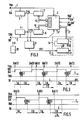
- Figure 1 is a block diagram of a signal phasing device.
- FIG. 2 is the general block diagram of the dynamic switching device according to the invention.
- FIG. 3 is a time diagram making it possible to explain the operation of the dynamic switching device of FIG. 2.
- Figure 4 is the detailed block diagram of a preferred embodiment of the dynamic switching device according to the invention.
- FIG. 5 is a time diagram for explaining the operation of the device of FIG. 2.
- FIG. 1 there are shown two digital channels (or conduits) 1 and 2 which carry at input terminals BA, BB respectively the frame signals TRA and TRB carrying the same information but affected by different delays.
- These are, for example, to fix the ideas of a time-division telephone transmission system at 2048 kbits / s, each frame comprising 32 telephone channels, at the rate of a sample coded on 8 bits for each channel, that is to say frames of 256 bits.
- the maximum phase shift envisaged between the signals TRA and TRB is large and can reach several hundred frames. In the digital example envisaged, this maximum phase shift is for example equal to 256 frames, or 65,536 bits.
- the frame signal comprises, at regular intervals in time, free bits which can be used in particular to convey additional information.
- One of these bits is used to create a low frequency superframe signal whose period T is at least equal to twice the maximum phase shift expressed in bit time (TSI).
- T bit time
- the frequency of the superframe signal is for example equal to 15 Hz.
- Each signal TRA, TRB is supplied on the one hand to a separate frame locking means 3, 4 and to common variable delay means 5 constituted by a double memory.
- the memory 5 is a circular memory of the static dual access RAM type.
- Each frame locking means 3, 4 of conventional design is designed to detect, in the frame signal, the pattern of the low-frequency superframe, to lock onto this pattern and provide a frame synchronization signal SYA, SYB under form of a square signal of period T.
- Each signal SYA, SYB is supplied to a counter 7, 8 and moreover, these two signals are also supplied to a phase comparator 9.
- the phase comparator 9 supplies a pulse signal SYC of period T to a control member 11 which is broken down into a read counter 12 and a coincidence detector 13, the latter receiving the signal SYC and a synchronization signal SYD of period T from the counter 12 and supplying, in the event of phase coincidence of these two signals, a reloading signal SR, on a conductor 14, to the counter 12.
- the counters 7, 8, respectively 12, which are cyclic counters are used for addressing in writing, respectively in reading, of memory 5, by means of address buses 15, 16 for writing, and of a bus 17 for reading.
- a clock generator 18 supplies a clock signal H at the frequency of the data bits (of period TBI) to all the circuits of FIG.
- the clock signal H or, preferably, a derivative signal H 'at the frequency 1 / TBL of the bytes or frames which constitute data blocks is used for writing and reading the data blocks .
- Each write counter 7, 8 is calibrated on the synchronization signal SYA, SYB, its MSB (for example the weight 16) being activated at the frequency 1 / T and its LSB at the frequency of the data bits (signal H ). It is possible, for the write and read addressing, to use all the significant bits of the counters as defined above, in which case the capacity of the memory 5 is equal to the number of data bits contained in a period T of the signal. superframe.
- the MSB is not used for addressing, which makes it possible to reduce the capacity of the memory 5 to half that indicated in the preceding sentence.
- Each location 19 of the memory is double and contains, just before being read, a block of TRA and a block of TRB, these two blocks having the same rank in the period defined by superframe signals which correspond in TRA and TRB , these two blocks therefore carrying the same information apart from transmission errors.
- Reading each memory location provides, on two output terminals BA ', BB', frame signals TRA ', TRB', strictly synchronous.
- the address buses 15 and 16 point to locations for which the rank difference is significant of the time offset ⁇ t to be compensated between frames TRA and TRB.
- the address bus 17 points to a location whose rank is itself offset with respect to the recording of the most late data signal a predetermined number of blocks M x TBL, M being an integer chosen as small as possible according to the application envisaged.
- This operation for controlling the read counter 12 with respect to the write counters 7 and 8, is obtained by means of the phase comparator 9 and the coincidence detector 13.
- the phase comparator performs a double function, the first of which consists in determine which of the two frame synchronization signals SYA and SYB it receives which is the most late.
- the second function is a selection function which can be carried out simply by means of a two-position switch not shown, controlled by the output signal from the state machine.
- the choice terminals of the switch each receive a signal deduced from the signal SYA, respectively SYB, in the form of an impulse signal of the same period (T) by short-term monostable action on the rising edge or, preferably, on the falling edge of the square signal it receives (SYA or SYB).
- the switch then supplies a pulse signal SYC which is the transformed SYA signal or the transformed SYB signal (the most delayed) according to the logic output value of the state machine.
- the coincidence detector 13 receives the signal SYC, and the signal SYD from the read counter 12.
- the signal SYD which is synchronized with the counting cycle of the read counter with a predetermined delay close to the duration MxTBL, has a low duty cycle, very much less than 0.5 and is in the form of an impulse signal of the same period (T) as SYC but whose pulse duration is longer than that of SYC.
- the difference pulse width is adjusted so as to be able to absorb the maximum jitter (of the order of a few tens of bits) which can occur between the clock signal H and the various signals present in the device, in particular between the SYC and SYD signals. If on the other hand the pulses of SYC and SYD do not coincide in time as is the case for example during power-up, a reload signal SR in the form of a logic signal "1" or "0" is transmitted to the reset input (RESET) of counter 12, which has the effect of resetting the pulse of SYD to that of SYC and, simultaneously, restoring the counting of the reading addresses to their nominal value on the understanding that the counter 12 is designed, by construction, to provide the optimal offset between read and write addresses when the signals SYC and SYD are, in substance, in phase.
- the design and arrangement of the circuits 12 and 13, and of the memory 5 for performing the simple functions described above are within the reach of those skilled in the art.
- FIG. 2 shows the input terminals BA and BB carrying the same digital information frame signals TRA and TRB as in FIG. 1.
- the phasing device is symbolized by two variable delay memories 61, 62, controlled from re-phasing control means 63.
- This re-phasing can be carried out by any known means, for example by phase control of the memories 61 and 62, so as to obtain the signals TRA 'and TRB' in phase on the terminals BA 'and BB' which are in this case the choice terminals of a switch 64 whose common terminal CO is the seat of the output signal (SO) of the dynamic switching device according to the invention.
- the phasing device is that described above with reference to FIG. 1.
- Each frame signal is, from its respective input terminal, supplied to a multiple fault detector with several gravity levels 65-1, ..., 65-i, ..., 65-n (respectively 66 -1, ..., 66-i, ..., 66-n).
- Each elementary fault detector receives the signal TRA (respectively TRB) and is designed to detect inside each frame block a given type of error (fault) of given gravity level and to provide a logical error signal, for example "1" in the event of an error in the analyzed block and "0" in the opposite case.
- Severity level 1 is that of a fault corresponding to an error rate and detected by means of a CRC code, the CRC4 code for example; at a higher severity level, level i, an error in a frame alignment word is detected.
- the highest level of gravity, n is that of the signal cutoff, in which case the error signal at the output of the order detector n is maintained throughout the cutoff time.
- the error signals DA (i) (respectively DB (i)) are supplied to a priority encoder 67.
- This priority encoder acts as a partial comparator by comparing the homologous input error signals, from the highest level of gravity to the lowest level of gravity, this comparison being terminated when opposite logical values appear for one of the gravity levels.
- the comparison begins at level n and continues, from a level of gravity i to the level just below i-1 as long as the logic signals, compared two by two, are detected as having the same logic value " 0 "and” 0 "(no error on either of the two blocks at the level considered) or" 1 "and” 1 "(an error on each of the two blocks at the level considered).
- the priority encoder 67 is provided with two outputs 67-A and 67-B connected to the respective inputs R and S of a flip-flop RS 68 whose output Q controls the switch 64.
- the logic values which appear on the outputs 67- A and 67-B are for example inverses of those of the first pair of opposite values detected at input during the comparison which is carried out continuously, sequentially, at the frequency of appearance of the data blocks.
- the appearance of a "1" on the input R (“0" on S) causes the switch or the maintenance (the forcing) of the switch on the terminal BA ', as shown in FIG.
- the truth table of the priority encoder 67 is the following, for two adjacent gravity levels, i and i-1: in the truth table, the sign X designates the logical value "1" or "0" either and Qo designates the previous state of the switch, and implies that the comparison should not be continued at the lower step. It will be noted that this truth table does not account, in dynamic operation, for all the possible logical states of the elements 67, 68 and 64 taken together, while being sufficient however to explain the operation of this subset and allow the skilled in the art.
- the indication BB 'or BA' in the column known as switching only implies a switchover of the switch on this terminal only if the latter was positioned on the other terminal (BA 'or BB') during the block comparison former.
- the indication Q (i-2) implies that the comparison must be continued at step i-2.
- the assembly constituted by the fault detectors with several levels of severity, the priority encoder and the flip-flop RS produces means for masking faults with several levels of gravity.
- the signals TRA, TRB are shown.
- SO and position of switch 64 terminal BA 'or terminal BB'.
- the width of a block is very small and the switching delay with respect to one or other of the TRA and TRB frames less than 2 x TBL can be considered negligible.
- the delay of the least delayed frame signal (delay TA of the signal TRA in this case) which identifies with the fixed delay TF in memories 5, 61 or 62, has been set at a fairly high value of the order of several tens of times the TBL duration to make the figure clearer.
- the delay TA represents the transit time of the signal TRA in the memory 61 (or 5)
- the delay TB is the transit time in the memory 62 (or 5)
- the time ⁇ t representative of the phase shift between TRA and TRB is equal to: TB-TA.
- the state of the counter after incrementation, referenced EDATE at the output of the counter reports each TE date of end of fault.
- the EDATE signal is permanently supplied to the separate date memory 77 via one of the logic gates 78.
- Each fault end date is thus memorized by storing the state of the counter in part j of the separate date memory assigned to the fault DA (j) considered, at each time TE.
- the same counting state (the same date) is stored in the associated date memory (79), in the same memory location as that of the information block coinciding with the end of the fault DA (j) and in the locations following.
- the indication of the fault DA (j) is maintained, on the input j of the priority encoder, that is to say as long as the flip-flop RS 71- j the fault memory is not reset.
- the date associated with this block, SDATE is read simultaneously and supplied, by a conductor 83, to a second input of the comparators 81-1, ..., 81-i, ..., 81-n.
- the comparator 81-j for example, a logic reset signal is supplied, via a gate circuit or 86 at the input of reset (RESET) of the RS 71-j flip-flop in the fault memory.
- RESET reset
- each input of the priority encoder is active since the detection of a fault, for the entire duration of the fault increased by the time of transit of the data in the variable delay memory of the frame signal in question. .
- the operation described below is obtained with reference to FIG. 5 where the same mode of representation is adopted as in FIG. 3.
- an automatic reset of the device is preferably carried out by a watchdog device 87, consisting of a comparator, identical to the comparator 81-i, which receives and compares the EDATE signals and the SDATE signals and supplies, in the event of a tie, via the OR gates 86, a reset control signal common to the flip-flops RS of the fault memory 71-1, ..., 71-i, ..., 71- not. Thanks to the device 87, on power-up, an operating cycle during which the date counter is not incremented, makes it possible to reset the fault memory to zero, which is necessary for initializing the device.
- each cyclic date counter such as 75 to the maximum number of errors likely to occur during the duration TA (respectively TB). This capacity must be large enough so that two identical dates cannot coexist in one or the other associated date memory, which would cause ambiguity during the comparison in 81-1, ..., 81-i, ..., 81-n, since two separate faults cannot be terminated at the same time in the same frame.
- the device according to the invention is produced in the form of integrated circuits.
- an integrated circuit is developed for the production of memory 5 and the two associated date memories and an integrated circuit for the other elements of the device, whether it is the embodiment of FIG. 2 or that of FIG. 4.
Landscapes
- Engineering & Computer Science (AREA)
- Computer Networks & Wireless Communication (AREA)
- Signal Processing (AREA)
- Detection And Prevention Of Errors In Transmission (AREA)
- Radio Transmission System (AREA)
- Time-Division Multiplex Systems (AREA)
Applications Claiming Priority (2)
| Application Number | Priority Date | Filing Date | Title |
|---|---|---|---|
| FR9005412A FR2661578A1 (fr) | 1990-04-27 | 1990-04-27 | Dispositif de commutation dynamique pour le masquage d'erreurs dans un systeme a doublement du conduit numerique. |
| FR9005412 | 1990-04-27 |
Publications (2)
| Publication Number | Publication Date |
|---|---|
| EP0454249A1 true EP0454249A1 (de) | 1991-10-30 |
| EP0454249B1 EP0454249B1 (de) | 1995-01-11 |
Family
ID=9396180
Family Applications (1)
| Application Number | Title | Priority Date | Filing Date |
|---|---|---|---|
| EP91200952A Expired - Lifetime EP0454249B1 (de) | 1990-04-27 | 1991-04-22 | Dynamische Schaltungsanordnung zur Fehlermaskierung in einem System mit Verdoppelung des digitalen Kanals |
Country Status (5)
| Country | Link |
|---|---|
| US (1) | US5237318A (de) |
| EP (1) | EP0454249B1 (de) |
| JP (1) | JPH04229738A (de) |
| DE (1) | DE69106570T2 (de) |
| FR (1) | FR2661578A1 (de) |
Cited By (5)
| Publication number | Priority date | Publication date | Assignee | Title |
|---|---|---|---|---|
| WO1995033322A1 (en) * | 1994-05-27 | 1995-12-07 | British Telecommunications Public Limited Company | Data communication system having channel switching means |
| WO2009022325A2 (en) | 2007-08-13 | 2009-02-19 | Provigent Ltd. | Protected communication link with improved protection indication |
| US7839952B2 (en) | 2006-12-05 | 2010-11-23 | Provigent Ltd | Data rate coordination in protected variable-rate links |
| US8040985B2 (en) | 2007-10-09 | 2011-10-18 | Provigent Ltd | Decoding of forward error correction codes in the presence of phase noise |
| US8315574B2 (en) | 2007-04-13 | 2012-11-20 | Broadcom Corporation | Management of variable-rate communication links |
Families Citing this family (7)
| Publication number | Priority date | Publication date | Assignee | Title |
|---|---|---|---|---|
| GB2267415B (en) * | 1992-05-19 | 1996-02-07 | Sony Broadcast & Communication | Signal switching |
| SE470502B (sv) * | 1992-10-26 | 1994-06-06 | Ericsson Telefon Ab L M | Förfarande och anordning för att minimera en faslägesskillnad mellan två dataströmmar före omkoppling |
| EP0744847B1 (de) * | 1995-05-23 | 2005-08-24 | Koninklijke Philips Electronics N.V. | Redundantes Datenübertragungssystem mit mindestens zwei Kanälen |
| JP2812261B2 (ja) * | 1995-09-13 | 1998-10-22 | 日本電気株式会社 | Atmセルフロー制御装置 |
| US8363744B2 (en) | 2001-06-10 | 2013-01-29 | Aloft Media, Llc | Method and system for robust, secure, and high-efficiency voice and packet transmission over ad-hoc, mesh, and MIMO communication networks |
| GB2474180A (en) * | 2008-07-25 | 2011-04-06 | Smith International | PDC bit having split blades |
| RU2528089C2 (ru) * | 2012-11-15 | 2014-09-10 | Открытое акционерное общество "Головное системное конструкторское бюро Концерна ПВО "Алмаз-Антей" имени академика А.А. Расплетина" (ОАО "ГСКБ "Алмаз-Антей") | Устройство синхронного приема двоичной информации по дублирующим каналам связи |
Citations (3)
| Publication number | Priority date | Publication date | Assignee | Title |
|---|---|---|---|---|
| DE3206749A1 (de) * | 1982-02-25 | 1983-09-08 | Siemens AG, 1000 Berlin und 8000 München | Ersatzschaltung zum umschalten einer, ein digitalsignal fuehrende betriebsstrecke auf einer ersatzstrecke |
| EP0249930A1 (de) * | 1986-06-18 | 1987-12-23 | Alcatel Transmission Par Faisceaux Hertziens A.T.F.H. | Verfahren zur Synchronisation von zwei binären Strömen |
| DE3800977A1 (de) * | 1988-01-15 | 1989-07-27 | Ant Nachrichtentech | Digitalsignal-uebertragungssystem mit linienersatzbetrieb |
Family Cites Families (4)
| Publication number | Priority date | Publication date | Assignee | Title |
|---|---|---|---|---|
| JPS5654141A (en) * | 1979-10-09 | 1981-05-14 | Nec Corp | Band switching circuit without momentary interruption |
| JPS6377235A (ja) * | 1986-09-20 | 1988-04-07 | Fujitsu Ltd | デイジタル通信システムの切替方式 |
| JP2622972B2 (ja) * | 1987-09-17 | 1997-06-25 | 三洋電機株式会社 | Fmラジオ受信機 |
| CA2021232C (en) * | 1989-07-17 | 1993-09-21 | Hiroyasu Muto | Diversity receiving system for use in digital radio communication with means for selecting branch by estimating propagation path property |
-
1990
- 1990-04-27 FR FR9005412A patent/FR2661578A1/fr active Pending
-
1991
- 1991-04-22 EP EP91200952A patent/EP0454249B1/de not_active Expired - Lifetime
- 1991-04-22 DE DE69106570T patent/DE69106570T2/de not_active Expired - Fee Related
- 1991-04-25 JP JP3095114A patent/JPH04229738A/ja active Pending
- 1991-04-29 US US07/693,975 patent/US5237318A/en not_active Expired - Fee Related
Patent Citations (3)
| Publication number | Priority date | Publication date | Assignee | Title |
|---|---|---|---|---|
| DE3206749A1 (de) * | 1982-02-25 | 1983-09-08 | Siemens AG, 1000 Berlin und 8000 München | Ersatzschaltung zum umschalten einer, ein digitalsignal fuehrende betriebsstrecke auf einer ersatzstrecke |
| EP0249930A1 (de) * | 1986-06-18 | 1987-12-23 | Alcatel Transmission Par Faisceaux Hertziens A.T.F.H. | Verfahren zur Synchronisation von zwei binären Strömen |
| DE3800977A1 (de) * | 1988-01-15 | 1989-07-27 | Ant Nachrichtentech | Digitalsignal-uebertragungssystem mit linienersatzbetrieb |
Cited By (7)
| Publication number | Priority date | Publication date | Assignee | Title |
|---|---|---|---|---|
| WO1995033322A1 (en) * | 1994-05-27 | 1995-12-07 | British Telecommunications Public Limited Company | Data communication system having channel switching means |
| US7839952B2 (en) | 2006-12-05 | 2010-11-23 | Provigent Ltd | Data rate coordination in protected variable-rate links |
| US8315574B2 (en) | 2007-04-13 | 2012-11-20 | Broadcom Corporation | Management of variable-rate communication links |
| WO2009022325A2 (en) | 2007-08-13 | 2009-02-19 | Provigent Ltd. | Protected communication link with improved protection indication |
| EP2176956A4 (de) * | 2007-08-13 | 2010-09-29 | Provigent Ltd | Geschützte kommunikationsverbindung mit verbesserter schutzindikation |
| US8001445B2 (en) | 2007-08-13 | 2011-08-16 | Provigent Ltd. | Protected communication link with improved protection indication |
| US8040985B2 (en) | 2007-10-09 | 2011-10-18 | Provigent Ltd | Decoding of forward error correction codes in the presence of phase noise |
Also Published As
| Publication number | Publication date |
|---|---|
| JPH04229738A (ja) | 1992-08-19 |
| US5237318A (en) | 1993-08-17 |
| DE69106570T2 (de) | 1995-08-24 |
| FR2661578A1 (fr) | 1991-10-31 |
| EP0454249B1 (de) | 1995-01-11 |
| DE69106570D1 (de) | 1995-02-23 |
Similar Documents
| Publication | Publication Date | Title |
|---|---|---|
| EP0454249B1 (de) | Dynamische Schaltungsanordnung zur Fehlermaskierung in einem System mit Verdoppelung des digitalen Kanals | |
| EP0113307B1 (de) | Anpassungseinrichtung für digitale Informationsblöcke fester Länge | |
| EP0041429B1 (de) | Verfahren und Einrichtung zur Synchronisierung digitaler Signale | |
| FR2508742A1 (fr) | Circuit pour synchroniser le fonctionnement d'un emetteur et d'un ou plusieurs recepteurs radioelectriques | |
| EP0136757B1 (de) | Sendeempfangsstelle für ein Informationsübertragungssystem nach dem Frequenzsprungverfahren | |
| EP0487428A1 (de) | Anordnung für synchrone Informationsübertragung über ein asynchrones Netzwerk, insbesondere über ein ATM-Netzwerk | |
| FR2466916A1 (fr) | Controleur de terminal d'un systeme de transmission a acces multiples par repartition de temps microprogrammable | |
| FR2466837A1 (fr) | Memoire tampon d'interface terrestre a acces multiples par repartition de temps pour operations entrelacees | |
| FR2466921A1 (fr) | Appareil d'affectation et de selection de parties de canaux de transmission de donnees | |
| EP0680170B1 (de) | Übertragungsanordnung für ein Leitungskodiertes Signal über eine Fernsprechleitung mit Frequenzsynchronisierungsschaltung | |
| EP0454246B1 (de) | Phasenkorrekturschaltung für Signale in einem System mit doppelten digitalen Leitungen | |
| FR2647612A1 (fr) | Dispositif, procede et reseau de transmission de donnees multipoint et multicanal | |
| CH640678A5 (fr) | Procede et installation de transmission simultanee d'une onde basse frequence et d'un signal numerique mic. | |
| EP0137563B1 (de) | Umschaltungsverfahren mit automatischem Phasenausgleich der Daten über +/- 3,5 Bits und Vorrichtung zur Durchfürung des Verfahrens | |
| EP0097579A1 (de) | Funkverbindungssystem nach dem Frequenzsprungverfahren mit Redundanz zwischen den einzelnen Frequenzstufen | |
| EP0064923B1 (de) | System zur Phasensynchronisation digitaler Datenströme und seine Verwendung bei der Umschaltung der Datenströme | |
| EP2428011A1 (de) | Demodulator und system zum übertragen von modulierten informationen insbesondere für hochfrequenzidentifikationsetiketten | |
| FR2728422A1 (fr) | Systeme de radio-communication permettant de gerer des retards de transmission variables | |
| EP0037770B1 (de) | System zur paketweisen Übertragung digitaler Daten unter Verwendung eines besonderen Typs von Synchronisationsworten | |
| EP1049281A1 (de) | TDMA-Mehrpunkt-zu-Punkt-System unter Verwendung einer besonderen Burststruktur und dazugehöriger Sender | |
| EP0717575A2 (de) | Funk-Kommunikationssystem mit verteilten Feststationen | |
| EP0018618B1 (de) | Vorrichtung zur Synchronisierung eines Multiplexers in einer Zeitmultiplex-Vermittlungsstelle | |
| EP0688115B1 (de) | Übertragungssystem mit mindestens zwei Übertragungskanälen zwischen einem Sender und einem Empfänger, sowie Empfänger für ein solches System | |
| CA2132626C (fr) | Installation de transmission de donnees, du type reseau radio, et procede correspondant | |
| EP0216720B1 (de) | System zur bitseriellen Zusammensetzung von Paketmultiplexsignalen |
Legal Events
| Date | Code | Title | Description |
|---|---|---|---|
| PUAI | Public reference made under article 153(3) epc to a published international application that has entered the european phase |
Free format text: ORIGINAL CODE: 0009012 |
|
| AK | Designated contracting states |
Kind code of ref document: A1 Designated state(s): DE FR GB |
|
| RAP1 | Party data changed (applicant data changed or rights of an application transferred) |
Owner name: N.V. PHILIPS' GLOEILAMPENFABRIEKEN Owner name: TRT TELECOMMUNICATIONS RADIOELECTRIQUES ET TELEPHO |
|
| K1C1 | Correction of patent application (title page) published |
Effective date: 19911030 |
|
| 17P | Request for examination filed |
Effective date: 19920429 |
|
| 17Q | First examination report despatched |
Effective date: 19940321 |
|
| GRAA | (expected) grant |
Free format text: ORIGINAL CODE: 0009210 |
|
| AK | Designated contracting states |
Kind code of ref document: B1 Designated state(s): DE FR GB |
|
| REF | Corresponds to: |
Ref document number: 69106570 Country of ref document: DE Date of ref document: 19950223 |
|
| GBT | Gb: translation of ep patent filed (gb section 77(6)(a)/1977) |
Effective date: 19950406 |
|
| PLBE | No opposition filed within time limit |
Free format text: ORIGINAL CODE: 0009261 |
|
| STAA | Information on the status of an ep patent application or granted ep patent |
Free format text: STATUS: NO OPPOSITION FILED WITHIN TIME LIMIT |
|
| 26N | No opposition filed | ||
| REG | Reference to a national code |
Ref country code: FR Ref legal event code: TP |
|
| REG | Reference to a national code |
Ref country code: FR Ref legal event code: TP |
|
| REG | Reference to a national code |
Ref country code: FR Ref legal event code: CD |
|
| PGFP | Annual fee paid to national office [announced via postgrant information from national office to epo] |
Ref country code: GB Payment date: 19990420 Year of fee payment: 9 |
|
| PGFP | Annual fee paid to national office [announced via postgrant information from national office to epo] |
Ref country code: FR Payment date: 19990427 Year of fee payment: 9 |
|
| PGFP | Annual fee paid to national office [announced via postgrant information from national office to epo] |
Ref country code: DE Payment date: 19990624 Year of fee payment: 9 |
|
| PG25 | Lapsed in a contracting state [announced via postgrant information from national office to epo] |
Ref country code: GB Free format text: LAPSE BECAUSE OF NON-PAYMENT OF DUE FEES Effective date: 20000422 |
|
| GBPC | Gb: european patent ceased through non-payment of renewal fee |
Effective date: 20000422 |
|
| PG25 | Lapsed in a contracting state [announced via postgrant information from national office to epo] |
Ref country code: FR Free format text: LAPSE BECAUSE OF NON-PAYMENT OF DUE FEES Effective date: 20001229 |
|
| PG25 | Lapsed in a contracting state [announced via postgrant information from national office to epo] |
Ref country code: DE Free format text: LAPSE BECAUSE OF NON-PAYMENT OF DUE FEES Effective date: 20010201 |
|
| REG | Reference to a national code |
Ref country code: FR Ref legal event code: ST |